Note: Descriptions are shown in the official language in which they were submitted.
WO 93/24905 ~ ~ ~ ~ ~ ~ ~ PCT/US93/05277
SYSTEM CONTROLLER AND REMOTE FAULT A,NNUNCIATOR
WITH COOPERATIVE STORAGE, SHARING, AND
PRESENTATION OF FAULT DATA
BACKGROUND OF THE INVENTION
Many types of control systems are used to operate apparatus which has
the potential for causing harm or injury if various parameter levels are
outside of
predetermined ranges. A simple example is the automobile whose engine will be
severely damaged if the oil pressure is too low or the coolant temperature is
too high.
, In this situation the system relies on the good judgment of the driver to
stop the auto
as soon as the warning light or gauge indicates the problem. In some systems
too, it
is desirable to simply monitor operation of various aspects of a system.
In many of these systems however, human monitoring of the apparatus
parameters may be unacceptable because the apparatus is intended to operate
i 5 automatically, or because the result of improper, that is to say human,
monitoring
may result in serious damage or injury. Neither is it desirable to rely on the
control
system to monitor every one of these parameter levels and shut down the system
when
needed because this adds substantial complexity to the controller. Also, the
control
system can on occasion fail, for example because of power outages. Instead, in
most
2 o systems these parameters are used to directly control interlock switches
which open if
th,°, parameter level is outside of the predetermi~d range. In these
systems, the
interlock switches are .typically arranged in a series circuit which passes
the current
for operating the apparatus (and parts of the control system as well in many
cases) so
that if any of the parameter levels are outside the range specified for it,
the apparatus
25 will not receive power and cannot operate. Examples of these series
circuits of
interlock switches are found in a number of different types of apparatus and
their
controls, including as one example burner systems and controls. In burner
controls,
the interlock switch series circuit is used to control power which operates
the fuel
valves. If any of the burner system parameters are outside the specified
ranges,
3 0 power is not available to the fuel valves, with the result that the burner
cannot
operate.
One problem which arises in these systems is determining the cause of
a malfunction. If an interlock switch opens, power to the system is
interrupted of
course, but the problem can be in any of the parameters controlling the
interlock
3 5 switches or in other ,aspects of the system. For example, in burner
systems flame
failure does not control an interlock switch. In this particular situation,
the control
system itself interprets the flame sensor signal and shuts down the fuel
valves when
flame is detected as absent. When the shutdown is caused by an open interlock
WO 93/24905 PGT/US93/05277
2
~1~9 ~. ~2
switch, by the time a repairer arrives to correct the problem, the original
cause of the
shutdown may no longer exist. As one example of this situation, a low fuel
pressure
parameter which opens an interlock switch may have been restored within a few
seconds and thus will not be apparent to the repairer. Even when latching
interlock
switches are used, on occasion a second fault may occur after the first fault
and before
the diagnostic procedures can be started. It is then difficult to determine
the cause of
the original shutdown. Early annunciators for use with these switch strings
simply
showed current status of the switches, which was not always adequate for easy
troubleshooting.
1 o In order to simplify and improve troubleshooting of malfunctions in
these systems, improved annunciators have been designed which record the
status of
each of the interlock switches in the interlock switch string at the time a
fault is
detected: Thus for example, U.S. Patent No. 4,295,129 (Cade) describes a
circuit
connected to individual interlock switches and the main and pilot valve
actuators, to
detect abnormal conditions by sensing the status of the fuel valves and to
record the
identity of the first interlock switch or fuel valve to open at the time the
abnormal
condition was detected. U.S. Patent No. 3,967,281 (Dageford) attempts to
determine
the earlier of two detected failures and record the identity of the switch
which first
opened. These will typically be related, but may happen in either order, and
an
2 0 indication of the earlier allows easier detection of the underlying
problem.
Frequently, knowledge of the current status is helpful during
troubleshooting. A problem with the present systems is that it is not possible
during
troubleshooting, without losing the first out status, to determine the current
status of
the switches without individually testing or inspecting them. While such
individual
testing or inspecting is possible, it is laborious when a large number of
switches are
involved. Furthermore, the current states of these switches may change during
the
troubleshooting, resulting in further troubleshooting problems.
It frequently is undesirable to build a high level first out fault detection
directly into the controller for the system. There may be system configuration
3 0 advantages in separating the switch status annunciator functions from the
control
functions. For example, the interlock switches may be physically located at
some
distance from the controlled system. Or the control system may have a
deliberate
modular design to accommodate users who may not need a high level of fault
detection. hi such systems, it is frequently convenient to use a simple serial
3 5 communication path between the annunciator and the controller. Such a
communication path is easy to install, and the transceivers which implement
its use
are cheap and allow reliable communication. Frequently, such a path will be
shared
WO 93/24905 ~ ~ ~ (~ ~ ~ ~3_ PGT/US93/05277
by a number of modules, say other controllers, if a number of independent
systems
are involved, or a display module which may have yet a third physical
location.
In such a system, fault detection, as opposed to switch status
information, is still typically included in the controller, since this
dramatically
improves the reliability and speed of the controller in responding to fault
conditions as
they occur. However, the use of a shared serial communication path means that
the
annunciator for a particular interlock switch series circuit may not receive
notification
of a fault until some time after the fault has actually occurred. Since this
time
between fault detection and notification to the annunciator may be appreciable
in
certain instances, say on the order of hundreds of milliseconds, switch status
may
have changed and the first out information then provided by the annunciator
will be
incorrect. Inaccurate first out information has the potential to dramatically
worsen the
problem of fault diagnosis. Accordingly, there is a motivation to improve the
accuracy of first out information provided in the situation described.
There are also situations where switch status may be desired even
though a fault has not occurred. For example, during startup or shutdown of an
installation, switches in a series circuit may be scheduled to close or open
at particular
stages, and certain installatioas may find it useful to log this information
even though
no fault has been sensed.
BRIEF DESCRIPTION OF THE INVENTION
In order to comprehensively determine the status of a series switch
circuit, I have determined that it is necessary to keep a history identifying
the status of
a switch, which most frequently will be the first out switch, at each instant
of recently
2 5 elapsed time. I use a status recorder for recording the status history of
at least one of
a plurality of interlock switches each having a pair of contacts, where said
contacts
are connected by a plurality of conductors to form a series circuit of
interlock
switches iwa preselected sequence. The series circuit is connected to pass
current
from a power source to a load. The status recorder includes a plurality of
voltage
3 0 sensors each associated with an interlock switch. Each voltage sensor is
coimected to
a conductor connected to the interlock switch with which the voltage sensor is
associated and provides a status signal having a first state responsive to
presence of
power voltage on the conductor to which it is connected and a second state
otherwise.
The status recorder further comprises
3 5 a) signal selector means receiving the status signals for providing a
selector signal encoding the status of at least one selected interlock switch;
.
b) a status register receiving the selector signal and a status change
signal, recording the information encoded in the selector signal responsive to
the
WO 93/24905 Q~'~ ~~ ' PGT/US93/05277,..
-4-
status change signal, and providing a status register signal encoding the
contents of
the status register;
c) an oscillator issuing a clock signal having level changes at preset
intervals;
d) a counter receiving the clock signal, changing an internally stored
time stamp value by a fixed amount responsive to each level change in the
clock
signal, and providing a time stamp signal encoding the time stamp value;
e) status change sensing means receiving the selector signal from the
signal converter and the status register signal for comparing the information
encoded
1 o in the selector signal and the status register signal, and responsive to
disagreement
therebetween, providing the status change signal; and
f) a memory receiving the status change signal, the status register
signal, and the time stamp signal, for sequentially recording responsive to
each status
change signal, a history entry comprising the information encoded in the
status
register signal and the time stamp value encoded in the time stamp signal, and
for
providing a history signal encoding recorded history entries.
The information most often of interest and also most easily determined
is the identity of the first out switch. The status recorder described above
may be
modified to record first out information by assigning to each of said
interlock switches
2 o a unique identification number. Further, each voltage sensor has assigned
to it the
identification number of its associated interlock switch. The signal selector
means
comprises a signal converter receiving the status signals from the voltage
sensors.
The signal converter provides as the selector signal a first out signal
encoding the
identification number of an irnerlock switch with which is associated a
voltage sensor
2 5 currently providing a status signal having the second state and connected
to the
contact of a switch also having a contact connected through a conductor to a
voltage
sensor providing a status signal having the first state. The status register
comprises a
first out register recording the identification number encoded in the status
signal. The
memory comprises means recording the identification number encoded in the
first out
3 0 register signal. Of course, the time stamp value is recorded with each of
the history
entries encoding the first out identification number.
A system which can interpret and use the switch status information of
the history signal and which includes the modified status recorder described
in the
paragraph above has in the status recorder a memory including a plurality of
storage
35 locations, each storage location recording a single history entry. The
system further
comprises a controller including l) request means for providing a request
signal
responsive to a preselected controller condition and ii j a request timer
holding a
frequently updated request time value specifying the time currently elapsed
since the
WO 93/24905 ~ ~ ~ ~ ~ PCT/US93/05277
-5-
request signal was provided and providing a request ~~me signal encoding the
current
request time value. Because of the data transmissic protocols involved as
explained
earlier, the status recorder in such a system may well not receive a request
signal for
some time after the request has actually occurred.
In this system, the status recorder cooperates with an analyzer
comprising
a) a delay timer receiving the request time signal and updating a delay
time value at the rate of the request timer, and providing a transmit delay
time signal
encoding a transmit delay time value equalling at least the sum of the delay
time value
and the request time value; and
b) entry selection means receiving the transmit delay time signal and
the history entries encoded in the history signal, for selecting on the basis
of a
comparison of the time stamp values in the history entries with the transmit
time delay
value, at least one history entry recorded in the memory and for providing the
identification number recorded therein as a first out signal responsive to
said provided
identification number equalling one of a preselected set of identification
number
values.
BRIEF DESCRIPTION OF THE DRAWINGS
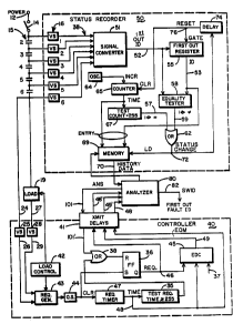
2 o Fig. 1 is a block and logic diagram of the status recorder and a
controller which requests the status information recorded by the status
recorder.
Fig. 2 shows the arrangement of the data in the memory of the status
recorder.
Fig. 3 is a block and logic diagram of the analyzer block of Fig. 1
which determines the first out switch status at the time of a request signal.
Fig. 4 is a flow chart of software code which may be executed by a
suitable microprocessor to implement an alternate process for recording status
information in a memory of the microprocessor.
3 0 DESCRIPTION OF THE PREFERRED EMBODIMENT
Turning first to Fig. 1, a system which is to be controlled is shown as
comprising a load 19 which receives its .operating power from a power source
12
through series circuit comprising a master switch 14 and other interlock
switches
shown generally at 15. Each interlock switch includes a pair of contacts by
which
3 5 individual conductors connect the switches to form the series circuit. The
interlock
switches 15 are given unique identification numbers by which they are
specified, and
exemplary identification numbers have been written just to the left of each of
them.
WO 93/24905 0~', ~ PCT/US93/05277
,.,.,>,
-6-
While only six switches are shown in this embodiment, many systems may use a
dozen or more.
The conduction status of each of the interlock switches is generally
controlled by a physical parameter which must fall within a certain range for
safe
operation of the load either before or during the load startup operations. For
example, if the load is a burner, certain of the interlock switches will be
controlled by
parameters associated with the burner's fuel supply. If the parameter is fuel
pressure
which becomes too low or high at any time then one of the switches in the
series
circuit 15 will open. If a combustion air fan fails to operate during startup,
then an
1 o air flow sensor causes an interlock switch in series circuit 15 to remain
open. In the
burner example, the load may comprise the fuel valves and ignition needed for
proper
operation. It can be seen that the function of series circuit 15 and the
parameters
associated with their operation serve to prevent operation of the load if not
safe to do
so.
One can see that the interlock switch closest in the series circuit 15 to
the power terminal and which is open, will have power voltage on one of its
contacts
only, and that all of the conductors between that contact and the power
terminal will
also carry power voltage. Conversely, none of the other conductors will carry
power
voltage. It is conventional to refer to the open interlock switch which is the
open
2 o switch closest to the power terminal 12 as the first open or first out
switch.
Voltage sensors 16 receive on their input terminals the voltage present
at the connectors between adjacent pairs of contacts of interlock switches in
the series
circuit 15. Each of the voltage sensors 16 provides on one of the output paths
38 a
status signal having first and second states accordingly as voltage is absent
or present
on the connector to which its input terminal is connected. The status signals
will
reveal the fast out switch, by each having second states where the voltage
sensors are
connected to conductors between the first out switch and the power terminal,
and first
states otherwise. The individual voltage sensors 16 are also identified by
individual
identification numbers place adjacent to each and related to the interlock
switches'
3 o identification numbers, such that each voltage sensor is connected to the
conductor
attached to the downstream (from the power terminal 12) contact of the switch
having
that identification number.
Other than voltage sensors 16, all of the individual elements shown in
status recorder 50 will usually comprise a suitable programmed microprocessor.
(By
3 5 "microprocessor" is meant any of the small computing devices incorporated
in one or
more microcircuits which are intended for mounting on a circuit board and have
an
addressable random access data storage memory (RAM).) The reader who is
skilled
in the art will realize that a part of a microprocessor which executes the
functions of
WO 93/24905 ~ ~ ~ ~ ~ ~ ~ PCl'/US93/05277
the various elements shown as comprising status recorder 50 in fact comprises
each of
these elements as its function is performed. The functional relationship and
descriptions shown in Fig. 1 for the elements of status recorder 50 provides
ample
guidance for a person who is skilled in the art to replicate the invention in
a
microprocessor should (s)he choose this implementation. Each of the blocks
shown
for status recorder 50 have well known functions, and hardware products are
available
as well or can be easily devised from available hardware elements for
performing
these functions. The blocks shown as forming a part of controller 40 will
typically
also comprise a microprocessor. The elements of controller 40 which interact
directly
with analyzer 80 are also well known. The structure and operation of analyzer
80 is
explained and discussed in connection with Fig. 3. Lastly, the symbol " _ > "
used at
various points throughout Figs. 1 and 3 has the conventional meaning of
"implies" or
"results from" . Thus, in connection with count test element 67, the legend "
1 = >
_ " means that path 58 carries a logical 1 signal when the count accumulated
in
counter 65 equals 255.
A signal converter 51 receives the status signals on paths 38 from the
voltage sensors, and provides on path 52 a first out signal encoding the
identification
rnimber for the current first open switch if there is one. Other formats for
encoding
the identity of the first out interlock switch are also possible. When load 19
is in its
2 0 normal operating mode, all of the switches comprising the series circuit
15 are closed,
meaning that there is no first open switch. In this situation for the example
shown,
the signal converter 51 provides a first out signal encoding an identification
number of
seven as an "all closed" value, although any value different from every switch
identification number may be used. The structural details of the signal
converter 51
are not important, and there are a number of well-known ways by which this
element
may be implemented.
The first out signal is provided as an input to a first out register 55.
The identification number encoded in the first out signal is recorded in the
first out
register 55 when a RESET signal on path 76 is applied to the gate of register
55.
3 0 Register 55 provides the identification number recorded in it in a first
out register
signal on path 53. An equality tester 58 receives the identification numbers
encoded
in the first out register signal on path 53 and the first out signal on path
52. If the
identification numbers received by equality tester 58 on paths 52 and 53 are
equal as
they usually are, then a signal provided on path 59 to an OR gate 62 by
equality tester
58 has a logical 0 value. If the identification numbers received by tester 58
from
signal converter 51 and register 55 are unequal, then tester 58 provides a
logical 1
signal as the signal on path 59 to OR gate 62.
WO 93/24905 PCT/US93/05277
a,,,,
~~.~'~ ~ _8_ ..
A second input to OR gate 62 is provided by a count tester 67. At all
times while history of the switches' status is being recorded, an elapsed time
value
(TIME) during which the first out register 55 contents remain unchanged, is
accumulated in a counter 65. Counter 65 contains a value which is incremented
in
response to level changes occurring at fixed intervals in a clock signal from
oscillator
64. In my preferred embodiment, the interval between these changes is 8 ms.,
which
I have found to provide sufficient accuracy without an excessive number of
bits to
record these time values, but other interval lengths are suitable also.
Counter 65 is
cleared by a logical 1 signal on its clear (CLR) terminal when the RESET
signal on
1 o path 76 has a logical 1 value. The contents of counter 65 is supplied to
the input of a
test element 67 which tests the value stored by counter 65 to be equal to 255.
This
value is also arbitrary, and is chosen simply because it is the maximum value
which
can be stored by eight bits. If the contents of counter 65 are equal to 255,
then a
logical 1 signal is applied to a second input of OR gate 62.
The output of OR gate 62 is a status change signal, which has a number
of purposes within this apparatus. The status change signal is applied to a
load (LD)
terminal to condition a memory 69 to accept a history entry comprising the
contents
of the first out register 55 and the counter 65. Fig. 2 shows the organization
of
memory 69. In my embodiment, there are locations in memory 69 for 16 history
2 o entries, each location having fields for recording an identification
number (ID NO)
field and a time stamp (TIME) field. Each memory location has its own
sequential
index assigned to it. Memory 69 is addressed such that individual entries are
loaded
into sequentially indexed locations, with circular or closed indexing where
index 0
location following the index 15 location. The initial value of the index is
not
important because of this circular sequencing of location indices while
loading history
entries into memory 69. Each successive status change signal causes memory 69
to
store the current contents of counter 65 and first out register 55 in the
location
immediately following the location where the previous history entry was
stored.
Individual history entries are provided responsive to a read (RD) signal, by
memory
3 0 69 on path 70 in a history signal encoding the values of the first out
register contents
and counter contents which form the history entries. Individual entries may be
retrieved by a read signal encoding the index values of these entries. Those
with
familiarity with the art realize that this organization of memory 69 is
completely
conventional.
3 5 The status change signal is also applied to the input of a delay element
74 which provides the reset signal on path 76 a short time after the status
change
signal appears. The delay in delay element 74 need only be long enough to
allow the
history entry to be recorded by memory 69 before the reset signal causes the
contents
WO 93/24905 ~ ~ ~ ~ ~ ~ ~ . PCT/US93/05277
-9-
of first out register 55 to possibly change by gating in a new first out
identification
number, and the contents of counter 65 to change by being cleared from some
typically non-zero value (zero is possible but unlikely) to zero. The first
out register
contents will not change of course if the status change signal arose from the
counter
65 contents reaching 255.
The effect of the two conditions which produce logical 1 inputs to OR
gate 62 is to cause memory 69 to record, with 8 cosec. accuracy, the length of
time a
particular switch status persists before changing. If the switch status exists
unchanged
for 256 x 8 cosec. = approximately 2 sec. or more from the time of the
previous reset
1 o signal, then a history entry having 255 in the TIME field and its ID NO
field equal to
the number on path 53 results. This is in fact a common situation. During
normal
run mode of the load 19, each of the interlock switches will be closed; with
the result
that the first out signal on path 52 has the all closed value of 7 for an
extended
interval. Memory 69 will fill up with' history entries each of the form 7 255
for the
ID NO and TIME fields respectively. Even during a typical startup phase of
operation, it is expected that at some point well before run mode is entered
all of the
interhck switches will have closed. It can be seen that with this
configuration for
memory 69, after approximately 32 sec. of stability in the interlock switch
status, all
of the memory locations will contain 7 255.
2 o The history entries are supplied to an analyzer 80 on path 70 for use in
determining the likely source for a fault detected in the operation of load
I9. The
analyzer 80 and the status recorder 50 together with a display unit comprise
an
expanded annunciator system which cooperates with a controller 40 in assisting
the
operator of the installation comprising load 19 in diagnosing operating
faults.
Many of the components shown as comprising controller 40 are
typically also implemented by programming a suitable microprocessor.
Controller 40
includes a load control element 42 which provides control signals to load 19
which
control its operation. Voltage applied to load 19 through interlock switches
15 from
power terminal is sensed by a voltage sensor 25 which provides a logic level
interlock
3 0 signal on path 26 having first and second values as load power is and is
not present on
path 24. Presence of voltage at a selected point within load 19 may also be
supplied
to fault sensor 43 as a logic level signal by voltage sensor 28. The signals
on paths
26 and 29 are collectively referred to as load status signals.
A request generator element 43 receives the control signals from load
control element 42 and the load status signals. If at any time the load status
signals
do not agree with the values expected for the current configuration of the
control
signals, this is interpreted by the request generator 43 as a fault condition,
and a
request signal is provided to a one-shot 44 which in response provides a short
signal
WO 93/24905 ~ ~~~ PGTJUS93/05277
~,'~.~' -10-
to the set (S) terminal of a flip-flop 36 as well as to the clear (CLR) input
of a request
timer 47. A request signal starts the process by which a first out switch as
of the time
of the request signal is identified. Request signals may be provided for
reasons other
than faulty operation of the load 19, according to some preselected condition
which
occurs within request generator 43, but which arises for example because of
operator
input to controller 40. When set, flip-flop 36 provides on its Q output
terminal a
request (REQ) signal carried on path 46 to a transmit delay block 41 and a
error
detection code (EDC) element 45. The request timer 47 has an internal request
time
value which is incremented at preselected intervals and encoded in a request
time
1 o signal which specifies the time elapsed since the request condition was
detected by
request generator 43.
Controller 40 does not make any determination as to the status of the
switches at the time of the 'request. Instead the request and the request time
signals
are sent to analyzer 80 via a communication bus and are used by it to select
information in memory 69 which records the switch status at the time of the
request.
In my commercial embodiment this data transmission occurs via a serial data
path
shared with at least one display unit, and possibly with a number of other
devices as
well. The use of a shared serial data path simplifies installation, and the
receiver/transmitters for performing these transmissions are widely available,
reliable,
and cheap. Use of a shared serial data bus however, creates essentially random
delays
in the communication of data between analyzer 80 and controller 40. These
delays
arise most frequently because of conflicts in the use of the data path. To
simplify the
explanation of the embodiment, I have shown the data link between controller
40 and
analyzer 80 as comprising parallel data paths for each type of data
transmitted, with a
transmission delay block 41 interposed therein to represent these delays. The
request
signal carried on data path 46 is represented in Fig. 1 as available, delayed
in time, to
analyzer 80 on data path 46' . The request time signal carried on path 48 is
provided
to analyzer 80 on data path 48' under similar conditions.
To assure accuracy of the data provided to analyzer 80, it is customary
to append an error detection code to the end of each message. A simple sum
check is
usually adequate for the non-critical information involved here. The EDC
element 45
receives the request and request time signals, as well as any other data
included in the
message to analyzer 80 and shown as the input on path 37, and forms an error
detection code from all of the bytes which form preceding parts of the
message. EDC
3 5 element 45 provides a error detection code signal on path 49 which is also
transmitted
through the transmit delay block on the serial path and is carried on path 49'
to
analyzer 80. The EDC signal is used as an end of message (EOM) signal by
analyzer
80.
pfT/US93/05277
WO 93/24905
-11-
The contents of request timer 47 are supplied also to a test element 35
which provides a logical 1 output to one input of an OR gate 38 when the
request time
exceeds some preselected value shown as 255 in Fig. 1. The time uses by test
element 35 puts a maximum limit on the time during which the message can be
sent to
analyzer 80 and the first out switch identification completed. The OR gate 38
also
receives an answer (ANS) signal on path 101' from analyzer 80. When a logical
1 is
present at either input of OR gate 38, a logical 1 output is provided which
resets flip-
flop 36 and changes the request signal from a logical 1 to a logical 0.
Structure and operation of analyzer 80 are defined in Fig. 3. Because
to of the variability of the delays in transmitting the request and request
time signals to
analyzer 80, it is necessary to use the value encoded in the request time
signal in
selecting the proper history entry in memory 69. But there is also an
appreciable
delay while the message itself is sent, and there are synchronization and
other internal
delays within analyzer 80 itself for which account must be made in the history
entry
selection process to accurately determine the switch status at the time the
request
condition was detected.
At the instant that the last of the request time signal is received by
analyzer 80, the request time is provided on path 48' to one input of a delay
timer
register 95, and gated into register 95 by a logical 1 signal on path 88. The
end of
2 o the request time portion of the message on path 48' is sensed by a byte
counter 92
which simply counts each byte in the message and when the byte containing the
last of
the request time is received, places a logical 1 signal on the output
connected to the
input of an AND gate 85 as indicated by the legend on the output of byte
counter 92.
Of course, there are other ways which may be used to determine the end of the
request time signal. The request signal on path 46' forms a second input to.
AND gate
85. The output of AND gate 85 is provided to the set (S) input of a timer flip-
flop 89
and to the load (LD) gate of delay timer register 95. When set, flip-flop 89
provides
an enable signal to an AND gate 90 which starts register 95 incrementing at
the rate
of oscillator 64. The output of AND gate 85 applied to the LD terminal of
register 95
3 0 preloads- register 95 with the request time value carried on path 48' .
The current
contents of register 95 thus closely track the total time elapsed since the
request
generator 43 provided the current request signal.
I use the successful completion of an error detection test as an end of
message signal whose occurrence enables selection of a history entry. An error
test
3 5 element 81 receives the entire message sent to analyzer 80, recalculates
the EDC, and
tests the recalculated EDC against the EDC received at the message end. If the
two
EDC values agree, then a logical 1 signal is placed on path 84. The logical 1
signal
on path 84 is applied to the reset (R) terminal of flip-flop 89, whose "Q"
output
WO 93/24905 ~~~~ PCT/US93105277
e.,s~,
_12_
.. .
changes from a logical 1 to a logical 0 in response. The logical 0 from flip-
flop 89
disables AND gate 90, which stops time accumulation in register 95. At this
point,
register 95 contains a time 1 value which is quite close to the actual time
which has
elapsed since the request signal was first provided by one-shot 44.
The output of error test element 81 is also provided to one input of an
AND gate 83. The second input of AND gate 85 is provided by the request signal
on
path 46'. When both of these inputs have a logical 1, then the AND gate 83
inputs
are satisfied, and a logical 1 signal is generated on path 91. This logical 1
signal on
path 91 forms an enable signal which activates further processing which
identifies the
first out switch.
The delays arising from the transmission of the data to analyzer 80 are
provided from register 95 on path 96 to an adder 86. There are certain other
delays
associated with the operation of the analyzer itself, and an approximation
these are
provided to another input of adder 86'cn path 87. I say "approximation"'
because of
the fact that these delays are somewhat unpredictably variable, arising from
synchronization and other types of delays which arise. As an example of one
such
delay, because oscillator 64 is not synchronized with the incrementation of
the
contents of request timer 47 within controller 40, there is the possibility
that there
may be as much as -8 cosec. to +8 cosec. error in the value in register 95
arising from
2 0 this source itself. There will typically be other sources and sizes for
errors in such an
arrangement, and these will vary from design to design and from occurrence of
one
request to another. I have found that the maximum sum of such uncertainty in
the
delays in my design is not large enough to impact the validity of the
selection of the
history entry from memory 69 and believe that this will be true for most
designs. I
2 5 prefer to perform a worst case analysis of these analyzer delays, and use
the,
maximum possible value for the analyzer delay value provided on path 87. The
enable signal on path 91 causes adder 86 to sum the transmission delays and
the
approximation of the analyzer delays to form an approximation of the total
delays
between the instant of the request signal and the actual determination of the
first out
3 0 switch. The adder 86 provides a signal on path 102 encoding this
approximation.
The time required for the operations performed by analyzer 80 after-this point
are
included in the analyzer delays signal on path 87, allowing the value on path
102 to
be used to determine the approximate time of the request without further
update.
A two step process is used to determine the first out status of interlock
3 5 switches 14 and 15 as of the time the request is detected . In the first
step, a running
total element 97 receives the TIME entries encoded in the history entries from
the
memory 69 on path 70. Element 97 when enabled by the signal on path 91
sequentially extracts TIME values starting from the most recently stored of
the history
21 ~ 91 ~ Z p~/US93/05277
WO 93/24905
-13-
entries, from memory 69, and forms a running total for each of these TIME
values.
When the running total which is thus formed exceeds the contents of register
95, this
identif es the earliest history entry in which the first out status existing
at the time of
the request is likely to be found. The memory 69 location containing the
history
entry of which the TIME entry which creates the running total greater than the
value
in register 95 is a part, becomes a start entry location whose address is
encoded in a
signal on path 100.
Test element 103 receives the start entry address encoded in the path
100 signal, and tests whether the ID NO in that entry is not equal to seven.
If not
1 o equal to seven, then this means that at this point in time, at least one
of the switches
14 and 15 were open, and this condition is communicated with an answer (ANS)
signal on path 101 and by encoding the ID NO value just tested by element 103
in the
first out request ID signal on path 82. If equal to seven, the ID NO in the
history
entry recorded immediately following the entry specified on path 100 is
extracted
from memory 69 and is similarly tested to be unequal to seven. If so, then
this ID
NO is encoded in the first out request ID signal on path 82 and the answer
signal is
place on path 101. This procedure continues until an ID NO value unequal to
seven
is reached or the end of a time interval which may be preselected is reached.
The
length of this time interval should be selected to assure that all history
entries in
2 o memory 69 which may be related in time to the request and hold a value
different
from seven are tested. For example, a 150 msec. window is adequate in a
situation
where the approximation of the analyzer delays encoded in the signal on path
87 is on
the order of 100 msec. If no ID NO value different from seven is found, then
seven
is encoded in the signal on path 82 and the answer signal is placed on path
101.
2 5 As was mentioned earlier, the invention is intended to be embodied in a
microprocessor whose constituent elements form the various hardware elements
of
Figs. 1-3. Further, there are alternative arrangements for the elements which
implement the functions of the invention. In order to show a software-based
alternative embodiment of the invention embodied in the elements of Fig. 1
which
3 0 create the entries in memory 69, Fig. 4 displays a flow chart according to
which a
program may be prepared and loaded into a suitable microprocessor. The
microprocessor thereby becomes the equivalent of this alternative embodiment.
The
reader will of course understand that there is little difference from a
functional
standpoint between implementing a particular electronic system in single
purpose
35 hardware, as shown in Figs. 1-3, and performing the same system functions
by using
a properly programmed microprocessor. In fact, when suitable software is
embedded
in a microprocessor's read only memory, the microprocessor has in a sense been
transformed into single purpose hardware, and such an embodiment is preferred.
WO 93/24905 PGT/US93/05277
_ 14_ ,.",.
~~~
The programmed microprocessor which the flow chart of Fig. 4
represents is assumed to have ~a random access memory (RAM) whose individual
locations can be addressed by the various instructions which comprise the
software.
A block of these locations with sequential addresses is dedicated to holding
the first
out information which memory 69 of Fig. 1 holds. Another RAM location is
dedicated to an index value which may be used by the instructions to designate
one of
the memory locations as the operand into which data may be loaded and from
which
data may be read. It is further assumed that the microprocessor has some sort
of
internal interrupt function, either an explicit hardware function, or a
software
1 o executive loop which monitors a clock register which increments at a known
rate, and
in my preferred embodiment, this interrupt occurs at 8 msec. intervals.
The signal converter 51 of Fig. 1 is assumed to provide an
identification number (ID NO) of a first out switch. In a microprocessor
implementation, each of the status signals becomes an input to the
microprocessor,
and can be analyzed according to well known techniques to determine the ' .,
identification number which corresponds to the particular status signal values
at a
given instant. , In the microprocessor implementation, a RAM location is
assumed to
contain the current ID NO value at all times.
Finally, an explanation about notational conventions used in Fig. 4.
2 o The six-sided elements, such as element 120 denote decision elements which
represent
instructions testing a specified values) for a particular condition. Thus,
decision
element 120 denotes instructions which test for equality between two numeric
values
and cause instruction execution to follow one or another path depending on the
results
of the test as indicated by "yes" and "no" labels on two flow lines exiting
the block.
Activity elements such as shown at 122 denote instructions which cause a
specified
data manipulation to occur. The instruction which activity element 122
symbolizes
causes a value to be incremented by one. There are a number of occasions where
the
term "MEM(IDX)" is used to refer to the operand within memory 69 specified by
the
index IDX, i.e., the "IDXth" location in memory 69.
3 0 Each time the 8 msec. interval finishes, execution of instructions
transfers to connector element 117 to execute the instructions of decision
element 120.
The current first out ID NO is compared to the ID NO stored in memory 69 at
the
location specified by the value in the IDX variable. If these values are
equal,
execution continues with the instructions symbolized by activity element 122,
which
3 5 cause the TIME value in the memory location specified by the IDX variable
to be
incremented by one. Then the instructions symbolized by decision element 125
are ;
executed: The decision element 125 instructions cause the TIME value in memory
69
specified by the IDX variable to be compared with the value 255, and if not
equal.
PGT/US93/05277
WO 93/24905
-1 S-
execution of the instructions symbolized by the flow chart of Fig. 4 ends with
an exit
to other tasks through exit symbol 127.
If the test in decision element 120 was failed or if the test in decision
element 125 was passed, execution instead passes after completion of those
elements'
instructions, to activity element 129 instructions. These instructions
increased the
IDX value by one modulo 16, where the term "modulo 16" means that adding one
to
results in a sum of zero. In this way, location 15 in a table in memory 69
having
~6 locations is followed in. sequence by the table location with an IDX value
of zero.
The current first out ID NO held in RAM is then loaded by the instructions of
activity
1 o element 131 into the memory 69 location specified by the current IDX
value. The
instructions of activity element 131 are executed following the instructions
of activity
element 129. The execution of the activity element 134 instructions follow,
which
sets the TIME value in the memory 69 location specified by the IDX variable to
zero.
Again, execution of instructions branches to other tasks through the exit
symbol 127.
15 One can see, that after a maximum of 16 x 256 x 8 cosec. = 32.8 sec.,
a stable interlock switch status results in all 16 of the memory 69 locations
being
equal to each other. One can also see that after each change in interlock
switch
status, a new interlock switch identification number is loaded into the memory
69
location holding the oldest history entry, and its TIME value is incremented
at 8~
2 o cosec. intervals. In this way, a short term history of the interlock
switch status is
constantly maintained with 8 cosec. sample accuracy. For the electro-
mechanical
switches carrying 50 or 60 hz power that are involved here, this is adequate
for
determining the status of the interlock switches even several seconds after a
request is
made.