Note: Descriptions are shown in the official language in which they were submitted.
2~ 2 91 76
TITLE OF THE INVENTION
A SEMICONDUCTOR LIGHT DETECTING DEVICE
BACKGROUND OF THE INVENTION
1. Field of the Invention
The present invention relates to a semiconduc-tor
light detecting device, and specifically to a
se~iconductor light detecting device for monitoring a
laser output of a semlconductor laser which is mounted
on a module having the semiconduc-tor laser on it.
A semiconductor laser varies in its optical output
under the influence of heat generation of the device
itself, the ambient temperature around it, and the like
even if its driving current is kept constant.
As a method for keeping an output of a
semiconductor laser constant, it is known of
controlling a driving current of the semiconductor
laser through an automatlc power control (APC) circuit
so that output current o~ a light detecting de~ice may
be kept constant which is disposed behind the
semiconductor laser as a monltoring light detecting
device and is irradiated with the light outputted from
the rear part of the semiconductor laser. Th2 method of
keeplng output of a semiconductor laser in such a
25 ~ner as this is described in Japanese Flrst
Publication Tokkaihei 5-29712, for example.
The APC circuit, fvr example, is made to monitor
output of the ~emlconductor laser by measuring the
average output current of the light de~ecting device in
a period and feed it back into the laser diode driving
c~:rcui~ . .
A pin photodiode as shown in Figures lA and lB,
for example, is used as the light detectlng devi~.e for
monitorlng. Figure lA is a plan view of the photodiode
and Figure lB is a cross-sectional view o~ lt~
In the Flgures, an n~-type InGaA~ layer 132 and an
n~-type InP layer 103 are formed on an n~-type InP
....... ~ , . :
.. ,
2~91 ~6
substrate 101 in order, and a p~-type d:Lffusion layer
104 which acts as an active area is formed in the n~~
type InP layer 103. The n~-type InP layer 103 is covered
with a passivation film 105 of ~;ilicon nitride, and an
openlng 106 is formed in the passivation film 105 on
the circumference part of the n~-typP diffusion layer
104, and an p-electrode 107 formed on the passivation
layer 105 ~s conne~ted with the p~-type diffusion layer
104 through the opening 106. An n-electrode 108 is
formed under the n~-type InP substrate 101.
Light outputted from the rear part of the
semiconductor laser is irradiated almost all ov~r the
face o~ the light detecking device for monitoring which
is shown in Figures lA and lB.
Electrons and holes are generated inside the light
detecting device by irradiation of the light. The
electrons are moved to an n-type d~ -ln (the n~-type InP
substrate 101) through an electric field generated by a
diffusion potential of the pn Junction, while the holes
flow into a p type d -~ n ( the p~-type impurity
diffusion layer 104).
Electrons and holes generated in a region distant
from the depletion layer which exists in the vicinity
of the inter~ace between the p~-type diffusio~ layer 104
and both of the n~-type InGaAs layer 102 and the n~-type
InP layer 103 reach the depletion layars through
diffusion, but it takes an e~tra time for these
electrons and holes to reach there, so they becoma slow
components in respect of response speed.
Since tha slow components can scarcely response to
high f~requency input ~hough they can response to low
frequency input, their response falls in a range o~
high frequency. ~s a result their frequency vs.
response characteristic of their comes to be deviated
~rom ~he pre~erable curve B of flatness shown ln Figure
2 to show th~ curva A. When the frequency vs. response
characteristic 1s not flat, even if an optical pulse
.:
2l~917~
signal of rectangular waveform shown ln Figure 3A is
inputted into the light detecting device, its output
waveform comes to be distorted a3 shown ln Figure 3B.
Therefore, since it is impossible to faithfully moni-tor
output of -the semiconductor laser, it is difficul~ ~o
control the semiconductor laser in real time.
If a distance L from the side face of the light
detecting device to its active area (p+-type di*fusion
laser 104) is made short in order to decrease the
number of slow-response carrier~ to be generated,
electrons and holes ~enerated in the outside of a
depletion layer can reach the depletion layer in a
shorter time, and as a result the response o~ the
device can be made faster, so flatness of the frequency
vs. response characteristic is improved.
There ls a problem, however, that dzr~ current is
increased if the distance L between the active area and
the side face of the light detecting device is
shortensd. A result of measurement of the dark current
characteri~tic by the inventors is described later.
SUMMARY OF THE INVENTION
An obJect of the present invention is to provide a
light detecting d~vice for monitoring whlch is better
in frequency vs. response characteristic and less in
dark curr~nt.
The light detecting device of the present
invention comprlses a first semiconductor layer
con-t~nin~ a first conduative impurity, a second
semiconductor layer containing a first conductive
impuri-ty which is lower in density than the first
semiconductor layer and is formed on the ~lrst
semiconductor, a third semiconductor layer containing
a second conductive impurity which i~ ~ormed in the
upper part of the se~cond semiconductor layer in the
active area, and a fourth sem:lconductor layer
cont~1 n~ng a second conductive impurity which is formed
. . - .
,.,.. ,,: : ~ ~ - . :
. . . ~ . -.~
2~91 7~
around the third semiconductor layer w:ith an lnterval
between the third semiconductor layer and the fourth
semiconductor layer. The first conductive impurity is
one of n-type and p type impurities, and the second
conductive impurity is the othe:r of them.
When the second semiconductor layer of the llght
d~tecting devicP ls irradiated with light, pairs of
electron and hole are formed in the second
semiconductor layer, and they a:re moved by a diffusion
potential and a reverse bias voltage. Electrons or
holes generated in the outside of the depletion layer
around the third semiconductor layer reach the third
semiconductor layer at a slow speed, but in case that
the semiconductor layer outslde the third semiconductor
layer is small in area, the number of carriers is
small, so the ~requency v5. response characteristic oE
output of the light detecting device becomes ~1at.
The light detecting device of the present
invention remarkably reduces the dark current in
comparison with a light datecting device having no the
fourth semiconductor layer. The reason for this is as
follows.
Thsre axe many nucle~ of generation and
recombination on the end face of a compound
semiconductor layer of a light detecting clevice. 5ince
carriers generated here flow into the depletion layer
of pn ~unction through a channel formed in a hetero
interfaae of the se~iconductor layer, dark current is
generated~ When a barrier of pn Junction is formed in
the middle of the ch~nnel a~ in th~s invention, it is
diff~cult for the carriers to move to the depletion
layer because o~ obstruction of the oh~nn~l and thus
the dark curr~nt is reduced.
The longer the distance for the carriers to
A 35 diffuse is, the slower the response of the output
current is o Therefore, the shorter the distance between
the third ancl fourth semiconductor layers a~e, the
- .: . , :,
2~191 76
bet-ter the response is. The smaller a ra-tio of the
number of carriers gen~rated outside the depletion
layer to the number of carrie~s gener~ted in the
depletlon layer aro~nd the thircl semiconductor layer
is, the better the response in high freguency is
improved.
Carriers generated outside the depletion layer is
reduced by making ~nner the semiconduotor layer ln
the outside of the third semicorlductor layer. And,
reflectivity of the surface of the semiconductor layer
in the outside of the third semiconductor layer is
lmproved by controlling thickness of the protectlon
film of the surface of the semiconductor layer, there
by carriers generated outside the deple-tion layer are
reduced.
.
BRIEF DESCRIPTION OF THE DRAWINGS
Figure lA is a cross-sectional view of a light
detecting device according to a pr~or art, and Figure
lB is a plan view of it.
Figure 2 is a characteristic graph showing a
characteristic curve of a fre~uency vs. response
characteristic which a light detecting device o~ a
prior art has and an ideal charactaristic curve of it.
Figure 3A is a figure of a pulse-shaped waveform
of an incident light upon the light detec-ting device,
and Figure 3B is a waveform figure of the output
signal of the light detecting device o~ the prior art.
Figures 4A to 4D are cross-sectional vlews showing
a manufacturing process of a light dete¢ting device of
a first embodiment of the present invention.
Figure 5 is a plan vlew showing the light
detecting device of the first embodiment of ~he presen~
inventio~.
Figure 6 is a characteristic graph showing
rela~ion between dark current and reverse bias voltage
in the light cletecting de~ice of the first embodiment
'-~' . 2ll9l7~
of the present invention.
Figure 7 is a characteristic graph showing
relation between dark current and reverse bias voltage
in the llght detecting device o:E the prior art.
Figure 8 is a characterist:Lc graph showing
relation between the dark current Id and distance L
from the li~ht receiving domaln of the light detecting
device of the prior art to the lend face of it.
Figure ~ is a graph showing a frequency vs.
response characteristic of the light detect~ng devlce
of the first embodiment of the present in~ention.
Figure 10 is a graph showing a frequency vs.
response characteristic of the light detecting device
of ths prior art.
Figure llA is a cross-sectional view showing a
layer structure of a light detecting device of a second
embodiment of the present invention, and Figure llB is
a cross-sectional view showing tha light detecting
dev~ce of the second embodiment of the present
invention.
Figure 12 is a cross-sectional view showing a
light detecting devicP o~ a third embodiment of the
present inven-tion.
DESCRIPTION OF THE PREFERRED EMBODIMENT5
(First Embo~1 ont)
A manufacturing process of a light detecting
device ~pin photodiode) in a first embodiment of the
present invention is described on the ba~ts of Figures
4A to ~D.
First, as shown in Figure 4A, an n~-kype InGaAs
layer 2 of 2.5 ~m in thickness and an n~-type InP layer
3 of 1.5 ~m .~n thickness are formed one after another
on an n~-type InP substrate 1 by using of a metal
or~anic chemical vapor deposition (MOCVD~. The InP
substrate 1 conta~ns an n-type impurity of 2 ~ lOi5 /cm3
in density, and the InGaA~ layer 2 and InP layer 3
2~19.~76
respec-tively con-tain n-type lmpurities of 2 X 10¹⁵ /Cm3
in density. Silicon, selenium, tin, and the like can be
used as the n-type impurity. The energy band gap of
the InGaAs layer 2 is smaller than that of the InP
layer 3.
Next, a~ter a first silicon nitride film 4 is
formed up to about 200 ~m in thickness by using a CVD,
a first opening 4a is formed in a part surrounding a
~ n ~o ~orm the device in it: by pat~erning the ~ir~t
silicon nitride f~lm 4 by mean~; of a photolithography
method. The first opening 4a has a shape of ring o~
about 40 ~m in pattern width in a plan vlewO
Then as shown in Figure 4B, a trench 5 is formed
by almost vertlcally ~tching the. layers under the first
opening 4a from the InP layer 3 to the obverse surEace
layer o~ the InP substrate 1. The devlce forming ~ ~ n
surrounded by the trench 5 ls nearly in a shape of
rectangle of 290 x 290 ~m2.
After this, a second opening 4b is formed ln an
active area S by patterning again the first silicon
nitride film 4 by means of the photolithography
method. The second opsnlng 4b is formed in size nearly
equal to the area of a circle of 300 ~m ln diameter,
for exampls, in a shape of reotangle of about 270 x 270
~im2.
Ne~t, as shown ln Figure 4C, by making thermal
dif~usion of a p type impurity throuyh the first and
second openings 4a and 4b, the n~-type InP layer 3 and
the obverse surface layer of the n~-type InGaAs layer 2
which are in the active area S is changed into p type
to be~ turned into a p~- type InP layer (a fir~t p~-type
impurity doped se~conductor layer) 6, and at the same
time th~ n~ type InP layer 3, n~-type InGaAs layer 2 and
n~-type InP la~er 1 which are in a range of about 10 ~m
in depth from the inside wall of the trench 5 are
changedi lnto p type to be turne.d into a p~--type
diffusion layer ~a second p~-type impurity doped
21191 7~
semiconductor layer) 7. The impurity density of the p~-
type InP layer 6 and the p~-type diffuslon layer 7 is 2
x 1018 to 3 ~ lOla /cm3. Zinc, cadmium, beryllium, and
the like can be used as the p type impurityO
Then, as shown in Figure 4D, a second silicon
nitxlde film 8 is formed on the upper surfaces of the n~
-type InP layer 3 and p~-type InP layer 6 and on the
inslde surface o~ the trench 5 by means of the CDV
method. The silicon nitride film acts as an
antireflection film 9 in the active area S by bein~
formed up to thickness of 1/4 of wavelength ~.
Next, a third opening Ba being ring-shaped in a
plan view ls formed in the vicinity of the
circumference part of the active area S by patterning
the second silicon nitride fil~ 8 by means of
photolithography, and thus the p~-type InP layer 6 is
exposed through the third opening 8a~
Then a titanium film, platinum ~ilm, and gold film
are formed one aiter another on the second silicon
nltride film 8 and in the third openlng 8a by means of
a sputteriny methsd. And a p-electrode 10 lPd from the
inside of the third opening 8a by patterning these
metal films. Such a method as photolithography, lift-
o~f, or the like is used as the patterning method.
Furthermore, a gold film and germanium film are
formed one by one on the under surface of She n~-t~pe
InP substrate 1 to make an n-electrode 11~
After this, a light detecting device is completed
: by dicing the InP substrate 1 and each semlconductor
layer on it along the trench 5. A plan view o~ it is
shown in Figure 50
In the li~ht detecting device as mentioned above,
when a reverse blas voltage VR 1S applied between the p-
electrode 10 and n-electrode ll and ~urthermore the
antireflect.iQn film 9 i~ irradlatad with light from the
outside, pairs o~ electron and hole are generated
m~inly ~n the n~-type InGaAs layer 2. At this time the
, :, . .: - , . . :
2 ~ 6
electrons are moved to -the n-electrode 11 through the
n'-type InP substrate 1 by the diffusion potential and
electric field, while the holes are moved to th~ p-
electrode 10 through the p~-type InP layer 6, and in
this way electric currant passes.
In the n~-type InGaAs layer 2 and n~-type InP layer
3 which are around the depletion layer outside the p~-
type InP layer 6, pairs of electron and hole are
generated by irradlation of a light passing through -the
p~-type InP layer 6 and a light: passing thxough the
first and second silicon nitride films 4 and 8. These
electrons and holes are moved -to the p~-type InP layer 6
and the n~-type InP substrate 1 with some delayO
When relation between the reverse bias voltage and
the dark current was investigated as s~tting the
distance Lo from the side face of the p'-type InP layer
6 to the side face of the light detecting device as 20
~m, a characteristic cur~e as shown in Figure 6 was
obtained, Since a range of the raverse bias voltage is
usually from 0 to 10 volt, the dark current in this
range is as minute as 1 Na or less.
On the other hand, in a light detecting device of
the prior art as shown in Figur~.s lA and lB in which a
p~-type diffusion layer i9 not provided around the light
detecting device~ the distance L from the side face of
the p~-type InP layer 104 to the side face of the ilght
detecting device needs to be lengthened up to 100 ~m in
order to obtain a dark aurre~t characteristic nearly
equiYalent to the characteristic ln Figure 6, as shown
in Figure 7. Furthermore, when relation between the
dark ¢urrent and the distance L was investigated as
setting the raverse blas voltage of the llght detecting
devlce shown in ~igures lA and lB as 10 volt, a rasult
as shown in Figure 8.was obtained and it has ~een made
known that the dark current cannot be kept a little
anough i~ the di~tance L is not set as 100 ~m or more~
when the distance L is set as 100 ~m or mora, there is
. .
:: :,: -
. ~ . ,
~9176
~o
a problem that the slow-response component is increased
because of increase of diffusion length of the carrlers
generated out~ide the depletion layer.
Then, when a frequency vs. response characteristic
of the light detecting device of this embodiment was
in~esti~ated as setting the distance Lo from the side
face of the p~-type InP layer 6 to the side, face of the
light detectlng device as 20 ym, a response drop ~R at
10 Mhz was 0.2 Db or less, and thus a characteristic of
good flatness was obtained as ~hown in Figura 9.
On the other hand, it has been made known that i~
the light detecting device shown in Figures lA and lB,
when the distance L between the actlve area and the
slde face of ~he light detecting clevlce ls 200 ~m, its
characteristic curve is poor in flatness as shown by
the curve A, and when the distance L is set a~ 20 ~m,
the curve is good in flatness. The~e matters are easily
understood from a fact that the respons2 is influenced
by the time for electrons and holes generated outside
ths depletion layer to reach the active area S. Thus,
it i~ known that the response characteristic is k~pt
good by making the distance L short even lf a p~-type
di~fusion lay~r is not formed in the frln~e of the
light de~ec-ting device, but in this case a problem
appears that the dark current cannot be reduced, as
mentioned above.
From the abov~-mentioned matte~s, it is known that
in the light detecting devica of the embodiment, -the
dark current does not become greater in comparison with
the prior art even if the d~stance Lo from tha end part
o~ the p~-type InP layer 6 to the side ~aca of the
device is shortened. According to ~the embodim~nt, the
rise time and fall time of the device outputting
current ln responding to an incident light of pulse
shaped waveform as shown in Figure 3A are shortened and
tha output current waveform is very llttls
deteriorated.
1 7 ~
11
The reason why the dark current is reduced i~
considered in the following.
It i~ thought that there are many nuclei of
generation and recombination in the compound
semiconductor layer of the end :Ea~e of the llght
detecting device and since carriers generated in that
layer flow lnto the depletion layer through the channel
formed in the hetero interface between the InP layer 3
and the InGaAs layer 2, the dark current is generated.
And it is thought that, as shown in Figure 4D, a
barrier of pn Junction is formed on the end face of the
light detecting device when the p~-type diffusion layer
7 ls formed near the end face of the ligh~ detecting
device, and this barrler obstructs tha channel formed
in the he-tero inter$ace to ~Levent th~ dark curren-t
from flowing into the depletion layer. As ~ result, it
is possible to keep the dark current low as well as to
make ~1at the frequency vs. response characteristic by
shortening -the distanae Lo between the active area S and
the end face of the light detecting device.
Then, conditions for improving the fre~uency vs.
response characteristic vary with the area of the light
receiving face of the active area S. The conditions are
satisfied by maklng the area of the dom~1 n ( secondary
light receiv~ny ~ ~ n ) between the p-electrode 10 and
the p~-type diffuslon layer 7 equal to or less than 1/10
o~ the area of the light receivlng ~c ~1 n surrounded by
the p-electrode 10~
~y taXin~ into consideration that carriers
generated in the ~r ~ n between the p~-type InP layer 6
and the p~-type diffusion layer 7 diffuse to both of the
p~-typa InP layer 6 and the p~-type diffusion layer 7,
it will do that the area of th~ domain (e~fec-tive
secondary light receivlng ~ ~1 n ) being between the
outer circu~ference of the p-electrode 10 and the rlng-
shaped virtual line passing in the middle of the belt
between the outer circumference of the p-electrode 10
. . . ..
2 ~ 7 6
12
and the inner circumference o~ the p~-type diffusion
layer 7 is equal to or less -than l/I0 of the area of
the light receiving domain surround~d by the p-
electrode 10.
The lGnger the distance for the carriers to
diEfuse is~ the slower the response of the output
current is. Therefore, the shorter the dlstance L1
between the first and second impurity diffuslon layers
6 and 7 is, the better the response is. The smaller a
ratio of the number of carri~.rs generated outside the
depletion layer to the number of carriers generated ln
the depletion layer around the first impurity diffusion
layer 6 is, the better the response in hlgh frequency
is improved.
In caqe of designing the device so that the
greatest value of monitor current cannot exceed a
certain limit, it i8 expected that the area of the
light r~ceiving face is restricted to some degree~
Therefore, an ingredient ratio of the carriers which
cause a response delay of the output current can be
reduced by making small the ratio of the area of the
secondary l~ght receivlng ~l in or the effective
secondary light recelving fl ~ n to the area of the
ligh~ receiving face of the active area S~
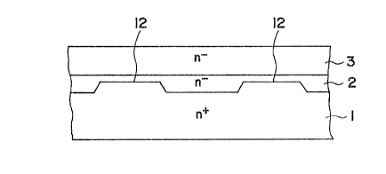
(5econd Embodiment)
Figure llB is a cross-sectlonal view of a light
detecting device of a second embodimen~ of -the presen~
inventlon.
In Figure ll~, the same symbols as Figure 4D show
th~ same elements as Figure 4Do
This light det~c~ing device is the same as the
firs~ embodiment except tha~ the n~-~ype InGa~s layer 2
is thinner in the outside of the p~-type InP lay2r 6.
In order to maklng partially thln the n~-type
InGaAs layer 2, for example, a convex part 12
surroundiny the aotiva area S is *ormed on the main
surface o~ the n~-type InP substrate 1, 2S shown in
,, , : : , ~ '
~: :' : . :
' ' :' :'
:',. . ' ~ , ~ : ' . :
~9~7~
13
Figure llA. The conve~ part 12 can be ea3ily formed by
making the InP substrate 1 selectively -thin by means of
~asks and etching technologyO
In this manner, when the n~-type InGaAs layer 2 is
formed on the InP substrate 1 having the convex par-t 12
so as to be 2O5 ~m thick in the active area S, the
upper surface of -the n~-type InGaAs layer 2 becomes
flat. And a light detec-ting device shown ln Figure llB
can be obtained by forming the n~-type InP layer 3 in
the same way as the first embodiment and forming a
trench 5 and diffusing impurities and forming an
antireflectlon film 9 and th~n ~orming electrode 10
and 11 in the same way as the first embodlment.
In such a light detecting device, since the n~-type
InGaAs layer 2 where pairs of electron and hole are
liable to be generated by irradiation of light is made
thln in the outside of the activs area S, the number of
carriers generated ln the outside of the depletion
layer ~s decreased. Thus, since the number of carriers
generated lnside the depletion layer is relatively
~ncreasad, lt is hard for the response characteristic
to be deteriorated in a range of high fre~uency.
~Third Embodiment)
Figure 12 is a cross-sectional view of a light
detecting device of a third embodiment of the present
inventlon, and the same s~mbols as Figure 4D show the
same elements as Figure 4D.
The light detecting device shown in F1gure 12 is
made diffsxent from the light detecting devi~e shown in
Figure 4D by having a p~-type diffusion layer 15 ~ormed
around~ the end face of ths light detecting device
wlthout havlng a trench 5 formed around the active area
S~
The reason why the trench 5 ls formed in the light
~ 35 detecting device shown in the ~lrst embodiment is that
it ls desired -to make the p~-type diffuslon layer 7
dePper than the p~-type InP layer 6 in the actlve area
.. ... . .
,.......... . , . ~
2 ~ 7 6
14
S. Namely, forming deeply the pt-type difEusion layer 7
after forming the trench 5 makes smaller the number of
carriers generated in the n~~type InGaAs layer 2 around
of the depletion layer.
As for reducing the dark current, since the same
effect as the first embodiment can be obtai~ed also
with the light detecting device shown in Figure 12, the
structure shown in Figure 12 is adequate for aiming at
reduction of the dark current.
(Other Embodiments)
In ~he above-men~ioned embodiments, an InP
substrate is used, on which an InGaAs layer and an InP
layer are formed, but the materials to be used are not
particularly limited to them. For example, also in case
that a photodlode made by forming an InGaAsP layer on
an InP substrate or a photodiode uslng GaAs or the like
~s used, since the dark current can be decrea~ed by
dlffusing an impurity of conductive type which is
opposite to the sub~trate in polarity toward the
ou~side o~ the photodiode, a light detecting device ran
b~ made small ln size~
And in the above-mentioned embodiments, by setting
thickness of the first silicon nitride film around the
active area S as 1/4 of the wavelength ~ of the ligh~
passing through the inside of it and setting the total
thickness of the first and second slllcon nitr~de films
4 and 8 a~ 1~2 of the ~, these fllms may be made act as
xeflection films. According to this method, an amount
of light incldent on the sP~con~uctor layer outside
the depletion layer is decreased and gen~ration of
electrons and holes in that area is suppressed, and as
a result the frequency vs. response characteristic is
uved.
In ~he above-mentloned embodiments, the first and
the second P~-type impurity doped layer 6 and 7 are
formed by thermal diffusion of impurity to non-doped
layer, but they may be formed by ion implantation.
.,~., .. : ............................. :
; ~ : - . ~ .
. . . . . .
21191 7~
Further, they may be formed by growing doped layer.