Note: Descriptions are shown in the official language in which they were submitted.
WO 93/0658~ PCr/US91/06601
2 li ~ 9 2 4 7
--1--
Description
Method For Writing Data To
An Electrophoretic DisplaY Panel
Technical Field
The present invention relates to a method
for operating an electrophoretic display panel
apparatus and, more particularly, to a method which
increases the speed with which information can be
written to an electrophoretic display panel.
Backqround Art
Electrophoretic displays (EPIDS) are now
well known. A variety of display types and features
are taught in several patents issued in the names of
Frank J. DiSanto and Denis A. Krusos and assigned to
the assignee herein, Copytele, Inc. of Huntington
Station, New York. For example, U.S Patent Nos.
4,655,897 and 4,732,830, each entitled ELECTROPHORETIC
DISPLAY PANELS AND ASSOCIATED METHODS describe the
basic operation and construction of an electrophoretic
display. U.S. Patent No. 4,742,345, entitled
ELECTROPHORETIC DISPLAY PANELS AND METHODS THEREFOR,
describes a display having improved alignment and
contrast. U.S. Patent No. 4,833,464 entitled
ELECTROPHORETIC INFORMATION DISPLAY (EPID) APPARATUS
EMPLOYING GREY SCALE CAPABILITY relates to an EPID
with the capability to display pixels of varying grey
scale intensity. This patent recognizes, inter alia,
that the duration of application of a voltage gradient
at a particular pixel location effects the quantity of
pigment particles at that location. Hence, by
controlling the time duration of the write pulse one
can achieve grey scale capability - the shorter the
pulse, the lighter the line.
W093/~58~ - PCT/US91/06601
2~19247 -2-
The display panels shown in the above-
mentioned patents operate upon the same basic
principle, viz., if a suspension of electrically
charged pigment particles in a dielectric fluid is
subjected to an applied electrostatic field, the
pigment particles will migrate through the fluid in
response to the electrostatic field. Given a
substantially homogeneous suspension of particles
having a pigment color different from that of the
dielectric fluid, if the applied electrostatic field
is localized, it will cause a visually observable
localized pigment particle migration. The localized
pigment particle migration results either in a
localized area of concentration or rarefaction of
lS particles depending upon the sign and direction of the
electrostatic field and the charge on the pigment
particles. The electrophoretic display apparatus
taught in the foregoing U.S. Patents are "triode-type"
displays having a plurality of independent, parallel,
cathode row conductor elements or ~lines~ deposited in
the horizontal on one surface of a glass viewing
screen. A layer of insulating photoresist material
deposited over the cathode elements and photoetched
down to the cathode elements to yield a plurality of
insulator strips positioned at right angles to the
cathode elements, forms the substrate for a plurality
of independent, parallel column or grid conductor
elements or "lines" running in the vertical direction.
A glass cap member forms a fluid-tight seal with the
viewing window along the cap's peripheral edge for
containing the fluid suspension and also acts as a
substrate for an anode plate deposited on the interior
flat surface of the cap. When the cap is in place,
the anode surface is in spaced parallel relation to
W093/06585 a 1-1 9 2 4 7 1~ PCT/VS9l/0660l
both the cathode elements and the grid elements.
Given a specific particulate suspension, the sign of
the electrostatic charge which will attract and repel
the pigment particles will be known. The cathode
element voltage, the anode voltage, and the grid
element voltage can then be ascertained such that when
a particular voltage is applied to the cathode and
another voltage is applied to the grid, the area
proximate their intersection will assume a net charge
sufficient to attract or repel pigment particles in
suspension in the dielectric fluid. Since numerous
cathode and grid lines are employed, there are
numerous discrete intersection points which can be
controlled by varying the voltage on the cathode and
grid elements to cause localized visible regions of
pigment concentration and rarefaction. Essentially
then, the operating voltages on both cathode and grid
must be able to assume at least two states
corresponding to a logical one and a logical zero.
Logical one for the cathode may either correspond to
attraction or repulsion of pigment. Typically, the
cathode and grid voltages are selected such that only
when both are a logical one at a particular
intersection point, will a sufficient electrostatic
field be present at the intersection relative to the
anode to cause the writing of a visual bit of
information on the display through migration of
pigment particles. The bit may be erased, e.g., upon
a reversal of polarity and a logical zero-zero state
occurring at the intersection coordinated with an
erase voltage gradient between anode and cathode. In
this manner, digitized data can be displayed on the
electrophoretic display.
~ 4 ~ ~ 2 47
An alternative EPID construction is described
in U.S. Patent No. 5,053,763 issued on October l, l99l
and entitled DUAL ANODE FLAT PANEL DISPLAY APPARATUS,
which relates to an electrophoretic display in which the
cathode/grid matrix as is found in triode-type displays
is overlayed by a plurality of independent separately
addressable "local" anode lines. The local anode lines
are deposited upon and align with the grid lines and are
insulated therefrom by interstitial lines of photoresist.
The local anode lines are in addition to the "remote"
anode, which is the layer deposited upon the anode
faceplate or cap as in triode displays. The dual anode
structure aforesaid provides enhanced operation by
eliminating unwanted variations in display brightness
between frames, increasing the speed of the display and
decreasing the anode voltage required during Write and
Hold cycles, all as explained in U.S. Patent No.
5,053,763.
A commonly sought objective for EPIDS of both
triode and tetrode types, and for digital display
equipment and computer and digital apparatus in general,
is increased speed of operation. With respect to
displays, it is desirable for the display to be able to
write, erase and edit the displayed image as quickly as
possible in response to operator input and computer
processing. For example, when a computer with a visual
output device for displaying character information, such
as a CRT, is used as a word processor, if the writing and
erasure of displayed information is not fast enough, it
will slow the operator of the word processor in the
completion of his task. Even though the computer memory
and processing unit can operate at speeds far exceeding
W093/~ ~5 PCT/US91/0~01
2 ~ ~ ~ 2 4 7
the capacity of a human user, if the input and output
devices through which the computer communicates with
the user are slow, the computer and the user must wait
for the output devices. Thus, if a word processor
user is paging through a document at high speed, a
slow visual output device may well slow the speed of
paging below that at which the user and/or the
computer could potentially perform.
In EPIDS and in other display apparatus,
because there are a plurality of pixels arranged on a
coordinate grid or matrix, and because the pixels must
be independently addressable, display operations are
frequently conducted at the pixel level, e.g., each
pixel is sequentially written to. Sequential
operations are intrinsically time consuming, in that
the prior operation must be completed before the
subsequent can be started. Further, even though the
writing of a single pixel can be done very quickly,
there are such a large number that even a small write
time is significant. A process for independently
controlling individual pixel display whereby a degree
of parallel display processing is accomplished is
described, e.g., in U.S. Patent No. 4,742,345, wherein
display information pertaining to an entire line of
pixels, i.e., On or Off, is accumulated in an
accumulator or register during a first phase, placed
in parallel into a latch array in a second phase and
placed in parallel on one of the coordinate qrids in a
third phase. Placing the display information onto one
of the coordinate line sets, e.g., the grid lines
which may be oriented in the vertical direction, has
been termed "loading" the data on the grid. When the
bits of information (voltages corresponding to logical
"1" and "O") are placed or "loaded" on, e.g., all the
W093/~58~ 2 4 7 PCT/~S91/06601
--6--
vertical coordinate lines, a single horizontal line
can be written by enabling that line, i.e., by placing
a voltage corresponding to a logical "l" on that
horizontal line. The operation of placing an enabling
voltage upon the line to be written, in this case a
horizontal cathode line, has been referred to as
"writing the line". of course, this line-by-line
writing method also has a upper limit of speed.
With respect to EPIDS, one factor which
contributes to the speed with which the display can
operate is the speed with which the pigment particles
can travel through the electrophoretic fluid under the
influence of a particular voltage gradient. Pigment
particle migration speed depends, inter alia, upon
particle size and electrophoretic fluid viscosity. In
addition to the particle speed, there is also the
factor of spatial distribution within the EPID
envelope, i.e., because the particles are in
suspension they are distributed, prior to being
exposed to voltage gradients, relatively evenly within
the fluid envelope. Accordingly, there is a range of
particle proximity to the "target" element, the target
element being that element to which the particles are
sought to be directed to perform an operation, such as
write or erase.
These speed and proximity factors in EPIDS
are utilized in U.S. Patent No. 4,833,464 to control
pixel display intensity or grey scale. Namely, if a
voltage gradient of shorter or longer duration is
applied, fewer or greater particles will accumulate at
the "target" electrode thereby ~ffecting pixel
intensity, i.e., the greater the number of particles,
the greater the intensity. Note that pixel intensity
is discernable at both sides of the typical EPID so
W093~58~ PCT/~1S91/06601
~ ~19~47
--7--
that an intense accumulation of e.g., light colored
particles, on one face of the EPID is accompanied by a
correspondingly intense lack of light particles on the
other face, which, in all probability, will appear
dark due the selection of a dark solution or
background for the light colored particles. Thus
writing a character on one faceplate of an EPID
results in its reverse image being written on the
other plate. The writing of a blank character may be
termed selective character erasure.
It is an objective of the present invention
to provide a method for operating an EPID having any
particular pigment particle size, electrophoretic
fluid viscosity, electrode arrangement and operating
voltage levels, such that the speed of operation is
increased.
Disclosure of the Invention
The problems and disadvantages associated
with conventional methods of operating electrophoretic
displays are overcome by the present inventive method
for decreasing the time to write a frame of display
data composed of a plurality of lines of displayable
pixels on an electrophoretic display requiring a
minimum time period for a line to be fully written. A
set of at least two adjacent lines is written in a
shortened period shorter in duration than the minimum
period. The elements of the line set are then shifted
such that the set contains at least one new line and
at least one old line. The shifted line set is then
written in a subsequent shortened period following the
step of shifting. The set is repeatedly shifted and
written in the foregoing fashion until the frame is
completely written.
- 7a - 27 ~ g 2 4 7
According to a further broad aspect of the present
invention there is provided a method for decreasing the time to
write a frame of display data composed of a plurality of lines of
displayable pixels on an electrophoretic display requiring a
minimum time period for a line to be fully written. The method
comprises selecting a shortened period which is shorter in
duration than the minimum period. A line set of at least two
adjacent lines is written in the shortened period. The lines of
the said line set are then shifted such that the line set
contains at least one new line and at least one old line. The
shifted line set is written in a subsequent shortened period
following the step of shifting and the steps of shifting the
lines and writing the shifted lines are repeated until the frame
is completely written.
E3
W O 93/0658~ PC~r/US91/06601
~ 9 ~ 4 7 -8-
Brief DescriPtion of the Drawinqs
For a better understanding of the present
invention, reference is made to the following detailed
description of an exemplary embodiment considered in
conjunction with the accompanying drawings, in which:
FIG. 1 is a cross-sectional view of a
typical triode-type EPID showing the essential
electrical components thereof.
FIG. 2 is a simplified schematic diagram
illustrating an addressable display matrix comprised
of horizontal and vertical elements, such as, a
plurality of cathode lines and a plurality of grid
lines, driven by display drivers, as would be used in
known EPID devices like that shown in FIG. 1.
FIG. 3 is a simplified schematic diagram
illustrating circuitry for controlling the x and y
display drivers illustrated in FIG. 2.
FIG. 4 shows a character which could be
displayed upon an x-y matrix using the circuitry and
apparatus as illustrated in FIGS. 1-3, as controlled
and operated in accordance with the method of the
present invention.
FIG. 5 is a flowchart showin~ a method for
EPID writing in accordance with the present invention.
Best Mode for Carryinq Out The Invention
FIG. 1, which is taken from U.S. Patent No.
4,732,830, shows an electrophoretic display 10 as is
now known in the art. The display 10 has an anode
faceplate 12 and a cathode faceplate 14 which are
sealably affixed on either side of an interstitial
spacer (not shown) to form a fluid-tight envelope for
containing a dielectric/pigment particle suspension or
electrophoretic fluid. The faceplates 12 and 14 are
typically flat glass plates upon which are deposited
9 ~ 47
conductor elements to comprise the situs of the
electrostatic charge for inducing motion of the pigment
particles 16 in the electrophoretic fluid. The
techniques, materials and dimensions used to form the
conductor elements upon the faceplates and the method for
making and using EPIDS, in general, are shown in U.S.
Patent Nos. 4,655,897; 4,732,830 and 4,742,345.
Known EPIDS, as depicted in FIG. 1, for
example, have a plurality of independent, electrically
conductive cathode lines 18, shown here as horizontal
rows, deposited upon the cathode faceplate 14 using
conventional deposition and etching techniques. Of
course, the orientation of the cathode lines 18 depends
upon the orientation of the screen, which, if rotated 90
degrees, would position the cathode lines vertically.
Thus, the cathode lines are arbitrarily defined as
horizontal or in the x-axis. It is preferred that the
cathode elements 18 be composed of Indium Tin Oxide (ITO)
as set forth in U.S. Patent No. 4,742,345. A plurality
of independent grid conductor lines 20 are superposed in
the vertical (parallel with the y-axis) over the cathode
elements 18, i.e., at right angles thereto, and are
insulated therefrom by an interstitial photoresist layer
22. The grid elements 20 may be formed by coating the
photoresist layer 22 with a metal, such as nickel or
chrome, using sputtering techniques or the like, and then
selectively masking and etching to yield the intersecting
but insulated configuration shown in FIG. 1. Each
cathode and grid element 18, 20 terminates at one end in
a contact pad, or is otherwise adapted to permit
connection to display driver circuitry. An anode 26 is
formed on an interior surface of the anode faceplate 12
by plating with a thin layer of conductor material, such
as, chrome.
The foregoing components have been previously
described in prior patents and applications of the
present Applicants. In addition to these teachings, the
,~,, .
- lo - ~ 2 ~7
benefits and operation of an EPID having a local anode
have been recognized and described in the above-mentioned
U.S. Patent No. 5,053,763 by the present Applicants. The
present inventive method could find application in any of
these disclosed devices.
FIG. 2, also taken from U.S. Patent No.
4,732,830, shows, in the simplest schematic form, how the
cathode 18 and grid lines 20 comprise an addressable x-y
matrix allowing pixels at the intersection points to be
selectively displayed. Each horizontal 18 and vertical
20 line has an associated amplifier/driver 24R and 24C,
respectively, for impressing either a logical "1" or "0"
thereon, such that when both are "1" at an intersection,
that intersection is written. The horizontal lines have
been labeled Rl...R2200 to signify that 2200 display
lines 18 or rows would typically be present. 1700
vertical lines 20 or columns are common, as depicted by
the labels Cl...C1700.
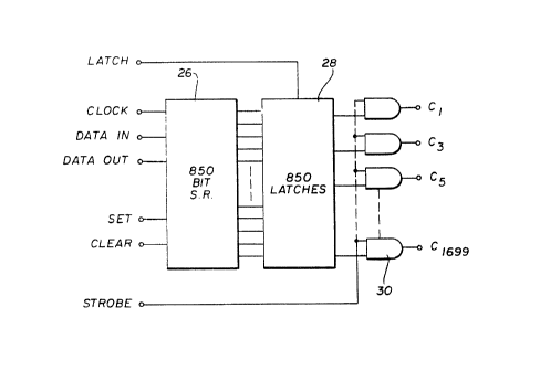
FIG. 3, taken from Patent No. 4,742,345, shows
exemplary circuitry for supplying input data to the x and
y drivers, 24R and 24C. As explained fully in Patent No.
4,742,345, a large capacity, composite, serial-to-
parallel register 26 may be used as a buffer for
collecting a large number of bits of display data, e.g.,
850 bits. After sequentially clocking data into the
register 26 and filling it to capacity, the data
W093/06585 PCT/~S91/0~01
4 7
--11--
is latched in parallel into a latch array 28 having an
equal capacity. The data is then strobed into the
- display driver amplifiers 24 through a plurality of
AND gates 30. Data may be accumulated in the serial
register while the transfer from latch array 28 to
drivers 24 occurs. In FIG. 3 the output of the AND
gates are labelled with odd number columns l through
1699. The data for even number columns would be
supplied, in this case, by a twin circuit disposed on
the cathode faceplate opposite to that for the odd
columns. This configuration prevents overcrowding of
electrical connections to the grid lines as explained
in Patent No. 4,742,345. Once the column data is
supplied to all columns, a row can then be written by
sending a "l" along the row or cathode 18 to be
written. The row "l" in combination with any column
"l" will cause the writing of a pixel at the
intersection thereof, i.e., a voltage gradient at that
point sufficient to cause a visually observable
migration and agglomeration of pigment particles 16.
The proportions of the grid 20 and cathode
18 lines as shown in FIGS. l and 2 have been greatly
enlarged for the purposes of illustration. In
operational displays, the grid 20 and cathode 18 lines
are very thin and elongated. A workable panel would
have a large number of intersections, e.g., 2,200 X
1,700 or a total of 3,740,000 separately addressable
intersection points in a panel approximately 8" X ll".
For ease of illustration, only a few cathode lines 18,
and grid lines 20 are depicted. Additional
illustrations of electrophoretic displays, their
components and electrical circuitry can be seen by
referring to U.S. Patents Nos. 4,742,345 and
WOg3/~58~ PCT/US91/06601
~ ~9~4? -
-12-
4,772,820, each being awarded to the inventors herein
and which are incorporated by reference herein.
FIG. 4 illustrates a character, i.e., the
letter "T" written on a EPID as described above in
reference to FIGS. 1-3 by utilizing the algorithm
flow-charted in FIG. 5. In accordance with the
present inventive method, it has been observed that
the writing time of the EPID can be reduced by
simultaneously writing more than one line at a time.
That is, in the above-described previously known
EPIDS, an entire set of column data for a particular
row is impressed upon the columns, e.g., the grid
lines. A single row is then enabled with a logical
"1" and thereby written. The next set of column data
is loaded onto the grid lines and the next row is
enabled or written. This goes on sequentially until
the entire screen is written. There is a certain
period required for the pigment particles to migrate
through the electrophoretic fluid to their "write"
position, i.e., to make an agglomeration sufficient in
size to be clearly visible. Therefore each row in
past operation had to be held in the lo~ical "1" state
for the required writinq period or writing cycle time.
In accordance with the present invention, if a set of
rows greater than one row, e.g., two rows, is enabled
simultaneously for a period approximately one-half as
long in duration as was previously done, then the two
rows will both be dimly written with the same display
information in one half the cycle time. For instance,
if column data for row l is loaded and rows 1 and 2
are written, both row 1 and row 2 will be dimly
written with row l display information. If new
column data, i.e., for row 2, is loaded and the row
set is shifted down one and written, i.e., row set 2
W093/~585 _l3_ PCT/I'S91/06601
and 3 are written using row 2 data, the first row
which was half-written will be left untouched. The
second row, however, will be fully written assuming
the new column data associated with row 2 is the same
as that associated with row l. Row 3 is also dimly
written with row 2 data. Thus, by partially writing
subsequent overlapping row sets with shortened writing
cycles, the entire display can be written much faster
than if single rows are sequentially fully written.
This row set writing strategy depends upon the fact
that there is repetition in the pixel pattern from one
row to the next. In fact, there is a hiqh probability
of that condition occurring. Because of high line
density in the EPIDS in question, the number of lines
comprising a single character is great. For example,
a 70 line X 25 line matrix with 1750 pixels may be
used as the area for expressing a single character.
As such, the pattern of pixels comprising the common
characters is very repetitive. Fig. 4 illustrates
this principle using a matrix of only 22 X 22 lines,
i.e., those lines centrally located within the entire
29 X 31 line matrix depicted. The top of the "T"
begins at (r5,c5) and ends at (r9,c26). The
significance of the X's on row 5 will be explained
below. The stem of the "T" starts at (rlO,cl3) and
ends at (r26,cl7). As can readily be seen, the top of
the "T" is composed of 5 identical rows of pixels and
the stem of the "T" is composed of 17 identical rows
of pixels. The "T" depicted in FIG. 4 is an example
of applying the present inventive method in writing in
two row sets at one half the normal write cycle time
(twice the writing speed). Specifically, one would
execute the following steps in order to display the
"T" shown in FIG. 4.:
W093/~58~ PCT/US91/06601
-14
. 4 7 -;
Load cl-c29 with data for rl
(O,O,O,O,O,O,O,O....... o)
Write rl and r2 simultaneously (put "1" on rl and r2)
Load cl-c29 (the grid lines) with data for r2
( O , O , O , O , . ~ ~ ~ )
Write r2,r3
Load grid with r3 data
Write r3, r4
Load grid with r4 data
Write r4,r5
Note: for the purposes of this example, r5
has been selected as the first line that has ~ls" or
written pixels in it and it should be the first line
of the "top" of the "T". Due to the fact, however,
that r5 is a transition line, i.e., a transition from
non-written to written pixels, it will not be
completely written and instead will only be dimly
written or half written. This is so because each
write cycle, since it is at twice the speed as a
normal cycle, only "half writes" the information.
The next cycle is necessary to fully write the
information, but only if the next cycle uses the same
data. In the case of a transition line, succeeding
rows have different data. Since there are so many
lines of pixels in operable displays, the loss of
small numbers of transition lines and/or pixels does
not cause a significant loss in readability.
Returning now to the writi~g process:
Load grid with r5 data
(0,0,0,0,1,1,1,1,1,1,1,1...1,0,0,0)
Write r5,r6
W093/~58~ PCT/US91/06601
2~ 2 4 7
-15-
Load grid with r6 data (same as r5 data)
Write r6, r7 (since r6 was previously "half" written
with r5 data in the prior cycle and since the r5 data
was the same as the r6 data, r6 is written completely
on the subsequent cycle.)
Load r7 data
Write r7,r8
Load r8
Write r8,r9
Load r9
Write r9,rlO (rlO is another partial transition line,
i.e., it is the transition from the top of the ~T" to
the stem of the "T". Since the rs data is written on
line 10, a portion thereof, i.e., that which should
contain non-written pixels - the X's - will be dimly
or half written.)
Load rlO
Write rlO,rll
repeats until row 26 where:
Load r26
Write r26,r27 (constitutes another transition line)
Load r27
Write r27, r28, etc.
The foregoing should illustrate one
embodiment of the present inventive method. Further,
it can be understood that in lieu of two line set
writing, three, four, or more lines can be written
simultaneously with corresponding increases in speed
and in transition lines which will be of varying
intensity depending upon the number of repetitions of
writes to those transition lines. For example, in
WO 93/0658~ PCr/VS91 /06601
~ 247 ~ -16-
four line set writing, when a transition from blank to
written pixels occurs, there are three transition
lines, the first being the dimmest and the last, the
darkest. The fourth line written will be fully
written. Similarly, in a transition from written to
non-written pixels, there will be three transition
lines, the first being the darkest and the last the
dimmest. The fourth line will be non-written. Of
course, in four line set writing, the benefit of
increasing writing speed over the normal speed would
be utilized to produce a fourfold increase in speed.
FIG. 5 is a generalized flowchart of the
steps of the present inventive method for operating an
EPID in a multi-line write mode. It would be expected
that operator selection of display writing speed
would be offered so that the operator can choose the
speed and clarity. This sort of selection is
presently offered to operators upon printing on dot-
matrix printers, i.e., enhanced printing has greater
pixel density but takes longer to print. Accordingly,
the operator flrst enters the number of lines to be
written in each write cycle 32. From this input the
write cycle time (writing speed) is adjusted 34. The
greater the number of lines simultaneously written in
each write cycle, the faster the writing speed. Of
course, the operator input could be expressed as a
selection of writing speed, wherein the operator would
select from a range of speeds corresponding to the
number of lines simultaneously written. The flowchart
shown in FIG. 5 pertains to the display of a single
complete image (frame) on the EPID. This algorithm
would be utilized over and over under the control of
programming at the next higher level. The operator
would not be queried as to the operating speed on each
W093/~58~ ~ 7 ~ ~ ~ 4 7 PCT/~S91/06601
frame displayed. Information of that type would be
initially set by query or default then changed by
interrupt if desired. Having determined the line set
size for writing, the writing is begun at the first
row 36. (Of course, it would be equally feasible to
load rows with data and write columns.) The processor
then enters a loop wherein data for the current row is
loaded onto the column lines (here grid lines) 38.
The data is simultaneously written on the current row
and the next x-l rows by enabling those rows with a
logical "1" 40, x being the number of rows in the
write set selected. Thus, on the first write cycle in
a 4 line set write mode, row 1 and the next (4-1) or 3
rows, i.e., rows 2, 3 and 4 are written. Note that
the "1" state may correspond to a variety of voltages
depending upon the EPID in question, e.g., whether the
EPID is a triode or tetrode. A voltage of 0 volts has
been used to enable writing in triodes and, in those
instances represents a logical "1" or enable state.
The row set is written for a write cycle time that has
been adjusted by the size of the row set (divided by).
This is continued until all rows are written 42,44,
whereupon control is returned to the next higher level
in the program. Of course other line writing
sequences could be employed using a multi-line write
strategy, for example, vertical lines can be written
from left to right or -right to left, horizontal lines
could be written from bottom to top or from the middle
to the outer periphery, etc.
It should be understood that the embodiments
described herein are merely exemplary and that a
person skilled in the art may make many variations and
W093/0658~ PCT/~IS91/0660l
211~24~7
-18-
modifications without departing from the spirit and
scope of the invention as defined in the appended
claims.