Note: Descriptions are shown in the official language in which they were submitted.
2119~01 -
COMPUTER SYSTEM WHICH OVERRIDES WRITE
PROTECTION STATUS DURING EXECUTIO~ ~N
SYSTEM MANAGEMENT MODE
The invention relates to computers having system
management mode operations, particularly where the
memory for the system management mode is located in the
main memory space of the computer and accessible by
conventional applications and thus must be write
protected.
2.
Microprocessor-based computer systems have been
increasing in performance at a tremendous rate. Much
of this increase has been based on the improvements in
the microprocessor itself. For example, clock speeds
are reaching those previously used only by mainframe
computers. However, affordable memory device
performance has not been increasing at the same rate.
Indeed, dynamic random access memory (DRAM) performance
has flattened out recently, with the majority of the
effort being concentrated on increasing device storage
size. Thus main memory has become a bottleneck.
Cache memory systems, where a small amount of very
fast, expensive static RAM is used to store copies of
the data, have made the problem somewhat less severe,
but the designs are very complicated and expensive.
Further, the poor memory performance returns when
access must be made to main memory. So there still is
a need to improve the performance of the main memory
system.
2119~1
Page mode memory devices provide one way to
increase memory system performance. If consecutive
accesses are made to the same row address, referred to
as the same page, only column addresses need be
provided. This allows a dramatic reduction in cycle
time for those cases, referred to as page hits. This
is a quick gain and relatively easily made by itself,
but more performance is alwa~s desired.
In many processors, the address is provided before
the data portion of the cycle. This is referred to as
pipelining and allows a performance increase in the
memory systems. All of the address decoding can be
started before the data portion begins, so that
partially parallel operations can occur.
In most cases this overlap is somewhat minimal,
one or two clock cycles, as the related systems cannot
handle much more complexity. For example, the memory
controller is conventionally built as a synchronous
controller, based on a major state machine to control
events and advancing on the processor clock edge. As
the complexities of the microprocessor and the computer
system increase, the conventional memory controller
design becomes very limiting. It is exceedir.gly
difficult to build a major state machine to handle all
the possible cases. The complexity is daunting, if not
overwhelming. As a result, numerous potential
performance improvements have to be limited. Usually
this means that any pipelining is limited and there are
very few parallel operations. While some designs--
allowed write operations to be posted, this justfurther increased complexity in other ways. As a
result, some other feature was sacrificed, so potential
gains were lost.
Memory system performance is also a trade off
between cost and speed. While conventionally 80 ns
2~ t9~t
DRAMs have been used, 60 ns devices are available,
though at a slightly higher cost. While prior memory
controllers could utilize differing speeds of DRAMs,
allowing the user to make the speed versus cost
tradeoff, a mixed speed system did not obtain any
benefits. The memory controller could use different
speed DRAMs, but only one actual speed of operation was
allowed in the system. The memory controller thus ran
at the speed of the slowest of the installed DRAMs.
This did not allow the user to have fast memory areas,
such as the base memory area, and slow memory areas,
such as extended memory locations in the main system
memory controlled by the memory controller. This
limitation arose again because of the complexities of
memory controllers.
Thus there are memory system performance gains
that could be achieved, but conventional design
limitations render them only potential, not practical.
Therefore it is clearly desirable to have a memory
controller which makes maximum use of processor address
pipelining, can run numerous cycles concurrently in the
greatest number of cases and can effectively use
different speed memory devices.
Additionally, certain microprocessors, such as the
80386SL and the 80486SL from Intel Corporation have
included a mode referred to as system management mode,
which is entered upon receipt of an SMI or system
management interrupt. Recently the P5 or Pentium
processor from Intel has added this feature. The-~5 is
a very high performance microprocessor having a
superscalar architecture and integrated and separate
code and data caches. The data bus is 64 bits wide and
8 parity bits are provided. The data cache is a write-
back design having a 32 byte line width.
21 1!34~ 1 -
An SMI pin is used to enter SM mode and a signal
referred to as SMIACT* is provided by the P5 or Pentium
to indicate operation in SM mode. When an SMI is
asserted, an Intel microprocessor maps a portion of
memory referred to as the system management memory
(SMRAM~ into the main memory space. The entire CPU
state is then saved in the SMRAM in stack-like, last
in/first out fashion. After the CPU state is saved,
the microprocessor begins executing an SMI handler
routine, which is an interrupt service routine to
perform specific system management tasks, like reducing
power to specific devices. While the routine is
executed, other interrupt requests are not serviced,
and are ignored until the interrupt routine is
completed or the microprocessor is reset. When the SMI
handler completes its task, the CPU state is retrieved
from the SMRAM, and the main program continues.
In the first processors to use SMIs, the Intel
Corporation 80386SL and 80486SL microprocessors, the
SMRAM is mapped into the main memory space between
30000h and 3FFFFh. Data regarding the CPU state is
stored starting at 3FFFFh going down like a
conventional stack. After the CPU state is saved in
the SMRAM, the microprocessor starts the SMI handler at
memory address 38000h located in the SMRAM space. In
the 80386 and 80486 microprocessor generations, the SMI
start address is stored in a non-accessible register so
that it cannot be changed by the programmer.
Similarly, the use of the memory space between 30~QOh
and 3FFFFh is preset into the microprocessor and
unchangeable. Although this placement of the SMRAM and
starting address is stable and known, it is often
inconvenient. Any data stored in the main memory space
between 30000h and 3FFFFh before the SMI is asserted is
likely to be overwritten by the SMI handler and lost,
21134~ -
unless hardware is developed which maps in special
memory and maps out conventional memory. This mapping
requirement has the problem of requiring extra logic
and forces abrupt changes in memory contents
necessitating flushing of any cache memory system.
This has a cost and performance drawback. If the
mapping is not performed, the software must be
carefully designed around the memory space used by the
SMRAM in order to prevent inadvertent loss of data.
To remedy this inconvenience, the Pentium or P5
microprocessor permits the SMI handler starting address
and the location of the SMRAM space to be changed by
the user. Under the Pentium design, the SMI starting
address stored in the microprocessor register is
initially set to the conventional 30000h value.
Consequently, when the first SMI is asserted, the SMI
handler starts at address 38000h. While the SMI
handler routine is executing, however, it may provide a
different area of memory to be used as the SMRAM. This
new SMRAM may start at any location in the main memory
space chosen by the programmer. The SMRAM comprises a
64 kbyte block beginning at the new SMRAM start
address. When the SMI handler finishes, the new
starting address replaces the old starting address in
the microprocessor's SMI starting address register.
When the next SMI is asserted, the microprocessor
maps the new 64 kbyte block of memory into the main
memory space as the SMRAM, and starts the SMI handler
at the new starting address at the midpoint of the_new
SMRAM. For example, during the first SMI service
routine, the programmer may change the SMRAM starting
point from 0300GOh to lOOOOOh. When the SMI is next
asserted, the microprocessor maps the SMRAM into main
memory space between lOOOOOh and lOFFFFh. The
microprocessor then references address 108000h for the
211~Ql
SMI handler. This feature thus allows the programmer
to choose a more convenient location in the main memory
for the SMRAM.
Although the ability to relocate the SMRAM
provides a convenient option to the programmer, it
presents a problem. Because of the very high level of
code placed in the SMRAM and its sensitive nature, it
is very desireable to write protect this area of memory
when it is located in the main memory space to prevent
inadvertant overwriting of the code. Many problems
could result if the system management code was
overwritten, as the system would not respond properly
to an SMI. When the SMRAM was located external to the
main memory space, this was not a problem as the
mapping of the memory to an area outside of the normal
main memory space prevented inadvertant writes to the
area and so write protection was not necessary. So
when the SMRAM area is in the main memory space it must
be write protected.
But write protecting this block adds a further
problem. Conventionally write protection is done based
on physical addresses. Thus once write protected, the
area would stay write protected until specific
instructions are performed. The processor could not
store the internal state values upon entry into the
system management mode as those instructions would not
be performed prior to the automatic state storage
operations. This would prevent a proper restoration of
the machine state. Further, the system management_code
would not be able to use a reserved area in the SMRAM
for its own data storage until after the special
instructions are performed. The area would be write
protected and thus could not be used for scratchpad or
more permanent storage. Using memory elsewhere might
not be possible as that would possibly interfere with
-- 21 1 9401
applications code present at those locations. This write
protect bit could also prevent write operations to certain
locations once system management mode was entered.
Therefore it is desirable to resolve this write protection
problem with SMRAM so that the SMRAM can safely be placed in
main memory and yet operate properly during system management
mode operations.
A memory controller according to the present invention
makes maximum use of any processor pipelining and allows a large
number of cycles, up to five, to be running concurrently on the
computer system. This allows a marked improvement in the
performance of the memory system.
One aspect of the invention provides a method for operating
a computer system management mode which is operable in the main
memory space of the computer, comprising the steps of providing
an indication that a portion of the main memory space is write
protected, determining when system management mode is active and
overriding the indication of write protection when system
management mode is determined to be active, so that the main
memory space is writable.
Another aspect of the invention provides a computer system
having a system management mode which is operable in the main
memory space of the computer, the computer system comprising
means for providing an indication that a portion of the main
memory space is write protected, means for determining when
system management mode is active and means for overriding the
indication of write protection when system management mode is
determined to be active so that the main memory space is
writable.
More particularly, the primary way this improvement is
obtained is by moving the memory control functions from a large,
complicated master state machine to a plurality of simple,
interdependent state machines. Basically each state machine is
responsible for one small portion of the overall operation,
generally one specific function. As each state machine reaches
a point where it has completed its function, it notifies a
related state machine that it can now proceed on its task and
21 19401
7A
proceeds to wait for its next start or proceed indication. The
second state machine operates in a similar fashion. This is
repeated until a complete cycle is performed. But the state
machines responsible for the earlier portions of a cycle, such
as address and command decode, have started their tasks on the
next cycle before the state machines responsible for
the later portions of the cycle have completed their
tasks. Thus the looser relationship allows each state
machine to advance as far as possible in each cycle,
2 ~
until it reaches a point it needs another signal to
proceed. This interdependent nature therefore allows
very efficient handling of pipelined conditions.
The memory controller is further logically
reorganized from a conventional case. The system
memory is not located off an intermediate or host bus,
but is located directly off the processor bus. The
host bus is also located off the processor bus. Thus
the three buses form a three point connection. A data
buffer is located at this three point connection and is
capable of handling data simultaneously on its three
buses. The number of potential data routes is thereby
increased over the conventional case, where all
processor-memory operations need the use of the host
bus, interfering with processor-host bus operations.
With data capable of going on two separate paths,
opportunities for concurrency are increased.
The memory controller is logically organized as
three main blocks, one called the front end being
connected to and responsible for processor bus
interaction. A memory block is provided to handle
interaction with the actual memory devices and
communicates with the front end block to indicate cycle
start and completion. Similarly, a host block is
provided to handle host bus interaction and also
communicates triggering events to the front end block.
The front end block decodes a cycle, determines
whether it goes to the memory or the host bus and
initiates the proper block. The front end block is
then free to work on the next cycle, so pipelining is
readily handled. If the next cycle is intended for the
other of the memory or the host bus, that block can be
activated and it begins its operations. Now full
concurrency is developed. The front end block is free
to decode yet another cycle, assuming one has been
2 ~
provided by the processor. Thus even more pipelining
can be developed. In the preferred embodiment an EISA
bus is developed from the host bus. As write
operations can be posted from the host bus to the EISA
bus, it is apparent that even more concurrency can be
obtained if an EISA-intended write operation is
interposed.
The arrangement of the memory controller as a
plurality of state machines simplifies this
concurrency. Fewer states are needed in total as the
possibilities are handled individually rather than as a
group. Thus the overall complexity of the memory
controller is greatly reduced, down to a manageable
size, yet pipelining and concurrency are obtained and
maximized.
In addition, the flexibility provided by the
plurality of state machines also allows the memory
controller to util~ze differing speed memory devices,
such as 60 ns and 80 ns, on an individual basis, with
the memory controller running each memory device at its
full designed rate, not the lowest of the rates in the
memory system. The speed of the memory is stored for
each 128 kbyte block of memory. This stored value is
then used when the memory cycle is occurring to
redirect a state machine, thus accomplishing a timing
change of the memory devices. As this value is
available for each 128 kbyte block, each memory device
can be operated at its full speed.
Further, the memory controller includes logic 50
that when system management mode is active, as
indicated by the SMIACT* signal, write protection is
overridden. In this manner the SMRAM can be located in
the main memory, in a region defined as write
protected, and yet when system management mode is
entered, the processor can store the internal state and
2119~1
the system management code can freely operate in the
SMRAM area without restrictions. This allows
transparent system management mode and normal mode
operations.
Therefore a memory controller according to the
present invention makes maximum use of any address
pipelining provided by the processor, can run numerous
cycles concurrently and dynamically adjusts its
operation for differing speed memory devices. This is
- 10 done without extreme complexity, so that reliable
operations under all possible operating conditions can
be more easily determined. Further, system management
code can be located in a write protected area of main
memory and yet be utilized as fully writable memory
during system management mode operation.
A better understandinq of the present invention
can be obtained when the following detailed description
of the preferred embodiment is considered in
conjunction with the following drawings, in which:
Figure 1 is a block diagram of a computer system
incorporating the present invention;
Figure 2 is a block diagram of the system board of
Figure 1;
Figure 3 is a block diagram of the input/output
board of Figure l;
Figure 4 is a block diagram of the processor board
of Figure 1; __
Figure 5 is a more detailed block diagram of
portions of the processor board of Figure 4;
Figure 6 is block diagram of the address/control
buffer of Figure 4;
Figures 7, 8 and 9 are block diagrams of the data
buffer of Figure 4;
2~13~
Figure 10 is a block diagram of the major portions
of the memory controller of Fig.4;
Figures 11-22, 24-34, 37-39, 42 and 44-50 are
state machine diagrams for a number of the state
machines in the memory controller of Figure 4;
Figures 23, 35, 36, 38A-38I, 40, 41, 43 and 51 are
schematic diagrams of portions of the memory controller
of Figure 4 used with various state machines; and
Figures 52-69 are timing diagrams of various
cycles of the memory controller of Fig. 4;
DETAI~ED DE8CRIPTION OF THE PRE~ERRED EMBODIMENT
Referring now to Figure 1, a computer system C
according to the preferred embodiment is shown. A
processor board P contains the processor, cache memory
and main memory and associated equipment and a
connector 100, preferably card edge. A system board
S includes a connector 102 to receive the connector
100, preferably a socket to receive a card edge. The
system board S contains common system elements and
slots or connectors for interchangeable circuit boards.
The system board S also contains an additional
connector 104. The connector 104 mates with ~
connector 106 on an input/output (I/O) board I.
Preferably the I/O board I contains certain I/O related
features of the computer C, such as the floppy and hard
disk drive control units, an audio system and the
parallel and serial ports. Additionally, the real time
clock and CMOS memory is on the I/O board I. Eac~ ~f
the processor board P, system board S and I/O board I
are detailed below.
This is noted to be an exemplary and preferred
embodiment of the computer system C and it is
understood that numerous other embodiments, such as
having all of the components on a single system board
2 1 1 .~
or mother board as is common, could be readily
developed.
Referring now to Figure 2, a block diagram of the
system board S is shown. Two main buses, a host bus H
and an EISA bus E, form the logical back bones of the
system board S. The host bus H has three components,
the host data or HD bus, the HA or host address bus and
the HC or host control bus. Preferably the HD bus is
32 bits wide and the HA bus is provided for a 32 bit
addressing space. Preferably the host bus H operates
substantially according to an 80486 protocol, but
including capabilities for pipelining as in the 80386.
The EISA bus E has four major components, the SA and LA
or system and early address buses, the SD or system
data bus and the SC or system control bus. A plurality
of EISA slots 108 are connected to the EISA bus E. An
EISA bus controller 110 such as the Intel 82358,
provides the necessary capabilities to convert between
host bus H cycles and EISA bus E cycles and is
connected between the HA and HC buses and the SC bus.
The EISA bus controller 110 is connected to control a
data EBB or EISA bus buffer 112, which provides the
necessary data transceiving functions between the host
bus H and the EISA bus E and provides the data assembly
and disassembly requirements of an EISA system.
Similarly, the EISA bus controller 110 provides the
control function for an address EISA bus buffer or EBB
114. The address EBB 114 provides transceiving
capabilities between the EISA bus E and the host ~us H
and in addition latches the HA bus signals to form the
SA bus signals as appropriate.
The computer C includes certain fundamental
components such as an interrupt system, a DMA
controller and a number of timers, as well as
arbitration of the EISA bus E. These components are
2~1 9@ ~1 -
all contained in the EISA system peripheral 116, which
is connected to the HA, HC and SC buses. A chip
referred to as the system glue chip 118 is connected to
the EISA bus E and to a bus referred to as the XD or X
data bus and performs numerous miscellaneous functions
necessary in the computer system C.
Finally, a third bus, referred to as the X bus X,
is provided to the connector 104. The X bus X has
address XA, data XD and control SC portions. The XA
lines are developed from the SA bus by means of a
buffer 120, while the XD bus is formed from the SD bus
by means of a buffer or transceiver 122. Preferably
the XD bus is 16 bits wide, while the XA bus is the
same width as t~e SA bus. The host bus H and the XD
bus are provided to the connector 102 for provision to
the processor board P. In addition, the XD bus is
connected to the EISA system peripheral 116.
Referring now to Figure 3, the I/0 board I is
shown in more detail. The backbone of the I/0 board I
is the X bus X. Connected to the X bus X is a ROM or
read only memory 124, which contains the basic
operating sequences of the computer system C. The ROM
124 is preferably a flash EPROM to allow ease of
changing of the basic operating sequences. A real time
clock (RTC)/CMOS unit 126 is connected to the X bus X
to provide real time clock functions and longer term
memory capabilities. A floppy disk controller 128 is
connected to the X bus X and receives a floppy disk
unit 130. A keyboard controller 132, typically an,_8042
device, is connected to the X bus X and receives a
keyboard 134 and a mouse or pointing device 136. A
multiple peripheral chip 138 is connected to the X bus
X and provides an interface to a hard disk unit 140, a
parallel port 142 and two serial ports 144 and 146.
Finally, an audio system 148 is connected to the X bus
2119~ D ~ -
X to provide audio functions, with a speaker 150
connected to the audio system. Other components could
be provided on the I/O board I if desired. Preferably,
the graphics system in the preferred computer system C
is provided on a separate add in card located in an
EISA slot 108 and is not necessarily located on the I/O
board I.
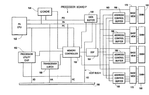
Referring now to Figure 4, the processor board P
is shown in more detail. The primary component on the
processor board P is the processor or CPU 152, in the
preferred embodiment preferably the P5 or Pentium
microprocessor from Intel Corp., the next generation
design after the 80486. In t~e preferred embodiment
the 66 MHz version is utilized. Operation and
lS interfacing of the 80386 and 80486 are assumed to be
familiar to the reader. The P5 is a very high
performance microprocessor having a superscalar
architecture and integrated and separate code and data
caches. The data bus is 64 bits wide and 8 parity bits
are provided. The data cache is a write-back design
having a 32 byte line width. Many of the signals of
the P5 have a similar function as in the 80386 and
80486 and only those signais have a changed or new
function will be described in detail herein. one
signal is CACHE, which is used to indicate whether the
cycle is cacheable by the processor 152. If this
signal is present during a read or write cycle, they
are burst cycles, namely cache line fill or write-back.
Further, the P5 has only a PBRDY* or processor bu~st
ready input and does not have a PRDY* or single cycle
ready input, so the PBRDY* input is used for all ready
indications to the processor 152. The P5 does include
a PNA* or next address input to allow address
pipelining.
21~Gl
one additional feature in the P5 is System
Management Mode or SMM as discussed at great length in
the background.
Three buses are connected to the P5 CPU 152, the
PD or processor data bus, the PA or processor address
bus and the PC or processor control bus. A level two
(L2) or external cache 154 is connected to the PD and
PA buses and receives control signals from a memory
controller 156. In the preferred embodiment the memory
controller 156 is a single ASIC which contains the
memory controller functions and additionally includes
the cache controller capabilities necessary to operate
the L2 cache 154.
A data buffer 158 is connected to the PD bus and
develops two new buses, the HD or host data bus and the
MD or memory data bus. The HD bus is connected to the
connector 100 for connection to the system board S.
The data buffer 158 is controlled by the memory
controller 156. A transceiver/latch unit 160 is
connected between the PA bus and the HA bus to provide
latching and transceiving capabilities of addresses
between the P5 CPU 152 and the host bus H. The
transceiver/latch 160 is controlled by the m~mory
controller 156 to allow posting of cycles from the
processor bus to the host bus H.
A processor utility chip 160 provides certain
necessary utility operations for use with the CPU 152.
The processor utility chip 162 is connected to the XD
bus and the HC bus and is controlled by the memory-
controller 156. The output of the processor utilitychip 162 is preferably provided to the PC bus to
provide control functions of the P5 CPU 152.
The memory controller 156 is also connected to a
unit referred to as the DDF or data destination
facility 164. The DDF 164 performs memory module
16 ~ t
enabling, address translation and memory segment or page
property storage. The DDF 164 provides memory capabilities to
indicate which particular bank of memory is to be enabled,
performs address translation on a 128 kbyte boundary and
provides indications of certain characteristics of each 128k
block, such as whether it is located in the main memory on the
processor board P or is external, write protected, high speed
and/or cacheable and whether that portion can be utilized by a
write-back cache. Operation of the DDF 164 is more completely
explained in Canadian Patent Application File No. 2,028,551 laid
open May 4, 1991 and EPO Application 0 426 386, publication date
May 8, 1991, both of which may be referred to for further
details. The outputs of the DDF 164 are a series of RASEN or
RAS enable signals for enabling a particular memory module,
certain translated addresses to indicate the address bits above
128k and the page characteristic bits, such as HNCA, HCW, HWP,
PLOCMEM* and SPD60.
The memory portion of the processor board P is provided as
four identical modules, each module containing an address/
control buffer 166, one sockets for receiving an individual SIMM
unit 168 and base memory 170. The address/control buffer 166
receives the PA bus, the address and enable outputs of the DDF
164 and control s,ignals from the memory controller 156. The
outputs of the address/control buffer 166 are the addresses
provided to the SIMMs 168 or base memory devices 170 and the
RAS*, CAS* and WE* signals. These signals are provided to each
of the SIMMs 168 and the base memory devices 170. Additionally,
each SIMM 168 or base memory device 170 is connected to the
memory data bus MD. As indicated, there are four like
modules. Other configurations of the processor board P
21 1.~ 4 ~ l
could be developed, with variations obvious to one
skilled in the art, with certain details provided
below.
Referring now to Figure 5, the various control
signals utilized by or provided by the memory
controller 156 are shown, with their appropriate
connections to the related bus or block. Figure 5 is
useful for an overview of the connections of the memory
controller 156 to the remaining components of the
computer system C.
Referring now to Figure 6, a block diagram of the
address/control buffer 166 is shown. The MSELCA* or
memory select column address signal is provided to a D-
type flip-flop 200. The clock of the flip-flop 200 is
provided by the PCLK signal, which is preferably the 66
MHz signal used as the clock by the processor lS2. The
non-inverted output of the flip-flop 200 is provided to
the select input of a 12 bit 2:1 multiplexor 202. The
MALE or memory address latch enable signal is provided
to the D input of a D-type flip-flop 204, the flip-flop
being clocked by the PCLK signal. The non-inverted
output of the flip-flop 204 is the SMALE signal and is
provided to the enable input of a ~1 bit latch 206.
The D inputs of the latch 206 receive the PAC16..4>
signals from the PA bus and the TA<25..17> translated
address signals from the DDF 164. The non-inverted
outputs of the portions of the latch 206 receiving
signals PA<16..13> and TA<24, 22..1,> are provided to
the one input of the multiplexor 202. The non-inYerted
outputs of the portions of the latch 206 receiving
signals PA<12..5> and TAc25,23> are provided as inputs
to the zero input of the multiplexor 202. The non-
inverted output of the latch 206 portion receiving the
PAc4> signal is provided to the address input of a
burst logic block 210. The burst logic block 210 is
211~4 ~ ~
used to increment, effectively invert, the address
being applied to the memories during burs~ operations,
that is, cache line fill and writeback operations, of
the processor 152. The burst logic 210 also receives
the MALE signal to indicate when to load an address and
the MADRINC* signal to increment the address when
active. Further, the PCLK signal is provided to the
burst logic 210 to perform the actual clocking
operation. The output of the burst logic 210 is the
least significant bit of the column addresses and is
provided to the zero input of the multiplexor 202. The
output of the multiplexor 202 is provided to the D
input of a 12 bit D-type flip-flop 212. The PCLK
signal clocks the flip-flop 212 and the Q or non-
inverted outputs are the MA<11..0> signals.
The REFRESH* signal is provided to the D input ofa latch 214 whose enable input receives the SMALE
signal. The output of the latch 214 is provided as one
input to a RAS decode logic block 216. The RASEN<l..0>
signals from the DDF 164, which indicate which bank of
memory is to be activated, either the base memory 170
or the SIMMs 168, are provided to the D inputs of a two
bit latch 218. The enable input to the latch 218 is
the SMALE signal. The output of the latch 218 is
provided as the other inputs to the RAS decode logic
216. The output of the RAS decode logic 216 is a two
bit signal which is active to indicate that either a
proper RAS has been selected or in the case of REFRESH
operation that both row addresses needed to be --
provided. The output of the RAS decode logic 216 isprovided to a two bit latch 220 whose enable input
receives the LMRAS* signal which is provided by the
non-inverted output of a D-type flip-flop 222. The
MRAS* signal is provided to the D input of the flip-
flop 222, which is clocked by the PCLK signal. In this
2~19~1
case the master RAS or MRAS* signal is thus used to
enable the decoded RAS signals. The non-inverted
outputs of the latch 220 are provided to one input of
two OR gates 224 and one input of two OR gates 226.
The second input to the OR gates 224 and 226 is
provided by the LMRAS* signal. The outputs of the OR
gates 224 are provided to the D inputs of a two bit D-
type flip-flop 228, which is clocked by the PCLK signal
and whose output are the RASA*<1..0> signals. The
outputs of the OR gates 226 are provided to the D
inputs of two bit D-type flip-flop 230, which is
clocked by the PCLK signal and whose outputs are the
RASB*<1..0> signals. The RASA* and RASB* signals are
used to provide additional fan out for the memory
driver system.
Four of the processor byte enable signals, that is
PBE*<3..0> or PBE<7..4> depending upon which
address/control buffer 166 is being referenced, each
address/control buffer 166 handling 32 bits of memory,
are provided to the D inputs of a 4 bit latch 232. The
enable signal for the latch 232 is the SMALE signal.
The outputs of the latch 232 are four inputs to CAS
decode logic 234. The PA<3> signal is provided to the
D input of a latch 236, which is enabled by SMALE
signal. The output of the latch 236 is provided to the
CAS decode logic 34. The MALLBES* memory or all byte
enables signal from the memory controller 156 is
provided to the D input Gf a latch 238, which is
enabled by the SMALE signal. The output of the latch
238 is provided to the CAS decode logic. The CAS
decode logic 234 has four outputs, namely the four
lines which are to activate the particular bytes of
memory to be provided by this address control buffer
166. The PA<3> signal is used to do selection between
the upper and lower 64 bits of the memory system and
2 ~ t
the PBE* signals are used for specific byte lane
encoding of these 64 bits. The four outputs of the CAS
decode logic 234 are provided to the D input of a 4 bit
latch 240. The enable signal to the latch 240 is the
LMCAS* or latched master CAS signal which is provided
by the non-inverted output of a D-type flip-flop 242.
The D input of the flip-flop 242 receives the master
CAS or MCAS* signal and is clocked by the PCLK signal.
The four outputs of the latch 240 are provided as
inputs to four two input OR gates 244 and as inputs to
four two input OR gates 246. The other inputs to the
OR gates 244 and 246 are provided by the LMCAS* signal.
The outputs of the OR gates 244 are provided to a 4 bit
D-type flip-flop 248 which is clocked by the PCLK
signal and whose non-inverted outputs are the
CASA*<3..0> signals. Similarly, the four outputs of
the OR gates 246 are provided to the D-type inputs of a
4 bit D-type flip-flop 250 which is clocked by the PCLK
signal and whose non-inverted outputs provide the
CASB<3..0>* signals. Again, duplicates are used to
provide additional fan out.
The MWE* signal is provided to the D input of a D-
type flip-flop 252, which is clocked by the PCLK
signal. The non-inverted output of the flip-flop 252
is provided to the D input of D-type flip-flops 254 and
256. The flip-flops 254 and 256 are clocked by the
PCLK signal and produce, respectively, the MWEA* and
MWEB* signals which are the memory write enable
signals. ---
Thus by properly providing the MRAS*, MCAS*, MALE,
MALLBES*, MADRINC* and WE* and MSELCA* signals to the
address/control buffer 166, the memory controller is
able to properly provide the RAS, CAS and write enable
signals in conjunction with the proper memory addresses
2~19~01
to allow page mode operation as well as interleaved
operation.
Figures 7, 8 and 9 disclose more details on
various portions of the data bufîer 158. Referring now
to Figure 7, the PD bus bits 63 to O and the parity
bits associated with these lines are provided to the
inputs of a 72 bit buffer 270. The outputs of the
buffer 270 are provided to the D inputs of four 72 bit
latches 272, 274, 276 and 278. These four latches
receive as enable inputs the LPDMDENO, LPDMDEN1,
LPDMDEN2 and LPDMDEN3 signals. The use of four latches
272-278 allows an entire burst from the processor 152
to be stored in a write posting operation. The outputs
of the latch 272 go to the zero input of a 3:1 72 bit
multiplexor 280. The outputs of the latch 276 go to
the one input of the multiplexor 280. The outputs of
the latch 274 go to the zero input of a second 72 bit
3:1 multiplexor 286. The outputs of the latch 278
similarly go to the one input of the multiplexor 286.
The select inputs to the multiplexors 280 and 286 are
connected to the LMDSEL<l..O~ signals. The outputs of
the multiplexors 280 and 286 are combined in parallel
to produce a 144 bit wide path which is provided to the
input of a 144 bit tri-state buffer 288. The output
control for the buffer 288 is inverted and is connected
to the LMDOE* signal. The output of buffer 288 is the
memory data bus, bits 127 to O of memory data and 16
bits of parity.
A 36 bit latch 290 and a second 36 bit latch-292
are connected in parallel to the output of the buffer
270. The enable inputs to the latches 290 and 292 are
provided by the LPDHDEN or latched processor data to
host data enable signal. The output of the latch 290
is provided to the zero input to a 32 bit 3:1
multiplexor 296. Parity data is not provided to
2 ~ 1 9 ~
multiplexor 296. The outputs of the latch 292 are
provided to the one input of the multiplexer 296. The
select input to the multiplexor 296 receives the
HDSEL<1..0> signals or host data select signals. The
outputs of the multiplexor 296 are provided to a 32 bit
tri-state buffer 298 whose inverted control input
receives the HDOE* signal. The output of the buffer
298 is connected to the 32 bits of the HD bus.
A channel is also necessary to go from the host
data bus to the memory data bus. To this end a 32 bit
buffer 300 is connected to the HD bus and has its
outputs connected to the D inputs of a 32 bit latch
302. The LMDHDEN or latched memory data-host data
enable signal is provided to the enable input of the
latch 302. The outputs of the latch 302 are provided
to a parity generator 304 which provides a 4 bit parity
output. The outputs of the latch 302 are also provided
to four 32 bit buffers 306, 308, 310 and 312.
Similarly, the outputs of the parity generator 304 are
provided to four 4 bit buffers 314, 316, 318 and 320.
The outputs of the buffers 306, 308, 314 and 316 are
paralleled to provide inputs to the third channel of
tne multiplexor 280 while the outputs of the buffers
310, 312, 318 and 320 are parallelled to provide the
inputs to the third channel of the multiplexor 286.
Thus, it is apparent that the same data from the host
data bus is provided four times across to the memory
data bus, but this is acceptable because the RAS decode
logic 216 and the CAS decode logic 234 in the add~ess
control buffer 166 actually control which data bytes
and which memory devices are actually active and
receive the data.
It is also necessary to get data from the host
data bus to the processor data bus. To this end the
output of the buffer 300 is provided to the D inputs of
211~
two 32 bit latches 322 and 324. The LHDPDENl signal is
the enable input to the latch 322 and the ~HDPDEN0
signal is the enable input to the latch 324. Parity
generators 326 and 328 are connected to the outputs of
the latches 322 and 324 respectively. The outputs of
the parity generator 326, the latch 322, the parity
generator 328, the latch 324 are provided to
appropriately sized buffers 330, 332, 334 and 336 so
that a 72 bit wide value of 64 data bits and 8 parity
bits is provided to the third input of a 72 bit 3:1
multiplexor 338. The selection control for the
multiplexor 338 is provided by the LPDSEL<1..0> or
latched processor data select signals. The output of
the multiplexor 338 is provided to the inputs of a 72
bit tri-state buffer 340 whose inverted tri-state
control receives the LPDOE* signal. The output of the
buffer 340 is connected to the 72 bits of the processor
data and parity bus. By use of the two latches 322 and
324, two complete accesses on the host data bus can be
combined in parallel to provide a 72 bit word which is
provided to the processor.
A path must also be provided from the memory data
bus to the processor data bus. To this end a 144 bit
wide buffer 342 is connected to receive the memory data
bus and the memory parity values. The outputs of the
buffer 342 are provided to 144 bit latch 344 whose
enable input receives the LMDPDEN signal. The outputs
of the latch 344 are provided to the zero and one
inputs of the multiplexor 338, with the lower 64 bits
and associated parity to the zero input and the upper
54 bits and associated parity to the zero input. In
this manner the multiplexor 338 can be used to select
between banks or interleaved portions of the memory
system.
2 1 ~
The data portions of the outputs of the buffer 342
are also provided in 32 bit segments to 4 inputs of a
4:1 32 bit multiplexor 350. The selection control for
the multiplexor 350 is provided by the MDHDSEL<1..0>
signal, which indicates which 32 bit portion of the
memory data is to be provided to the host data bus.
The output of the multiplexor 350 is provided to a 32
bit latch 352, whose enable input receives the LMDHDEN
- signal. The output of the latch 352 is connected to
the third input of the multiplexor 296.
As can be seen, the data buffer 158 contains the
necessary linkages and connections to allow data to be
transferred between any two of the buses in either
direction. Additionally, the buffer 158 contains
sufficient latching to allow an entire burst write
operation from the processor to be posted. Similarly,
the multiple operations from the host bus can be posted
or gathered until assembled for provision to the
processor system if necessary. Further, a write
operation from the processor to the host bus can be
posted.
Referring now to Pigure 8, the latching logic is
shown for the processor data to host or memory data bus
signals. The PDHDLE* signal is provided to a buffer
360, whose output provided to the D inputs of a latch
362 and of a D-type flip-flop 364. The PCLK signal is
provided to tne inverted enable input of the latch 362
and to the clock input of a flip-flop 364. The
inverted outputs of the latch 362 and flip-flop 364 are
provided as the two inputs to a two input AND gate 366,
whose output is the LPDHDEN signal. Similar
arrangements of buffers, latches, flip-flops and AND
gates are utilized with the PDMDLE*<3..0> signals to
produce the LPDMDEN<3..0> signals.
2 ~ /3'
Referring now to ~igure 9, the PDOE* signal is
provided to a buffer 368 whose output is provided to
the D input of a D-type flip-flop 370. The PCLK signal
clocks the flip-flop 370. The non-inverted output of
the flip-flop 370 is the LPDOE~ signal. Again, similar
buffer and flip-flop arrangements are used with the
PDSEL<1..0>, HDPDLE<1..0>, MDHDLE, MDPDLE, MDSEL<1..0>
and MDOE* signals to produce respectively, the
LPDSEL<l..0>, LHDPDEN<l..0>, LMDHDEN, LMDPDEN,
LMDSEL<1..0> and LMDOE* signals.
Referring now to Figure 10, portions of the memory
controller 156 are shown. Preferably the memory
controller 156 is organized as a series of
interdependent blocks. Each of these blocks is
logically organized to relate to a particular external
unit, such as the L2 cache 154, the processor 152, the
memory, the host bus H or arbitration, to which it is
related. A first block is referred to as FECON or the
front end controller 400. The FECON block 400
interacts with the prGcessor 152 for receipt of cycle
start signals from the processor 152 and provides
signals which activate the MCON block 402 and the HCON
block 404. Similarly, the FECON block 400 provides
completion signals to the processor 152 when
appropriate upon receipt of handshake signals from the
MCON block 402 and the HCON block 404. The FECON block
400 also provides signals to the data buffer 158 to
latch processor write data and enable processor read
data. The MCON block 402 is the second major blo~k and
is the memory controller portion. The MCON block 402
interfaces with the address/control buffers 166 to
provide the necessary control signals and the data
buffer 158 to latch aata from the memory and enable
àata to the memory. The HCON block 404 is the host bus
control block and interfaces with the host bus H to
L~
provide the necessary signals for its operation. The
HCON block 404 further communicates with the data
buffer 158 to latch data from the host bus H and enable
data to the host bus H. Both the MCON block 402 and
the HCON block 404 have handshake communications with
the FECON block 400 as will be more apparent in the
description below.
A CCON block 406 is the L2 cache controller and
interfaces with the FECON block 400 and the cache 154
to provide complete cache controller functions.
Preferably the cache controller is a 256 kbyte, direct
mapped, write through, lookaside cache for simplicity
of logic and operations. A block 408 referred to as
HARB or host arbitration block interfaces with the
FECON block 400 to provide processor and host bus
arbitration. The final block shown in Figure 10 is the
MPMON block 410 or memory performance monitor. In
memory controller 156 of the preferred embodiment the
memory performance monitor 410 is utilized to determine
the state of the MRAS* signal at the end of a memory
cycle. Effectively the MPMON block 410 is performing
next operation prediction so that the MRAS* signal can
be properly held low or raised high, dependi~g upon
whether the next operation has a probability of being a
memory page hit or memory page miss. More of this will
be described with the state machines described below.
Another block not shown in Figure 10 for
simplicity is the DDFCON or data destination facility
control block. This is omitted for simplicity b~t_
provides the necessary and conventional signals to
operate with the DDF 164 to allow it to be programmed
and read. This operation will be apparent based on the
previously referenced patent applications and the
operation of the FECON 400.
2 1 1 ~
Preferably the FECON block 400, MCON block 402 and
HCON block 404 are comprised of a plurality of state
machines, each acting independently and
interdependently, and certain loose logic. Each state
machine receives certain signals to commence its
operation and proceeds according to the receipt of
other signals. The various tasks necessary for the
memory controller operation are split between these
numerous state machines and between the control blocks
as indicated, to allow pipelining and multiple
concurrent cycles without re~uiring an overly complex
single master state machine. By the use of the
plurality of individual state machines each operation
is allowed to proceed at its greatest possible rate,
stopping only when another signal or information is
necessary to allow it to proceed. This arrangement and
operation will become apparent as the numerous state
machines are described below and by reference to
include timing diagrams. A number of these signals
provided and utilized internal to the memory controller
156 and between the various control blocks are shown in
Figure 10. The listing is not necessarily complete but
shows the more important signals. Further details of
the CCON or cache controller 406 will not be provided
2S as it is not particularly relevant to this operation
except as necessary when certain cache operations are
occurring.
Referring now to Figure 11, the FECON block 400
itself is made up of a series of sub-blocks or mo~ules.
The first block is the PCM or processor control module
410. This module 410 primarily receives the status
signals from the processor 152 and starts operation of
a cycle. A second block is the MCM or memory control
module 412, whicn interfaces more directly with the
MCON block 402. An HCM block 414 is used to interface
2 1 ~ 9 ~
28
with the HCON block 404. A block referred to as PNA or
processor next address generation 416 is utilized to
provide the next address or NA* signal to the processor
152 to allow full use of address pipelining. A block
418 referred to as PBRDYGEN or processor burst ready
generation is used to provide the ready signal to the
processor 152 to indicate that the data portion of a
cycle is completed and the next data portion can
proceed. The final block is the DPSELCM block 420
which is used to select the data path from the MD bus
or the HD bus to the PD bus.
Referring to Figure 12, the MCON block 402 is
shown with its constituent sub-blocks. A block 430 is
a CPUMEM block which effectively interfaces the
processor 152 with the memory itself. Included in the
CPUMEM block 430 is the processor memory state machine
which is utilized to develop the RAS and CAS and other
signals for processor cycles. Unless otherwise
indicated, all state machines advance on rising edges
of the PCLK or processor clock signal. A block 432
referred to as the ISABM or ISA bus master block is
used to interface with ISA bus masters and it contains
the memory state machine used wlth ISA bus masters.
Similarly, a block 434 referred to as EISABM or EISA
bus master provides the state machine and memory
control when an EISA bus master is in control and is
requesting memory operations. A block 436 referred t3
as the MABCON or memory address bus control block is
utilized to handle the memory addressing related --
signals. A MDBCON or memory data bus controller block
438 is used to handle the latch enable and output
enable signals of the data buffer 158 for memory and
host transfers. A block 440 referred to as SNPCON or
snoop control is used to indicate to the level 2 cache
154 and the processor 152 when snooping of a processor
21~ ~8~.
bus operation is appropriate to allow proper cache
coherency and write-back operation. The final block is
the REFSM or refresh state machine block 442 which
controls refresh operations to the memory devices.
Figure 13 is yet another similar block breakdown
for the HCON block 404. The HSYNC or host
synchronization sub-block 446 is used to track the host
bus H to determine cycle operations. The HOST or host
state machine block 448 is a host bus master used to
drive operations from the processor 152 to the host bus
H. A block 452 referred to as HACON or host address
control handles address related signals, while a block
454 referred to as HDCON or host data control controls
the data operations. It is understood that each of the
blocks 400, 402 and 404 include other miscellaneous
logic besides those sub-blocks shown.
Proceeding now to Figure 14, the first state
machine in the PCM block 410 is shown. As previously
noted, unless otherwise indicated, all of the state
machines described herein advance on rising edges of
the PCLK signal. This is the PPROG or processor cycle
in progress state machine and is used for basic cycle
tracking of the processor bus and provides two primary
signals, the PPROG or processor cycle in progress in
the memory controller 156 signal and the PEOC or
processor end of cycle signal. Variations on these
particular signals are provided for various modules.
On reset, the PPROG state machine starts at state A,
the idle state. The PPROG state machine proceeds-from
state A to state B when read operations, as indicated
by the state of the PWR or processor write/read signal
when a processor cycle is pending, as indicated by the
PPEND signal as it has been pipelined, or upon receipt
of the DSPADS or delayed synchronized processor ADS
signal. The SPADS signal is the ADS* signal from the
2119~1)1
_
processor 152 which has been synchronized to the PCLK
signal and inverted. The DSPADS signal is the SPADS
signal delayed one PCLK signal cycle. Under these
conditions control proceeds to state B. If the
processor 152 is not performing a burst cycle in state
B, the PEOC signal is provided during that state.
Control proceeds from state B to state C while burst
operations are occurring, as indicated by the PBURST
signal, and when the previous data cycle is completed,
as indicated by the PBRDY signal. Control proceeds
from state B to state F when a cycle is pending, it is
not a burst, the previous cycle has completed and the
cycle that is pending is a valid write cycle, that is,
it is not a memory code write. Control returns from
state B to state A if no further cycles are pending, if
a burst operation is not occurring and after the data
transfer has been completed as indicated by the PBRDY
signal, thus indicating an idle condition. In all
other cases, particularly when the PBRDY signal has not
been asserted, control remains at state B.
Control proceeds from state C to state D when the
PBRDY signal is asserted to indicate that a data
operation has been completed and otherwise remains in
state C. Control proceeds from state D to state E when
the next data operation has been completion as
indicated by the PBRDY signal. Otherwise control
remains at state D. There are three possible exits
from state E and a looping at state E. The PEOC signal
is asserted in state E. If the final data value of the
burst has been indicated as being transmitted, another
cycle is pending, and it is a read operation which is
pending, control proceeds from state E back to state B
and the next cycle proceeds. If the data value is
indicated as being provided and a cycle is not pending,
control returns to state A. If a cycle is pending, its
2 1 l9 ~ 0 1
a valid write cycle and the data transfer has been
completed, control proceeds to state F to begin a write
operation. In all other cases, particularly until the
data operation has been completed, control remains at
state E.
Control proceeds from state A to state F if a
valid write operation is indicated and a cycle is
pending or the DSPADS signal is active. Control
remains in state A during all cycles which are not
transfers to states B or F. In state F the PEOC signal
is asserted if a burst operation is not occurring. If
a burst operation is not occurring, the data transfer
has been completed as indicated by the PBRDY signal and
no cycle is pending, control proceeds from state F to
state A and idles until the next cycle. If the data
has been transferred as indicated by the PBRDY signal
and a burst operation is occurring, control proceeds to
state G. If a read cycle is pending, a burst is not
occurring and the data transfer has occurred, control
proceeds to state B. Otherwise control remains at
state F, particularly until data is ready. Control
proceeds from state G tO state H if the PBRDY signal is
provided and otherwise remains in state G. Control
proceeds from state H to state I upon receipt of the
PBRDY signal and otherwise remains at state H. In
state I the PEOC signal is asserted. Control proceeds
from state I to state A when the PBRDY signal is
asserted and otherwise remains in state I. In all
states other than state A the PPROG or processor ~ycle
in progress signal is asserted.
As indicated in discussing the PPROG state
machine, the signal referred to as PPEND or processor
cycle pending is necessary to allow full use of
pipelining. This signal is provided by the PPEND state
3s machine shown in Figure 15. This is a simple two state
21 I ~
state machine which is used to indicate that a
processor cycle has been requested while one is
currently in progress. Upon reset, the PPEND state
machine proceeds to state A, the idle state. Control
proceeds from state A to state B if the SPADS or
synchronized processor ADS signal is received and the
PPROG signal is true. In state B the PPEND signal is
asserted. Control proceeds from state B back to state
A upon receipt of the SEOC signal, which is a PCLK
synchronized version of the ANDing of the PBRDY signal
and PEOC signal, when the SPADS signal is not asserted.
Otherwise control remains in state B.
The PCM module 410 is also responsible for
developing the DPOE* signal. This is done in the DPOE
state machine as shown in Figure 16. Control initiates
at state A upon reset. Control proceeds to state D, a
wait state, if the memory system was currently
providing an output as indicated by the DSPADS signal
occurring during a read cycle which is not a memory
cache hit when a cycle is in progress (this being the
DPOE_OK signal definition) and the data transfer has
not completed as indicated by the PEOC and PBRDY
signals. Thus in this mode in state D the DPOE state
machine is waiting for the PD bus to become ready.
Control proceeds from state D to state B upon receipt
of the PEOC and PBRDY signals to indicate that the data
operation is completing, or from state A to state B if
this is a non-cache hit memory read cycle and a cycle
is not currently in progress or if it is a DPOE_OK--
condition, a cycle is in progress and the end of thatcycle is indicated by the PEOC and PBRDY signals. In
all other cases control remains at states A and D, as
appropriate.
Control proceeds from state B to state A if this
is other than a DPOE_OK cycle, an end of cycle has
2113~
occurred and upon receipt of a signal referred to as
EPBRDY or early processor bus ready, whic~ indicates
that in the next clock cycle the PBRDY signal will be
asserted. In this case the cycle is effectively
completed and the output control will be able to be
turned off because as indicated in the data buffer 158,
the DPOE signal which actually controls output is one
PCLK signal cycle delayed because of the internal
synchronizing flip-flop. Control proceeds from state B
to state C if it is proper to provide an output as
indicated by the DPOE_OK signal being active and the
cycle is not completed or an early ready has not been
received. In all other cases control remains at state
B. Control returns from state C to state B upon
receipt of the PEOC and PBRDY signals and otherwise
remains at state C. It is noted that when the next
state will be state B or state C or the state machine
is in state C, the DPOE* signal is active, that is
asserted low. Thus in this manner for non-cache hit
read cycles by the processor 152 the output enable is
active at the proper time. In general when referring
to signals in this description, an asterisk (*) after a
signal mnemonic indicates that it is logically true
when a low voltage level is present and is the inverse
of the signal mnemonic without an asterisk and angle
brackets with included numbers after a signal mnemonic
are used to indicate single or multiple bit positions
in a wider logical signal, such as the data or address
fields. Also for this description, state machine--
transition conditions are based on the level of theindicated signal, not its logical state.
Certain miscellaneous signals are also produced in
the PCM module 410. The first of these is the FEHLDA
or front end hold acknowledge signal. This is the
output of a D-type flip-flop clocked by the PCLK signal
2 1 1 ~
34
which has an input of the output of an AND gate which
receives as inputs signals indicating none of
processor, cache, memory, host bus read and host bus
write cycles are in process and a processor bus hold
request has been received. The second signal of
- interest is the PBURST signal which is provided by the
output of a D-type flip-flop clocked by the PCLK signal
and is provided at the beginning of cycles which are
processor cachable, such as cache line fills and write-
backs, or are L2 cache 154 read allocations, and is
removed at the end of the final one of the series of
such cycles.
Proceeding now to Figure 17, the first state
machine in the memory control module 412 is the MPROG
or memory in progress state machine. The state machine
begins at state A upon reset. There are four basic
paths out of state A, relating to single memory read
cycles, burst memory read cycles, single memory write
cycles and memory write-back or burst write cycles.
Control transfers from state A to state D, which is
used for single memory read cycles, when DSPADS signal
is active, a memory cycle is indicated by the MCYC
signal, a L2 cache line fill burst cycle is not in
progress as indicated by the FEBURST* signal and a read
is indicated. An L2 cache line fill operation is
always also a processor 152 cache line fill as a
processor 152 cache line fill miss is the cause of the
L2 cache 154 line fill. A processor 152 cache line
fill supplied by the L2 cache 154 is not an opera~ion
directed to the main memory and is treated as any other
cache hit. Control returns from state D to state A if
the SMRDY or synchronized memory ready signal is
provided and a cycle was not alread~- in progress on the
host bus prior to this memory cycle, as indicated by
the MPGHPG_lST signal, and neither a memory cycle is
211~4û1 -
pending nor is another memory cycle starting. The
MPGHPG lST signal is used to delay the return of data
so that concurrent read cycles to the host bus H and
memory do not get out of order. Control proceeds from
state D to state L if the memory is ready and a cache
cycle is in progress or if the SMRDY signal has been
received and a host bus cycle was started first.
Control proceeds from state D to state C if the memory
indicates ready, a host bus cycle was not already in
progress and either another memory cycle is pending or
another memory cycle is being initiated. Otherwise
control remains at state D.
Control proceeds from state L to state C if a host
cycle was not already in progress, a cache cycle is not
in progress and either another memory cycle is pending
or another memory cycle is commencing. Control
proceeds from state L to state A if an uncompleted host
cycle was not already in progress, a cache cycle is not
in progress and neither a memory cycle is pending nor
is another memory cycle commencing. In all other
cases, control remains at state L.
If a memory burst read is occurring, control
proceeds from state A to state E as indicated by the
DSPADS signal being true, a memory cycle being
indicated, a L2 cache line fill burst cycle being
indicated and a read cycle being indicated. Control
proceeds from state F to state E if either the memory
operation has indicated that it is ready and a cache
cycle is in progress or if the ready has previously
indicated and a host bus cycle was in progress first.
Otherwise, if the memory control has indicated that it
was ready as indicated by the SMRDY signal and a host
bus cycle was not already in progress, control proceeds
from state F to state G. Otherwise control remains at
state F. Control transfers from state E to state G
211~
when a signal referred to as MRDBHLD_LV or memory read
burst hold leave is active, indicating completion of
the burst. The development of the MRDBHLD_LV signal is
described below. Otherwise, control remains at state
E.
Control transfers from state G to state C if the
memory has indicated that it was ready and either a
memory cycle is pending or a memory cycle is being
indicated as commencing. Control transfers from state
G to state A if the memory has indicated its completion
and there is neither a memory cycle pending nor a
memory cycle commencing. In other cases, control
remains at state G pending the memory completion.
For single memory write cases, control transfers
from state A to state H based on the DSPADS signal,
MCYC and PWR signals being high and an indication that
this is not a processor cachable cycle. Control
proceeds from state H to state C when the memory
indicates that it is ready and either a memory cycle is
pending or is commencing. Control proceeds from state
H to state A if the memory indicates that it is ready
and there is neither another memory cycle pending nor a
cycle commencing. In all other cases control remains
at state H, generally awaiting completion of the memory
operation.
In the final case for exiting state A, control
proceeds from state A to state I for memory write-back
cycles. This is indicated by the DSPADS signal being
true, a memory cycle start is indicated by the MC~C
signal, the PCACHE or processor cachable signal is
present, and a write is occurring. Control proceeds
from state I to state J when the memory indicates that
it is ready. Otherwise control remains at state I.
Control proceeds from state J to state C if the memory
is ready and either another memory cycle is pending or
211~4~.
another memory cycle is commencing. Control proceeds
from state J to state A if the memory cycle is
completed as indicated and neither another memory cycle
is pending nor commencing. Two readys are necessary in
the preferred embodiment in this case as the processor
data cacAe line size is 256 bits or two memory
operations. Otherwise control remains at state ~.
Control proceeds from state C to state D if a
memory cycle is indicated by the MCYC signal, it is not
a burst and it is a read or if a signal referred to as
MRDPND or memory read pending is indicated as true.
The MRDPND signal development is described below.
Control proceeds from state C to state F for read burst
cases as indicated by a memory cycle indication, a
burst indication and a read or by the presence of the
signal MRDBPND for memory read burst pending. Control
proceeds from state C to state H on the indication of a
memory cycle, the fact that it is not processor
cacheable and that it is a write, that is a single
write cycle, or the MWRPND signal is active indicating
a memory write has been presented. In all other cases,
that is cache write-backs, control proceeds from state
C to state I.
The MPROG state machine produces several signals.
These signals are as follows:
MRD = MPROG STATE D
MRDHLD = MPROG STATE L
MRDBHLD = MPROG STATE E
MRDB1 = MPROG STATE F -_
MRDB2 = MPROG STATE G
MWR = MPROG STATE H
MWRB1 = MPROG STATE I
MWRB2 = MPROG STATE J
MPDREQ = (MPROG STATE E + MPROG STATE L)*
MPROG = (MPROG STATE A + MPROG STATE C)*
21194~
38
EMPROG = (MPROG STATE A + MPROG STATE C t MPROG
NEXT STATE A + MPROG NEXT STATE C)*
MEMRD = (MCYC & PWR*) + MRD + MRDBl + MRDB2 +
MRDHLD + MRDBHLD
MEMWR = MWR + MWRB1 + MWRB2
Thus it can be seen that the MPROG state machine
indicates when memory cycles are present in the memory
system by providing the MPROG, MEMRD, MEMWR and other
signals.
Referring now to Figure 18, the MPEND or memory
pending state machine is shown. As noted above, the
MPROG state machine utilizes as one of its branching
conditions the fact that a memory cycle is pending.
This signal is provided by the MPEND state machine.
Upon reset the MPEND state machine proceeds to the idle
state or state A. There are four exits from state A,
one for each of single memory read cycle, burst memory
read cycle, single memory write cycle and memory write-
back cycle cases. Control proceeds from state A to
state C when the DSPADS signal, the MCYC signals and
the MPROG or memory in progress signals are true and a
write is indicated and it not a processor cacheable
operation. Thus this is the single write case.
Control remains in state C while a memory cycle is in
progress as indicated by the MPROG state machine.
Otherwise control proceeds to state A.
Control proceeds from state A to state D for
memory write-back cycles as indicated by the DSPADS,
MCYC and MPROG signals being true and a write
indication and an indication that it is processor
cacheable. Control proceeds from state D to state A
when a memory cycle is not active and otherwise remains
in state D. Control proceeds from state A to state E
for memory cycles which are reads while a memory cycle
is in progress and which are not bursts. This is
2 ~ 4 ~ ~
indicated by the DSPADS, MCYC and MPROG signals being
true and a read being indicated in a non-burst case.
Control proceeds from state E to state A when the
memory cycle in progress has been completed and
otherwise remains at state E pending completion.
Control proceeds from state A to state F if the DSPADS,
MCYC and MPROG signals are true, indicating a memory
cycle is in progress and another one is requested, it
is a read cycle and bursting is indicated. Control
proceeds from state F to state A when the current
memory cycle in progress is completed. Otherwise
control remains at state F. The MPEND or memory cycle
pending signal is true when states C or D are to be
entered as the next state or when the state machine is
in states C, D, E or F. The MWRPND signal is true when
the next state is state C or the current state is state
C. The MWRBPND signal is true when the next state is
state D or the current state is state D. The MRDPND
signal is true during state E, while the MRDBPND signal
is true during state F.
The MCM module 412 is also responsible for
indicating when data is to be latched into the data
buffer 158 from the processor data bus on write cycles.
In the case of single write operations data is latched
into latches 272 and 274, while in burst operations all
four latches are utilized. However, it is noted that
in a single write case the DPMLE1 signal is actually
not generated as the decode later indicates that only a
single write is necessary. --
Upon reset of the system the MPMLE or processor to
memory latch enable state machine shown in Figure 19
starts at state A. The signals referred to as
SET_DPMLEO and SET_DPMLEl are active in state A when
the MWEPBRDY signal or memory write early PBRDY signal
is provided. Additionally, the DPMLE1 signal is
211~0~
provided in state D when the MWEPBRDY signal is active.
Control proceeds from state A to state C when the
MWEPBRDY signal is received from the MWEPBRDY state
machine (Fig. 21) indicating that this write cycle has
been posted and it is appropriate to proceed to the
next cycle. When the MWEPBRDY signal has not been
received, control remains at state A so that the first
two latches remain open. Control proceeds from state C
to state D if the MPROG state machine has indicated
that this is a burst write situation and the first
portion is proceeding as indicated by the MWRB1 signal.
Otherwise control proceeds from state C back to state
A. If the burst operation is occurring, the CLR DPMLE1
signal is asserted in state C so that the latch signal
is inactivated so that it can be made active again in
state D. Control remains in state D until the MWEPBRDY
signal is provided, indicating that the next of the
write cycles has been posted. Otherwise control
remains in state D. Additionally in state D the
SET_PMDRDY signal or set processor memory ready signal
is provided when the MWEPBRDY signal is indicated so
that a PMRDY signal can be provided to commence the
actual write cycle to the memory. Control proceeds
from state E to state F in all cases. State F is
utilized for the third write cycle in the burst
sequence and control remains at state F while the
MWEPBRDY signal is not being asserted, that is, to
indicate that this cycle has not been successfully
posted. When state F is active and the MWEPBRDY ~ignal
is asserted the SET_DPMLE2 signal is asserted so that
the latch 276 will be opened. Control proceeds from
state F to state G when the posting of the cycle has
been indicated. Control proceeds from state G to state
H after a single PCLK signal cycle. State H is the
final of the four write cycles in the write-back
' _ 211~? -
operation and control remains in state H until the
MWEPBRDY signal is asserted, at which time control
proceeds to state A. The SET_DPMLE3 signal is asserted
in state H when the MWEPBRDY signal is provided.
Additionally, the SET_PMDRDY signal is provided in
state H when the MWEPBRDY signal is provided to
indicate full width memory data can be provided to the
memory.
As indicated in the discussion of the MPMLE state
machine, the signal SET PMDRDY indicates that data has
been transferred into the posting buffers and can be
transferred. This signal is utilized by the PMDRDY
state machine shown in Figure 20. This state machine
commences operation in state A after reset. If the
SET_PMDRDY signal is received, control proceeds from
state A to state B. Otherwise control remains in state
A. From state B, control proceeds to state C if the
SET_PMDRDY signal is active and there is no indication
to clear PMRDY signal as being provided by the
CLR_PMRDY* signal. The CLR_PMRDY signal is the ANDing
of the MRDY signal and the OR of the MWR, MWRB1 and
MWRB21 signals. Thus, clearing the PMRDY signal is
appropriate if the memory has indicated that it is
ready and a write operation, either single or burst, is
indicated as being in progress. Control proceeds from
state B to state A if clearing of the PMDRDY signal is
appropriate and the SET_PMDRDY signal is not active.
Otherwise control remains in state B. Control proceeds
from state C to state B if it is appropriate to clear
the PMDRDY signal and its not set. Otherwise, control
remains in state C. The PMDRDY state machine thus
provides PMDRDY signal to indicate to the memory
control section that the write posting buffer has been
filled. The PMDRDY signal is active in states B and C
or when the MWR_PMDRDY signal is provided by the MPMLE
- 2 ~ J~
42
state machine, which is true when that state machine is
in state A, the MWEPBRDY signal has been received and
this is a single write operation. Thus the operation
commences in state A and proceeds to state B when the
first 128 bits is available and to state C if a second
128 bits is available and the first 128 bits has not
been actually written to the memory system. As each
128 bits is actually written the PMDRDY state machine
- backtracks from state C to state B to state A.
As noted above, the transitions in the MPMLE state
machine are based primarily on the presence of the
MWEPBRDY signal. This signal is provided by the
MWEPBRDY state machine shown in Figure 21. Upon reset
this state machine starts in state A, the conventional
idle state. Control proceeds from state A to state C
if the SPADS signal is active, a memory data write
cycle is decoded and either a processor cycle is not in
progress or a processor write cycle is completing or,
in a second alternative, if the DSPADS signal is
present, a main memory data write cycle is decoded and
a main memory data write cycle is in progress and
completing. Control proceeds from state A to state F
if the DSPADS signal is active, a local memory data
write cycle is decoded, a read cycle is in progress and
has not completed. Control proceeds from state A to
state G if the DSPADS signal is active, a main memory
data write cycle has been decoded and a memory read
cycle is completing, or if the DSPADS signal is active,
a memory data write cycle has been decoded and a ~ead
cycle is completing. Control proceeds from state F to
state G when the PPEOC signal is received and otherwise
remains in state F. Control always proceeds from state
G to state C. Control proceeds from state A to state H
if the DSPADS signal is active, a main memory data
write cycle has been decoded and a memory write cycle
21i3401
43
is active but not completing. In all other cases
control remains at state A. Control proceeds from
state H to state C when the PPEOC or end of cycle
signal is received and otherwise remains in state H.
Control proceeds from state C to state D if a main
memory data write cycle is decoded and otherwise
returns to state A. Control proceeds from state D to
state E if the first portion of a write-back is in
progress as indicated by the MWRB1 signal or if a
write-back is pending. Control proceeds from state D
to state A if a memory cycle is not in progress and a
memory write cycle is not pending or if a processor
cycle is not in progress. In all other cases control
proceeds from state D to state J. Control proceeds
from state E to state J if the PEOC signal is active,
indicating that the cycle is completing. In all other
cases control proceeds from state E to state I.
Control always proceeds from state I to state E.
There are numerous exits from state J. Control
proceeds from state J to state C if the SPADS signal is
active, a memory data write is decoded and a memory
cycle is not about to commence, a cache cycle is not
occurring, and a host bus cycle is not occurring and if
a processor read cycle is not occurring or, as a second
condition, if a single write cycle or a first portion
of a write-back cycle is occurring, a cache cycle is
not in progress and the currently in progress write
cycle is about to complete or, as a third condition, if
a memory write cycle or memory burst write cycle ~ 5
pending, a write cycle is in progress and no other
cycles are in progress. Control proceeds from state J
to state F if the DSPADS signal is active, a main
memory data write cycle is decoded, a memory cycle is
not in progress, the cycle is not completed to the
processor and either a cache cycle is in progress or a
21191~l
,_
host bus cycle is in progress. Control proceeds from
state J to state G if the DSPADS signal is true, a main
memory write data cycle has been decoded, a memory
cycle is not in progress and the current cycle is
completing. Control proceeds from state J to state A
if a memory cycle is not in progress, a memory write
cycle is not pending, a memory burst write cycle is not
pending and both the SPADS and DSPADS signals are not
asserted. In all other cases, control remains at state
J,
The MWEPRDY signal is asserted by this state
machine when the state machine is in state C, a main
memory data write cycle is decoded and the write cycle
is not to a write protected memory location as
indicated by the HWP signal being low or the SMIACT
signal being high. This is a first location where the
HWP signal is combined or qualified with the SMIACT
signal so that the HWP signal is overridden during
system management mode. In this case, if system
management mode was not entered and a write protected
location was being accessed, the MWEPBRDY signal would
not be produced because of the HWP signal term. But
the SMIACT signal is combined with the HWP signal and
overrides it, so that when system management mode is
active, the SMIACT signal term provides the necessary
indication for the MWEPBRDY signal to be produced as if
the memory location was not write protected. Further,
the MWEPBRDY signal is also active during state E.
The MWEPBRDY signal is considered an early rea~y
signal for local memory write operations and it will be
combined with other early ready signals and
resynchronized to actually provide the PBRDY signal.
As a result, it is provided one PCLK signal cycle
earlier then the PBRDY signal and so is considered
21~ 31
early. The assembly of these early ready signals is
described below.
The memory control module 412 is also responsible
for developing an early ready signal for main memory
read operations. This signal is provided by the
MREPBRDY state machine as shown in Figure 22. This
state machine begins operation on reset at state A.
Control proceeds from state A to state B if a host bus
cycle has not already started, a cache cycle is not in
progress and either the memory is ready and a single
memory read cycle has occurred or the memory is ready
and a memory read burst cycle is occurring or, as a
second alternative, if a memory early ready start
signal has been received. In all other cases control
remains at state A. The development of the MRERDY STRT
signal is shown in Fig. 38I.
The MRDHLD and MRDBHLD signals are provided to an
OR gate 820. The output of the OR gate 820 is combined
with the SHPROG_lST and HPROG* signals by AND gate 822.
The MRDHLD and MRDBHLD signals are also provided to an
OR gate 824. The output of the OR gate 824 and the
CPROG* and HPROG_lST* signals are combined by AND gate
826. An OR gate 828 receives the outputs of the AND
gates 822 and 826 and provides an output to the D input
of a D-type flip-flop 830, which is clocked by the PCLK
signal. The SHPROG-lST, MEMRD and SMRDY signals are
combined by an OR gate 832, whose output is combined
with the MRDHLD and MRDBHLD signals by OR gate 834.
The output of the OR gate 834 is combined with the_
CPROG* and HPROG-lST* signals in an AND gate 836. The
non-inverted output of the flip-flop 830 and the output
of the AND gate 836 are the inputs to an OR gate 838,
whose output is the MRERDY_STRT signal.
Control proceeds from state B to state C if this
is a memory read burst cycle or a memory read burst
2119~ ~1
46
cycle is being held for host or cache bus operations.
In all other cases control proceeds from state B to
state A. Control proceeds from state C to state D in
all cases and from state D to state E in all cases.
Control remains at state E until the MRDY or memory
ready signal is received from the memory controller
block 402 and at that time proceeds to state F.
Control then proceeds sequentially from state F to
state G to state H to state A on successive PCLX signal
cycles.
The MREPBRDY or memory read early PBRDY signal is
asserted in state B, D, F and H as appropriate for
single and burst operations. The MRDBHLD exiting
signal, referred to as MRDBHLD_LV, is provided in state
C to the MPROG state machine as previously described.
In addition, certain miscellaneous logic is
present in the memory control module 412. One of the
functions of this miscellaneous logic is to produce the
PDMDLE*<3..0> signals from the SET_DPMLE<3..0> signals.
The development of these signals is shown in Figure 23.
The MWR signal, asserted in state H of the MPROG state
machine, is an input to a two input OR gate 500 and a
two input OR gate 502. The MWRB1 signal or first
portion of a write-back cycle is provided to the second
input of the OR gate 500. The MWRB2 or second write-
back cycle portion signal, asserted in state J of the
MPROG state machine, is provided to the second input of
the OR gate 502 and indicates the second 128 bits of a
write-back cycle. The MRDY or memory ready signal,from
the memory controller block 402 is provided as one
input to two NAND gates 504 and 506. The second input
to the NAND gate 504 is the output of the OR gate 500,
while the second input to the NAND gate 506 is the
output of the OR gate 502. The output of the NAND gate
504 is one input to an AND gate 508, whose second input
211~01
is the inverted output of a D-type flip-flop 510. The
output of the AND gate 508 is provided to one input of
a two input OR gate 512, whose second input receives
the SET_DPMLE0 signal. The output of the OR gate 512
is provided to the D input of the flip-flop 510. The
inverted output of the flip-flop 512 is the PDMDLE*<0>
signal.
The output of the NAND gate 504 is also provided
to an inverted input of a two input NOR gate 514, whose
second input is not inverted and receives the
CLR_DPMLE1 signal. The output of the NOR gate 514 is
provided as one input to a two input AND gate 516,
whose second input receives the inverted output of a
D-type flip-flop 518. The output of the AND gate 516
is provided as one input to a two input OR gate 520,
whose second input receives the SET DPMLE1 signal. The
output of the OR gate 520 is provided to the D input of
the flip-flop 518. The inverted output of the flip-
flop 518 is the PDMDLE*<1> signal.
The output of the NAND gate 506 is provided as one
input to a two input AND gate 522, with the second
input to the AND gate 522 provided by the inverted
output of a D-type flip-flop 524. The output of the
AND gate 522 is provided as one input to an OR gate
526, whose second input is the SET_DPMLE2 signal. The
output of the OR gate 524 is provided to the D input of
the flip-flop 524. The inverted output of the flip-
flop 524 is the PDMDLE*<2> signal. The output of the
NAND gate 506 is also provided to one input of a 2-_
input AND gate 528, whose second input receives the
inverted output of a D-type flip-flop 530. The output
of the AND gate 528 is provided to one input of a two
input OR gate 532, whose second input receives the
SET_DPMLE3 signal. The output of the OR gate 532 is
provided to the D input of the flip-flop 530. The
2119~1
48
inverted output of the flip-flop 530 is the PDMDLE*<3>
signal. The PCLK signal is provided as the clocking
input to the flip-flops 510, 518, 524 and 530.
In a manner similar to the memory control module
412, the host control module 414 also includes a series
of state machines. The first of these is the HRD or
host read state machine shown in Figure 24. The state
machine tracks the read cycles, either single or burst,
that are running or executing on the host bus H. The
HRD state machine starts at state A upon reset.
Control proceeds from state A to state B when the
DSPADS signal is active, a host cycle read which is not
a burst is requested and either a host write cycle is
in progress or one is pending. Control proceeds from
state A to state F if the DSPADS signal is active, a
host read cycle is requested, it is a burst cycle and
either a host write cycle is in progress or one is
pending. Control proceeds from state A to state C for
requested host read, non-burst cycles when the DSPADS
signal is active and neither a host write cycle is in
progress nor is one pending. Control proceeds from
state A to state D on requests for host read, burst
cycles when the DSPADS signal is asserted and a host
write cycle is not in progress and one is not pending.
In all other cases control remains at state A.
Control proceeds from state B to state C if the
host ready signal has been provided or a host write is
not in progress and a host write is not pending. In
all other cases control remains at state B. Cont~Ql
proceeds from state F to state D if either a ready
signal is received from the host controller block 404
or a write cycle is not in progress, and a host write
cycle is not pending. In all other cases control
remains at state F.
2119~31
_
4g
Control proceeds from state C to state E if the
HREPBRDY or host read early PBRDY signal is asserted
and either a host read cycle is pending, a host read
burst cycle is pending, or the DSPADS signal is
asserted and a host read cycle is being asserted.
Control proceeds from state C to state A if the
HREPBRDY signal is asserted and it is none of the
further conditions mentioned for transfer to state E.
In all other cases control remains at state C. Control
proceeds from state E to state C if a host read is
pending and otherwise proceeds to state D. Control
proceeds from state D to state E if the HREPBRDY signal
is present, the PEOC signal is active and either a host
read is pending, a host burst read is pending or a host
read cycle has been sampled on the processor bus.
Control proceeds from state D to state A if the
HREPBRDY signal is present, the PEOC signal is present
and none of the additional conditions in the transfer
from state D to state E are present. In all other
cases control remains at state D. Host cycles are
identified as either I/O cycles or memory cycles where
the HLOCMEM* signal is high, indicating a non-main
memory location.
Two signals are provided by the HRD state machine.
These are the HRDPRG signal or host read in progress
signal, which is active during states B, C and D, and
the HOSTRD or host read signal, which is active during
states B, C or D and when a host cycle is active and
the processor is indicating a read request.
As noted, the HRD state machine utilizes as two of
its conditions the HRDPND and HRDPBND or host read
pending and host read burst pending signals. These are
provided by the HRDPND state machine of Figure 25. The
HRDPND state machine commences at state A at reset.
Control proceeds from state A to state B when the
211~01
_
DSPADS signal is asserted, a host read cycle is in
progress and a host non-burst read cycle is being
requested by the processor 152. Control proceeds from
state A to state C if the DSPADS signal is asserted, a
host read cycle is in progress and a host burst read
cycle is being requested by the processor 150 to the
host bus H. In all other cases control remains at
state A. Control proceeds from state B to state A when
the HRDPRG or host read in progress signal is
deasserted. In all other cases control remains at
state B. Control proceeds from state C to state A when
the HRDPRG signal is deasserted. In all other cases
control remains at state C. The HRDPND or host read
pending signal is asserted in state B, while the
HRDBPND signal is asserted in state C.
Just as the HRD state machine is used to track
host read cycles, similarly a state machine is used to
track host write cycles. This is the HWT state machine
as shown in Figure 26. The machine enters state A at
reset and proceeds from state A to state C if a host
write cycle is decoded, the previous cycle has been
acknowledged as indicated by the HACK signal being low,
write posting is enabled and a processor cycle is not
pending. Control proceeds from state A to state G if a
host write cycle is indicated, posting is not enabled
and a processor cycle is not pending, or if a write to
the host bus is requested, a processor cycle is pending
and ending and posting is not enabled. Control
proceeds from state A to state F if a host write ~cle
is requested, a processor cycle is pending and ending
and posting is enabled. Control proceeds from state A
to state E if a host write cycle is requested and a
processor cycle is pending and has not ended. In all
other cases control remains at state A.
21194~ ~
_
Control proceeds from state G to state C if a host
write cycle pending or if a host write cycle is
requested and posting is enabled, and in either case if
an SHRDY or synchronized HRDY signal is indicated, so
that the host bus is ready to receive the write
operation. The HRDY signal is provided at the non-
inverted output of a D-type flip-flop, which is clocked
by the PCLX signal. The output of a multiplexor is
connected to the D input, with the PHASE signal
providing the selection. The zero input receives the
non-inverted output of the flip-flop, while the one
input receives the HERDY signal, which is the inverted
version of the HERDY* signal present on the host bus H
to indicate a single cycle early ready indication.
Control proceeds from state E to state G if a processor
cycle is ending, as indicated by the PEOC and PBRDY of
SEOC signals and posting has been disabled. Control
proceeds from state E to state F when the processor
cycle is completing and posting is enabled. In all
other cases control remains at state E. Control
proceeds from state F to state C in all cases. Control
proceeds from state C to state D in all cases.
There are several exits from state D. ~he first
exit is from state D to state E, which occurs when a
ready is received, the host write cycle is being
requested or is pending, either a processor write cycle
is not in progress or the host write cycle was not
first, and if the processor cycle which is pending is
not completed. Control proceeds from state D to ~tate
F upon receipt of the SHRDY signal, either a write is
pending or a write is requested and posting is enabled,
and a read cycle which is in progress by the processor
is ending. Control proceeds from state D to state C
when ready is received and either another write cycle
is pending or is being requested and posting is
2 ~ a ~
enabled. Control proceeds from state D to state G if
the ready is received and a non-posted write cycle is
pending or a write cycle is pending and posting is
disabled. Control proceeds from state D to state A if
the ready is received, no write cycle is pending and no
- write cycle is being requested. The HWT state machine
also indicates when host write cycles are in progress
and when the ready signal is to be provided. The
HWTPRG or host write in progress signal is present,
when the HWT state machine is in other than state A.
The HWEPBRDY or host write early processor ready signal
is provided in state C or in state G when the HRDY or
host ready signal has been returned. The SET DPHLE
signal is active during state C.
As noted, the HWT state machine needs to know if a
write cycle is pending. This is done by the HWLlPND
state-machine of Figure 27. The state machine
commences at state A upon reset. Control proceeds from
state A to state B if a host write cycle is in
progress, a host write cycle is being requested,
posting is enabled and the previous write cycle has not
completed or if a second level of write cycle is posted
and pending. Control proceeds from state A to state C
when the DSPADS signal is true, a write cycle is in
progress, a write cycle is being requested, the write
cycle in progress has not completed and posting is
disabled or if a second non-posted write cycle is
pending. In all other cases control remains at state
A. Control proceeds from state B to state A when-a
ready is received from the host controller 404. In all
other cases control remains at state B. Control
proceeds from state C to state A when a ready is
returned and otherwise remains at state C. The
HWTLlPND or first level host write pending signal is
active during state B, while the HWTNPLlPND or host
211~01
53
first level not posted write cycle pending is true in
state C.
As just mentioned, it is possible to have three
host bus write cycles pending at one time. This is
possible because one cycle can be posted to the host
bus H, one cycle can be posted to the EISA bus E from
the host bus H and another one can be pending from the
processor 152. Therefore it is necessary to track to
two levels. This tracking is done by the HWL2PND state
machine of Figure 28. This state machine commences at
state A upon reset and proceeds to state B when the
DSPADS signal is active, a write cycle to the host bus
is being requested and posting is enabled and either a
first write cycle, either posted or not posted, is
pending. Control proceeds from state A to state C if
the DSPADS signal is active, a host write cycle is
being requested, posting of that cycle is not enabled
and a cycle is already pending. In all other cases,
control remains at state A. Control proceeds from
state B to state A when a posted or non-posted write
cycle is not pending. That is, the previously pending
cycle is no longer pending but has completed. In other
cases control remains at state B. Similarly, control
proceeds from state C to state A if the prior pending
signal has been performed. Control remains at state C
otherwise. The HWTL2PND or nost write posted level 2
pending signal is active in state B, while the
HWTNPL2PND or level 2 write pending non-posted signal
is active in state C.
Just as a processor ready signal is provided in
write cases, it is also necessary to provide an early
processor ready in read cases. This is done by the
HREPBRDY state machine of Figure 29. This state
machine commences at state A upon reset. Control
proceeds to state B if a host read is in progress, a
2119~
54
host write is not in progress, a processor cycle is
pending, the current processor cycle is not ending and
the host bus cycle which is in progress was not
commenced prior to the processor cycle which is in
progress. In all other cases control remains at state
A. Control proceeds from state B to state C if the
current processor cycle is completing and the host bus
cycle has not completed. Control proceeds from state B
to state D if the host bus cycle is completing and the
processor cycle is not completing. Control proceeds
from state B to state E if both the host and processor
cycles are completing. Control otherwise remains at
state B. Control proceeds from state C to state A when
the host cycle is completing. Otherwise control
remains at state C. Control proceeds from state D to
state E when the processor cycle is completing.
Otherwise control remains at state D. Control always
proceeds from state E to state A.
The HREPBRDY or host read early PBRDY signal is
provided in state E, in state C if the host bus cycle
is being completed or in state A if a host write cycle
is not in progress, the host cycle that was in progress
was first and it is being completed.
Certain miscellaneous logic also contained in the
host control module 414 is shown in Figure 51. The
PDHDLE* signal is provided as the inverted output of a
D-type flip-flop 700. The PDHDLE* signal is also
connected to an OR gate 702. The OR gate 702 receives
the SET_DPHLE signal from the HWT state machine as_its
other input. The output of the OR gate 702 is ANDed
with an indication of the inverted HRDY signal in NAND
gate 704. The output of the NAND gate 704 is provided
to the D input of the flip-flop 700. The flip-flop 700
is clocked by the PCLK signal. The logic also develops
the HPROG or host bus cycle in progress signal. This
2119.,~
is developed as the output of an OR gate 706. The OR
gate 706 receives the output of an OR gate 708 and the
noninverted output of a D-type flip-flop 710. The OR
gate 708 receives the HRDPRG host read in progress
signal, the HWTPRG host write in progress signal and
the HWLlPEND host write pending signals. The output of
the OR gate 706 is one input to an AND gate 712, with
the second input receiving the output of a NOR gate 714
which in turn receives the PEOC and PBRDY signals to
indicate that the current processor cycle is not
completing. The output of the AND gate 712 is provided
as the D input of the flip-flop 710. The flip-flop 710
is checked by the PCLK signal. The final signal of
interest produced by the HCM module 414 is the ignore
parity check or IGNPCHK signal. This signal is
utilized by the processor 152 during read operations
from the host bus H because parity is not maintained on
the host bus H. The IGNPCHK signal is provided as the
noninverted output of a flip-flop 716 whose input
receives the output of a two input OR gate 718. One
input to the OR gate 718 is provided by the noninverted
output of a D-type flip-flop 720. The second input is
provided by the noninverted output of a D-type flip-
flop 722, which is also connected to the D input of the
flip-flop 720. The HREPBRDY signal is provided to the
D input of the flip-flop 722 and all three flip-flops
716, 720 and 722 are clocked by the PCLK signal.
Upon reviewing the data buffer 158 it is seen that
the FECON module 400 must also provide the PDSEL<1_.0
signals-to allow proper control of the multiplexor 338
during read cases. This is done primarily by the use
of the DPSEL state machine shown in Figure 30. This
state machine commences at reset in state A and
proceeds to state C if a host read cycle is in progress
(as indicated by the HRD state machine being in states
2 1 1 9 ~
B, C or D or if a host read cycle is occurring) and
will be returning its data first because the host cycle
was started first as indicated by the HPROG_lst signal.
Control proceeds from state A to state B under several
different conditions. The first of those is if a
memory read cycle is in progress, the early PBRDY
signal has been provided, the cycle has not completed
and there is not a host read cycle in progress which
was in progress first. A second condition for a
transfer from state A to state B is if a memory read
cycle is occurring, the early PBRDY is provided, the
cycle is ending and the cycle which is being completed
had the PA<3> bit cleared, as indicated by the LPAI03
signal. The final condition of transfer from state A
to state B is if a memory read cycle is occurring as
indicated by the MEMRD and MCYC signals, the memory
cycle has been acknowledged by the memory controller
block 402, the PA<3> signal was cleared to indicate the
lower 64 bits and the PBRDY signal has not been
asserted. In all other cases control remains at state
A.
Control proceeds from state B to state C if a host
read cycle which was started first is occurring.
Control proceeds from state B to state A for the same
conditions which were true for transfers from state A
to state B except that the PA<3> bit would be set as
utilized in those particular conditions. Otherwise
control remains at state B. Control proceeds from
state C to state A when a host read cycle is not -
occurring, a memory read cycle is occurring and bitPA<3> is not set. Control proceeds from state C to
state B if a host read cycle is not occurring, a memory
read cycle is occurring and the PA<3> bit is set.
Otherwise control remains at state C.
21I94~1
The particular state of the DPSEL state machine
determines the selection of the multiplexor. In state
A the signals referred to as NPDSEL<1..0> are set to
indicate the first channel. In state B the
NDPSEL<1..0> signals are set to indicate the second
channel, while in state C the NDPSEL<1..0> signais are
set to indicate the third input of the multiplexor 338.
The NDPSEL<1..0> signals are provided to the inputs of
two D-type flip-flops, with the PDSEL<1..0> signals
produced by the non-inverting outputs of the flip-flop,
with the flip-flops being clocked by the PCLK signal.
One signal which must be provided to the processor
152 to allow pipelining is a signal referred to as PNA
or processor next address. The processor 152 sees this
signal and knows that it can provide the next address
in a pipelined mode. Therefore it is necessary to
properly generate the PNA signal. A series of state
machines and random logic are utilized to provide this
signal. The first state machine is the PNA state
machine of Figure 31. This state machine is used to
provide an indication that a PNA signal can be provided
within a given window. The state machine begins at
state A upon reset. Control proceeds from state A to
state B if the SPADS signal is true and a signal
referred to as EPNA_DEC or early PNA decode is
provided. The EPNA DEC signal is developed under two
conditions. The first is a processor read cycle which
is not to a local, i.e. processor bus, location and is
not a special cycle. The second is that a non-special,
non-local processor write cycle which is not being
responded to by the L2 cache 154 and is not a code
write is being requested. Otherwise control remains at
state A. Control proceeds from state B back to state A
if the PPEOC signal is asserted, indicating that the
cycle is completing. Control proceeds from state B to
2 1 ~
-
state C if the PNA signal is asserted and the cycle is
not completed. Control remains at state B in all other
cases. Control proceeds from state C back to state A
if the SPADS signal is asserted and the EPNA_DEC signal
is not asserted or if the cycle is ending. Control
proceeds from state C back to state B if the SPADS
signal is asserted, the current cycle is ending and the
EPNA_DECWR signal or write condition noted above is not
true or a read is not in progress. Control proceeds
from state C to state E if the SPADS signal is active,
the current cycle is not completing and the EPNA_DEC
signal is active. Control proceeds from state C to
state D if the SPADS signal is active, the cycle
currently in progress is completing and the EPNA_DEC
signal is asserted. In all other cases control remains
at state C. Being in state D is an indication that the
operation is pipelined. Control proceeds from state D
to state B if the PPEOC signal is asserted, indicating
that a cycle is completing. Otherwise control remains
at state D. Control proceeds from state E to state B
in all cases.
The PNA state machine provides one signal and this
is the PNA_OK signal when the state machine is in state
B. This is an indication that it is possible to
receive another address as one cycle is not currently
pipelined or is effectively completing.
A state machine referred to as the RDPNA state
machine is shown in Figure 32 and is used to indicate
that the PNA signal can be generated for the current
read cycle. Control commences at state A upon reset.
Control proceeds from state A to state B if the signal
EPNA_DECRD, the read term of the EPNA_DEC signal, is
true and any of the following sets of conditions is
true. First, if a MCYC or memory cycle is indicated
and an acknowledgement has been received from the
211~
59
memory control block 402. Second, if a host cycle is
active and an acknowledgement has been received from
the host control block 404. Third, if the DSPADS
signal is active and the cycle is neither a memory
cycle or a host cycle. In all other cases control
remains at state A. Control proceeds from state B back
to state A if the PNA signal is asserted or if the
current cycle is completing as indicated by the PPEOC
signal. Otherwise control remains in state B. The
RDPNA_OK signal is generated in state B or when the
next state is going to be state B.
A similar state machine, the WRPNA state machine,
is shown in Figure 33 and is used to generate the
WRPNA_OK signal for write cycle cases. This state
machine begins at state A on reset and proceeds to
state B under one of three conditions. The first is
that the SPADS signal is asserted, the EPNA_DECWR
signal is asserted, a memory write is not occurring and
either a host write is not in progress or the host
control block 402 has acknowledged an operation. The
second condition is if the SPADS signal and the
EPNA_DEC signals are both asserted, a memory write
cycle is in progress and has been acknowledged as
completing soon by the EMACK signal and either a host
bus write is not in progress or it has been
acknowledged. The final condition is if a host cycle
is occurring, it is has been acknowledged, it is a host
write which is in progress, a PNA signal has not been
sent and the EPNA DECWR signal has been asserted.- ~n
all other cases control remains at state A. Control
returns from state B to state A if the PNA signal has
been asserted or if the cycle has ended as indicated by
the PPEOC signal. Otherwise control remains at state
B. The WRPNA_OK signal is developed if the state
machine is in state B or if the next state is state B.
2~19~01
The PNAGEN module 416 includes some random logic
to generate the actual PNA signal. The PNA signal is
generated by the non-inverting output of a flip-flop,
with the PNA* signal generated by the inverted output
of the flip-flop. The flip-flop is clocked by the PCLX
signal. The input to the flip-flop is provided by the
output of an OR gate which has inputs of the PNA OK
signal, the HPNA_OK signal and the output of an OR gate
which combines the RDPNA_OK and WRPNA_OK signals. The
HPNA_OK signal is the output of a NAND gate which has
as its inputs a signal indicating that host write cycle
is in progress and the output of an OR gate, which has
as one of its inputs a signal indicating that a host
read cycle is in progress and as its second input an
AND gate which has as its inputs a signal which
indicates that a host cycle is present and the
EPNA_DECRD signal.
As indicated above, numerous of the state machines
use the PBRDY or processor burst ready signal to
advance. Certain special cycles such as branch trace
messages as provided by the processor 152 must not be
provided to the host bus H to prevent errors, but ready
indication must be provided. Additionally, the
processor 152 must receive ready indication for write
operations to write-protected areas, even though no
actual operation will occur. The EPBRDY signal for
these particular cases is provided by the WPEPBRDY
state machine shown in Figure 34. The state machine
begins at state A upon reset and transfers to state B
if the DSPADS signal is true, a data write to local or
main memory is indicated, SMI mode is not active and
write protect status is indicated from the DDF 164 or
if the DSPADS signal is true and a branch trace message
has been decoded, with the additional condition in both
cases that a processor cycle is not in progress in the
2113~
memory controller 156 or that a cycle which is in
progress is ending and the PBRDY signal is asserted.
Control proceeds from state A to state C if the DSPADS
signal is asserted, a local memory write data operation
is indicated, SMI mode is not active and the write
protect indication is received from the DDF 164 or if
the DSPADS signal is true and a branch trace message
has been decoded, both of these combined with the fact
that a processor cycle is in progress. Otherwise
control remains at state A. Control always proceeds
from state B to state A. Control proceeds from state C
to state B when the cycle in progress is completed as
indicated by the PEOC and PBRDY signals being asserted.
Otherwise control remains at state C. The WPEPBRDY
signal is asserted in state B. Thus this state machine
is used to provide the processor BRDY indications in
the case of writes to write protected memory or on
branch trace messages. In the case of the writes to
write protected areas none of the other state machines
perform this operation and the data is actually
ignored. Similarly, the data is ignored for branch
trace messages and they are not passed to the host bus
H.
It is noted that the WPEPBRDY state machine does
not provide the WPEPBRDY signal if SMI mode is active,
as indicated by the SMIACT signal, and an operation is
directed to an otherwise write protected location. The
WPEPBRDY state machine simply stays at state A, with
the MWEPBRDY state machine handling the early rea~y
signal generation is this case which is treated as a
normal write case.
With the development of this final EPBRDY signal,
it is appropriate to describe the logic which develops
the PBRDY signal. The signal referred to as EPBRDY
signal is developed by ORing together the MREPBRDY,
2 1 1 ~
62
MWEPRDY, HREPBRDY, HWEPBRDY and WPEPBRDY signals. This
signal is ANDed with an indication that the cache
controller is not performing a cache line fill and
provided to the input of a D-type flip-flop. The
noninverted output of the flip-flop is the PBRDY
- signal, while the inverted output of the flip-flop is
the P8RDY* signal which is provided to the processor
152.
As previously noted, two signals referred to as
MCYC and HCYC have been utilized. As indicated in
Figure 10 the MCYC signal is provided to MCON block 402
and HCYC signal is provided the HCON block 404 to
indicate that they have cycles to perform. This
decoding is done by certain logic.
The MCYC logic is shown in Figure 35. A six input
AND gate 550 receives the PMIO, PDC, PWR*, PLOCAL*,
CHIT_OK* and HLOCMEM signals to decode a main memory
data read cycle which is not ax L2 cache 154 hit. A
six input AND gate 55Z receives the PMIO, PDC*, PWR*,
PLOCAL*, HLOCMEM and CHIT_OK* signals to decode a
memory command read cycle which is not a L2 cache 154
hit. A six input AND gate 554 receives the PMIO, PDC,
PWR, PLOCAL* and HLOCMEM signals and the output of a
two input OR gate 556 which receives the SMIACT and
HWP* signals. Thus this AND gate 554 decodes a memory
data write cycle. It is noted that the SMIACT and HWP*
signals are ORed in the OR gate 556. This is the final
location where the two signals are combined and is done
so that areas of memory which are normally write --
protected, such as the SMRAM, are not write protectedduring system management mode. In normal write protect
cases the MCYC signal would never get generated, so
that a memory cycle would never get run and the
WPEPBRDY state machine would handle the cycle. But
when the SMIACT signal is present, the HWP signal
2II~Gl-
63
indication is overridden and a full write cycle is
performed. Thus an area of conventional memory can be
utilized as the SMRAM without danger of if being
overwritten and yet it is fully accessible during
system management mode.
The outputs of the AND gates 550, 552, 554 are
provided to the inputs of a three input OR gate 557
whose output is provided as one input to a two input
AND gate 558. The second input of the AND gate 558
receives the DSPADS signal. The output of the AND gate
558 is provided as one input to a two input OR 560,
whose second input receives the noninverted output of a
D-type flip-flop 562. The output of the OR gate 560 is
the MCYC signal and is provided to the input of a two
input AND gate 564. The second input of the AND gate
564 is inverted and receives the MACK signal. The
output of the AND gate 564 is provided to the D input
of the flip-flop 562, which flip-flop 562 is clocked by
the PCLK signal.
The development of the HCYC signal is shown in
Figure 36. A four input AND gate 570 receives the
CHIT_OK*, PMIO, PDC, and PWR signals to decode a host
bus memory data write operation. A five input AND gate
572 receives the PMIO, PDC*, PWR*, HLOCMEM* and
CHIT OK* signals to decode a host bus memory command
read operation which is not a cache hit. A five input
AND gate 574 receives the PMIO, PDC, PWR*, HLOCMEM* and
CHIT_OK* signals to decode a host bus memory data read
operation which is not a cache hit. A 2 input OR-gate
576 receives the PMIO* and PWR* signals to decode host
bus I/O read operations. A three input OR gate 578
receives the PMIO*, PDC and PWR signals to indicate a
host bus I/O data write operation. The outputs of the
AND gates 570, 572 and 574 and the OR gates 576 and 578
are provided as inputs to a seven input OR gate 580.
~Il9~
64
The PLOCAL and HSPCYC signals, wnich indicate
respectively processor bus local cycles and special
cycles which are to be transmitted to the host bus,
that is 80486 equivalent special cycles, provide the
remaining inputs to the OR gate 580. The output of the
OR gate 580 is provided as one input to a two input AND
gate 582, whose second input receives the DSPADS
signal. The output of the AND gate 582 is provided as
one input to a two input OR gate 584. The second input
to the OR gate is connected to the non-inverting output
of a D-type flip-flop 586. The flip-flop 586 is
clocked by the PCLK signal. The output of the OR gate
584 is provided as one input to a two input AND gate
588, whose second input is inverted and receives the
output of a two input AND gate 590. The output of the
AND gate 588 is provided to the D input of the flip-
flop 586. The HACK signal is provided as one input to
the AND gate 590 and the output of a two input NAND
gate 592 provides the second input. The PPROGRD and
PWR signals are the inputs to the NAND gate 592. The
output of the NAND gate 592 is also provided as one
input to a 2 input AND gate 594, whose second input
receives the output of the OR gate 584. The output of
the AND gate 594 is the HCYC signal. This completes
the description of the front end controller 400.
The memory control block 402 is shown in more
detail in Figure 12 and its state machines will be
discussed at this time. The CPUMEM module 430 is
responsible for the actual control of memory operations
directed from the processor 152. The core of the
CPUMEM module 430 is the MEM or memory state machine as
shown in Figure 37. Control proceeds to state MI or
memory idle upon reset. In this state the state
machine is idle and is precharging the DRAMs and the
MRAS* signal is high. Control proceeds from state MI
2119401
to state MRC if the MCYC signal is active, indicating
that a memory cycle is being requested, and the CHGTO*
or not charge ~ime out signal is asserted, indicating
that the DRAMs have not been fully precharged. Control
proceeds from state MI to state MR1 or memory RASl if a
cycle has been requested, as indicated by the MCYC
signal, and the CHGTO signal is true, indicating that
the precharge time has completed. Control proceeds
from state MI to state MN when the BMPROG or bus master
cycle in progress signal is asserted. In all other
cases control remains at state MI. Control proceeds
from state MRC to state MRl when the CHGTO signal is
active, indicating that the precharge time has been
completed. Control proceeds from state MR1 to state
MR2 in all cases. Control proceeds from state MR2 to
state MCl, the first of the CAS states, if the DRAMs
have a speed of 60 ns, as indicated by the LSPD60 or
latched SPD60 signal from the DDF 164, and either a
read cycle has been indicated or the PMDRDY or
processor to memory data ready signal is active.
Control proceeds from state MR2 to state MR4 for 60 ns
DRAMs if a write cycle has been requested and the
PMDRDY signal is not asserted. In all other cases
control proceeds from state MR2 to MR3. Particularly,
control proceeds from state MR2 to MR3 in the case of
80 ns DRAMs. Control proceeds from state MR3 to state
MR4 in all cases. Control proceeds from MR4 to state
MCl if either a read cycle has been requested or the
data is available as indicated by the PMDRDY signal.
Control remains at state MR4 for all other cases.
Control always proceeds from state MCl to state
MC2. Control proceeds from state MC2 to state MC3 when
the MPDREQ signal is asserted, indicating that the
FECON block 400 is ready to accept data from the
memory. In all other cases control remains at state
2119q Ql
MC2. Control always proceeds from state MC3 to state
MN.
There are numerous exits from state MN. In state
MN the MRAS* signal is low. Control proceeds from
state MN to state MCl if a burst cycle is occurring, if
- a non-burst memory page hit read has occurred as
indicated by the MCYC, BURST*, MWR* and PGHIT signals
being true or if the next cycle is a non-burst memory
page hit, the previous cycle was a memory write, and
the data is available, as indicated by the MCYC signal,
BURST*, PGHIT, PMDRDY and PRMWR signals being asserted.
The PRMWR signal indicates the previous memory cycle is
a write cycle. This loop from state MN to state MC1 is
the shortest loop and indicates a two wait state loop
based on a 66 MHz clock. Thus, once page hits are
obtained, the memory controller 156 can operate in two
wait state per memory cycle mode for most page hit
operations. Control proceeds from state MN to state
MR4 on non-burst memory page hit writes where the data
is not available, as indicated by the MCYC, BURST*,
MWR, PGHIT and PMDRDY* signals being true. Control
also proceeds from state MN to state MR4 if it is a
non-burst, memory page hit with a write following a
read operation, as indicated by the MCYC, BURST*, MWR,
PGHIT and PRMWR* signals being true. Control proceeds
from state MN to state MRC if another cycle has been
requested and it is a non-burst, non-page hit, as
indicated by the MCYC, BURST* and PHGHIT* signals being
true. Control proceeds from state MN to state MI-lf an
idle state is needed for non-burst, non-bus master
cycles, non-memory cycles either because the memory
performance monitor has indicated that the next cycle
probably will not be a page hit and therefore it is
appropriate to proceed to precharge the DRAMs to see if
time can be saved in the case of a page miss, or if a
2 1 1 ~
hold request has been acknowledged by the processor
152. These conditions are indicated by the MCYC*, the
BURST* signal, and the BMPROG* signals being true and
either the HHLDA or MPM HIT*. In all other cases
control remains at state MN, which is thus effectively
a second idle state, only in this case the MRAS* signal
is held low. Particularly, if the memory performance
monitor indicated that the next state is likely to be a
page hit, control remains at state MN, awaiting the hit
and a transfer to states MCl or MR4.
As noted, the MEM state machine needs to know
whether a burst is occurring. This information is
provided by the BURST state machine shown in Figure 38.
This state machine beings operation at state A upon
reset and proceeds to state B if a cache burst
operation is occurring and a new cycle is being
developed, based on the NEWCYC and CBURST signals. The
NEWCYC signal is the AND of the MACK and MCYC signals,
while the CBURST signal indicates a processor 152
write-back or L2 cache 154 send allocate line fill. In
all other cases control remains at state A. Control
proceeds from state B to state C when the MBRDY signal
is received to indicate that 128 bits of data had been
transferred to the memory system. Otherwise control
remains at state B. Control proceeds from state C back
to state A on the next occurrence of the MBRDY signal
and otherwise remains at state C. Thus, once the
beginning of a new burst cycle is indicated, control
proceeds from state B to state C as data is -_
transferred. The BURST signal is thus asserted during
states B and C, while the BURST2 signal is asserted in
state C and the EBURST signal is provided in state B.
The CHGTO or precharge timeout signal is provided
by a simple counter. The counter is loaded with a
default value of 4 whenever the MRAS signal is being
211.~01
68
asserted. Assertion of this signal is described below.
On each rising edge of the PCLK signal when the MRAS
signal is deasserted, that is the MRAS* signal is high,
the counter counts down. When tne counter reaches a
value of 1, this is an indication that the precharge
time has been completed for 60 ns DRAMs. When the
counter counts down to 0, this is an indication that
the precharge time has completed to 80 ns DRAMs.
Therefore the CHGTO signal is provided after three
counts for 60 ns DRAMs and four counts for 80 ns DRAMs
from the beginning of the MRAS* signal deassertion.
The PGHIT or page hit signal is provided by a page
hit detection block. This is relatively conventional
block in that it contains a latch for processor address
<27..12> bits, with the latch operating on the
processor memory address latch enable signal, which is
active when addresses are being provided to the
memories. The outputs of the latch are provided to one
input of a comparator, while the active or current
processor address <27..12> bits are provided to the
second input of the comparator. If they are equal,
this is considered to be a page hit operation, so that
a new row address need not be provided.
Certain miscellaneous logic is also contained in
the CPUMEM module 430. The first function is the
generation of the MRDY signal (Fig. 38A). The MRDY
signal is provided as the output of a D-type flip-flop
740 clocked by the PCLK signal. The D input to the
flip-flop 740 receives the output signal of a
multiplexor 742, with the select input receiving the
MWR signal. The zero input of the multiplexor 742 is
connected to the output of an AND gate 744 which
receives the EBURST* signal and a signal indicating
that the next state of the MEM state machine is state
MC2. The output of the AND gate 744 is also provided
2119~
69
to the D input of a D-type flip-flop 746, which is
clocked by the PCLK signal and whose output is the
LMRDY or EMACK signal. The one input of the
multiplexor 742 receives a signal indicating that the
next state is MC3. This same signal is provided to the
D input of a D-type flip-flop 74~, which is clocked by
the PCLK signal and whose output is the MBRDY signal.
The MACK or memory acknowledge signal is developed
as shown in Figure 38B. A signal indicating that the
next state is state MN and the EBURST* signal are
provided to the input of an AND gate 750. The output
of the AND gate 750 is one input to an OR gate 752
whose other input is a signal indicating that the next
state is state MI. The output of the OR gate is the
NMACK signal is provided to the D input of a flip-flop
754. The flip-flop 754 is clocked by the PCLK signal
and has the MACK signal as its noninverted output.
The MRASSC or master RAS set signal from the CPU
section is the same as the signal indicating that the
next state is state MR1. The MRASRC or master RAS
reset from the CPU signal is shown as the output of a
three input OR gate 756 in Figure 38C. The next state
MC3, MCYC, PGHIT*, and BURST2 signals are provided to
an AND gate 758. The BURST*, PGHIT*, MCYC, and next
state MN signals were provided to an AND gate 760. The
outputs of the AND gate 758 and 760 are provided as
inputs to the OR gate 756, along with a signal that
indicates that the next state of the MEM state machine
is state MI. The NMCASC or next cycle master CAS-_
signal from the CPU section is equivalent to a signal
indicating that the next state is state MC.
The NMALEC or next cycle memory address/enable
signal from the CPU is provided as the output of an OR
gate 762 as shown in Figure 38D. The next state MC3
and EBURST* signals required as the inputs to an AND
21 19 ~ 0~
gate 764. The next state MN, EBURST*, and MCYC*
signals are provided as the input to an AND gate 766.
The outputs of the AND gate 764 and 766 and a signal
indicating that the next state is MI are the inputs to
the OR gate 762.
The NMADRINCC or next cycle memory address
increment signal from the CPU section is equivalent to
the next state being state MC3 during a BURST
operation. The MALLBESC or memory all byte enables
signal from the CPU section is provided during read
cycles or during cache BURST operations. The NMWEC or
next cycle memory write enable signal from the CPU
section is provided as the output of an OR gate 768 as
shown in Figure 38E. The next state any MR or any MC
signal and the MWR signals are the inputs to an AND
gate 770. The next state NM, NXTCYC, PWR! PRMWR, and
EBURST* signals are the inputs to an AND gate 772. The
next state MN, MWR, and E8URST signals are the inpu~s
to an AND gate 774. The outputs of the AND gate 770,
772, and 774 are the inputs to the OR gate 768.
The NDMPLE or next cycle memory data to processor
data latch enable signal is equivalent to the next
state of the state machine being MC 3 during read
operations. The NDMSELOC or next cycle memory data
select a least significant ~it from the processor
section signal is provided as the output of an OR gate
776 as shown in Figure 38F. The next state MC3 and
next state MN signals are provided as inputs to an OR
gate 778, whose output is provided to an AND gate-~80,
whose other input receives the EBURST signal. The next
state MC1 and next state MC2 signals are the inputs to
an OR gate 782 whose output is an input to an AND gate
784, whose other input receives the BURST2 signal. The
outputs of the AND gates 780 and 784 are the inputs to
the OR gate 776.
211~40~
-
The NMDOEC or next cycle memory data output enable
signal from the CPU section signal is provided by the
output of a NOR gate 786. The next state any MR or any
MC state signal and the indication that the machine is
in state MC3 are provided as the inputs to an OR gate
778. The output the OR gate 778 is provided as an
input to an AND gate 790, whose other input receives
the MWR* signal. The next state NM, EBURST, and MWR*
signals are the inputs to an AND gate 792. The next
state MN, NXTCYC, PWR*, and EBURST* signals are the
inputs to an AND gate 794. The outputs of the AND
gates 797, 792, and 794 and the RDHLD signal are inputs
to the NOR gate 786. The RDHLD signal is provided as
the noninverted output of D-type flip-flop 796 which is
clocked by the PCLK signal. The state MC3, PRMWR* and
EBURST* signals are provided to an AND gate 798, whose
output is connected to the D input of the flip-flop
796.
The IMALE signal is a one PCLK delayed version of
the MACK signal. The signal is used to latch the PWR
signal to develop the MWR signal, to latch the PDC
signal to develop the MDC signal and to latch the SPD60
or memory speed 60 signal to develop the LSPD60 signal.
The PMALE or processor memory address latch signal
used with the page hit detector is developed when the
HHLDA signal is low, the MACK signal is true, the MCYC
signal is true. The NXTCYC signal is produced as the
output of an OR gate 800 as shown in Figure 38H. The
SPADS and PMIO signals are provided as the inputs-to an
AND gate 802, whose output is one input to the OR gate
800, with the MCYC signal being the other input to the
OR gate 800.
There are also additional types of bus masters
which could operate in the computer system C. One of
these is an ISA or Industry Standard Architecture bus
2lls4nl
master which would be located in the EISA slots 108.
As these bus masters can add_ess main memory, it is
appropriate to have a control module, ISABM 432, and a
state machine for use with their operation. The state
machine is tAe ISA state machine of Figure 39. The
state machine starts at state II upon reset. ~his is
the ISA idle state. When an ISA command is not active,
control remains at state II. When an ISA command is
active, with the definition of the signal defined
below, control proceeds from state II to state IR2.
Control proceeds from state IR2 to state IR3 on the
next PCLX signal clock edge and then from state IR3 to
state IR4. If a snoop write-back is occurring, that is
the write-back cache in the processor 152 has
determined that a read hit has occurred and a write-
back is appropriate, control remains at state IR4 until
this operation is completed. When the snoop write-back
is completed, control proceeds from state IR4 to state
IC1. Then, on successive positive edges of the PCLK
signal, control proceeds from state IC1 to state IC2 to
state IC3 and then to state IL. Control remains in
state IL as long as the ISACMD signal is activated.
Control proceeds from state IL to state II when the ISA
command has been completed.
The development of the ISACMD signal is shown in
Figure 40. The MRDC and MWTC signals are provided as
two inputs to an OR gate 600. The output of the OR
gate is one input to a four input AND gate 602. The
other inputs to the AND gate 602 are the HHLDA, -_
REFRESH* and EMSTR16 signals. Thus the output of the
AND gate 602 is active when an ISA bus master has
control of the EISA bus E and is actively running a
cycle. The output of the AND gate 602 is the XISACMD
signal and is provided to the D input of a D-type flip-
flop 604. The inverted clock input of the flip-flop
2119~1
604 receives the HCLK or host bus clock signal, which
is developed by dividing the PCLK signal by two for a
66 MHz PCLK signal. The output of the AND gate 602 is
also provided to D input of a D-type flip-flop 606,
whose positive clock input receives the HCLK signal
from the host bus H. The noninverted outputs of the
flip-flops 604 and 606 are the zero and one inputs,
respectively, of a 2:1 multiplexor 608. The select
input to the multiplexor 608 is provided by the PHASE
signal, which indicates that the PCLK signal is in
phase with the HCLR signal, that is, the two rising
edges are aligned. The PHASE signal is the noninverted
output of a D-type flip-flop which is clocked by the
PCLK signal and receives the HCLK* signal at its D
input. The output of the multiplexor 608 is provided
to the D input of a D-type flip-flop 610 whose clocking
input receives the PCLK signal. The noninverted output
of the flip-flop 610 is the ISACMD signal.
As with memory state machine, the ISA state
machine also provides the signals for controlling the
address/control buffer chips 168 and the data buffer
158. The MRASSI or master RAS set ISA signal is active
when the ISA state machine is in state II, the ISACMD
signal is true and the cycle is being addressed to the
main memory. The MRASRI or master RAS reset by ISA
signal is asserted in state IL when the ISACMD signal
is not asserted. The NMCASI or next cycle master CAS
by ISA signal is asserted when any of the next states
is state IC1, IC2 and IC3, when the operation is to
main memory and the operation is not to write protected
memory or is a read operation. The NMWEI or next state
MWE from the ISA portion signal is asserted when the
next state will be IR4 or one of the IC1, IC2 or IC3
states, an ISA write operation is being re~uested and
it is not to write protected space. The MALLBESI or
21~9~
74
memory all byte enables by ISA signal is asserted
during read cycles when the ISACMD signal is asserted.
The NDMHLEI or next memory data to host data latch
enable signal from the ISA system signal is provided
during writes in state IR2 or during reads in state
IC2. The DHOEI or host data output enable by ISA
signal is provided during ISA read operations when the
ISACMD signal is asserted. The NMDOEI signal is
negated when for read operations the next state will be
the IR4, IC1, IC2 or IC3 states, the current state is
state IC3, or the RDHLD signal is asserted.
The ISABM logic 432 is also responsible for
providing the CHRDY signal. The logic for this is
shown in Figure 41. The SNPWB signal is provided to
the D input of a D-type flip-flop 620. The PCLK signal
clocks the flip-flop 620. The synchronous clear input
receives the output of a two input OR gate 622 which
receives as its inputs signals indicating that the ISA
state machine is in state II or state IC3. The
noninverted output of the flip-flop 620 is provided as
one input to a three input AND gate 624, whose other
two inputs receive the indication that the state
machine is in state IC2 and that a read operation is
occurring. The output of the AND gate 624 is provided
to the load input to a 7 to 0 down counter 626. The
PCLK signal clocks the counter 626. The output of the
counter 626 is a zero signal, which is referred to as
the CHRDYTO or CHRDY time out signal. This signal is
provided as one input to a two input AND gate 62B7_with
the other input receiving an indication that the state
machine is in state IL. The XISACMD signal and the
HCW* or not write-back signal are provided as the
inputs to a two input AND gate 630. The XISACMD*
signal and an indication of state II are provided as
the inputs to a two input AND gate 632. A two input
2119~0~
AND gate 634 receives the output of an OR gate 636 and
the output of a NAND gate 638. The inputs to the NAND
gate 638 are the ISARD signal, indicating a read
operation by an ISA bus master, and the output of the
flip-flop 620. The inputs to the OR gate 636 are
indications that the ISA state machine is in state ICl,
IC2 or IC3. The outputs of the AND gates 628, 630, 632
and 634 are provided as the inputs to an OR gate 640,
whose output is the CHRDY signal.
Just as an ISA bus master has a separate control
module 432, an EISABM module 434 is provided and it
includes a state machine referred to as the EISA state
machine which is shown in Figure 42. The state machine
begins operation after reset at state EI or EISA idle.
It remains in this state until the EISA START or ESTRT
signal is received. The ESTRT signal is true when the
START, SBCLK, HMIO, REFRESH*, EMSR16* and HHLDA signals
are true and the PCLK signal is in phase with the HCLK
signal. At that time it proceeds to state ERS.
Control remains at state ERS until the PCLK
synchronized BCLK or SBCLK signal is not asserted.
Control then proceeds to state ERW. Control remains in
this state while the SBCLR signal is not asserted.
Control proceeds from state ERW to state EW1 in the
case of the SBCLK signal being asserted and a write
operation occurring. Control remains in state EW1 when
both the SBCLK signal and BCLK signals are not
asserted, as indicated by the SBCLKHI signal. When
they are both asserted, control proceeds from sta~e EW1
to state EW2. Control proceeds to state EC1 to EW2 in
all cases on the next PCLK signal cycle. Control
proceeds directly from state ERW to state EC1 when the
SBCLK signal is true and a read operation is occurring.
Control proceeds from state ECl to state EC2 on~5 the next rising edge of the PCLK signal. Control
2~19~1
76
proceeds from state EC2 to state EC3 during read
operations and then to state EST on the next PCLK
signal edge. Control proceeds directly from state EC2
to state EST for write operations. If a snoop write-
back is occurring, control proceeds from state EST tostate EWB, where it remains during the write-back
operation. When the write-back is completed, control
proceeds from state EWB to state EC1 to reexecute the
operation which was interrupted by the write-back. If
a snoop write-back is not occurring and both the SBCLK
and BCLK signals are low, as indicated by the SBCLKLO
signal, or if a snoop write-back is not occurring and a
write has occurred, control proceeds from state EST to
state EN. In all other cases control remains at state
EST. Control proceeds from state EN to state ENW if
the synchronized EXRDY or SBEXRDY signal is not
asserted. The SBEXRDY signal is the EXRDY signal first
synchronized to the falling edge of the BCLK signal and
then synchronized to the PCLK signal in phase with the
HCLK signal. Control remains in state ENW when either
of the SBCLK and BCLK signals are asserted and moves to
state EN on the SBCLKLO signal. Control proceeds from
state EN to state ERW if an EISA burst is occurring and
the operation is ready, as indicated by the SMSBURST
and SBEXRDY signals. The SMSBURST signal is the
MSBURST signal synchronized to the PCLK signal when
both the BCLX and HCLK signals are low. If a burst is
not occurring and the cycle is completed, as indicated
by the SBEXRDY signal being high, control proceeds_from
state EN to state EI to enter idle state.
Just as the ISA and CPUMEM modules 432 and 430 had
to develop the various signals for controlling the
address/control buffers 166 and the data buffer 158, so
does the EISA module 434. One signal which is produced
is the HSTRETCH* signal, which is provided to the EISA
211~
bus controller 110 to extend the BCLK signal to provide
certain incremental timing without having to take a
full BCLK wait state. The logic for developing the
HSTRETCH* signal is shown in Figure 43. A D-type flip-
flop 650 is clocked by the PCLK signal and has itsinput tied to the non-inverting output. The state ERW
and RESET signals are inputs to a two input OR gate
652, whose output is provided to the synchronous clear
input of the flip-flop 650. The state EWB indication
is provided to the synchronous set input of the flip-
flop 650.
The noninverted output of the flip-flop 650 is
also provided to one input of a two input AND gate 654,
whose second input receives the EC or state EC1, 2 or 3
indication. The output of the AND gate 654 is provided
to the D input of a D-type flip-flop 656. The output
of a two input AND gate 658, which receives the PHASE
and PCLK signals, is provided to the clock input of the
flip-flop 656. The noninverted output of the flip-flop
656 is provided to one input of a three input OR gate
660, whose other two inputs receive a signal indicating
that the next state will be state EC1, EC2 or EC3 or a
signal indicating that the current state is state EC1,
EC2 or EC3. The output of the OR gate 660 is provided
as one input to a three input AND gate 662. The HWR*
and LOCMEM signals are the remaining inputs to the AND
gate 662 to indicate a main memory read. A two input
AND gate 664 receives the SNPWB and EI* or EISA state
machine not in state EI signals. The output of the AND
gate 664 and the output of the AND gate 662 are the two
inputs to an OR gate 666, whose output is provided to
the D input of a D-type flip-flop 668. The PHASE and
PCLK signals are provided to an AND gate 670, whose
output clocks the flip-flop 668. The noninverted
output of the flip-flop 668 and the output of the AND
78
gate 664 are provided as the two inputs to a NOR gate
672, whose output is the HSTRETCH* signal.
The MRASSE or master RAS set by EISA portion
signal is provided either when the next state will be
state ERW or the MRASSR signal is being provided. The
MRASSR signal is the set signal based on the refresh
state machine being in state RB. The refresh state
machine will be described below. The MRASRE or master
RAS reset by EISA signal is provided when either the
next state is state EI and the current state is state
EN, indicating a transfer to idle, or the MRASSR signal
is asserted. The MRASRR signal indicates that the
refresh state machine is in state RC and the SBCLKLO
signal is asserted. The NMCASR or next cycle master
CAS refresh signal is asserted when the refresh state
machine is in states RA or RB. The NMCASE or next,
master CAS by EISA cycle signal is asserted either when
the NMCASR signal is asserted or when the next state is
state EC, a main memory operation occurring and it is
either not write protected or is a read operation. The
NMWEE or next cycle memory write enable by EISA signal
is provided when the next state is either EW2, EC, or
EWB, and a not write protected write to main memory is
occurring. The NMALEE signal is provided when the next
state is other than states ECl, EC2 or EC3. The
MALLBESE signal is provided during read operations when
the state is other than EI or ERS or when the refresh
state machine is not in state RI. The NDMHLEE or next
cycle MDHD latch enable by EISA signal is provide~
during state EWl for reads and state EC2 for writes.
The NDHOEE or next cycle HD output enable by EISA
signal is provided during the ERW states which are
reads to local memory and is provided to the input of a
latch which has its open or enable period on the high
level of the CMD* signal. The output of the latch is
21~ 9~01
79
the DHOEE signal. The NMDOEE or next cycle MD output
enable by EISA signal is not asserted when read
operations are occurring and the next state is state
ERW, EC1, EC2, EC3, or EBW, the state is state EC1,
EC2, or EC3 or the state following an EC1, EC2 or EC3
state, i.e. the first entry into state EST.
The REFRESH state machine used in the REFSM module
442 is shown in Figure 44. It commences operation
after reset in state RI, where it remains until it sees
the RSTRT or refresh start signal. The RSTRT signal is
provided when the SBCLK signal, the START signal, the
REFRESH signal and the HHLDA signal are asserted. This
is the indication of the beginning of the start portion
of a refresh cycle on the EISA bus. When the RSTRT
signal is asserted, control proceeds from state RI to
state RW. Control proceeds to state RA and then to
state RB on successive PCLK signal rising edges.
Control remains at state RB until the SBCLKHI signal is
asserted. At that time it proceeds to state RC and
then to state RI.
The MABCON module 436 provides the various MRAS*,
MCAS*, MALLBES*, MALE, MWE*, MSELCA*, and MADRINC*
signals to the address/control buffers 166. The MRAS
or master RAS signal and MRAS* signal are provided at
the outputs of a JK flip-flop which receives at its J
input the OR of the MRASSC, MRASSI and MRASSE signals
and at its K input receives the OR of the MRASRC,
MRASRI and MRASRE signals. This flip-flop is clocked
by the PCLK signal. The MCAS* signal is provided-as
the inverted output of a D-type flip-flop clocked by
the PCLK signal and receiving at its D input the OR of
the NMCASC, NMCASI and NMCASE signals. The NMSELCA
signal is produced by the AND of the MRAS signal, the
SPD60 signal and a signal indicating bus master cycle
is not in progress. This signal is provided to the D
2119~Ql
_
input of a flip-flop which is clocked by the output of
an AND gate which receives the MRAS and PCLK signals.
The inverted output is the MSELCA* signal. The
MALLBES* signal is provided as the output of a
multiplexor which receives as its select input the
signal indicating that a write-back is not occurring
and has as its zero input the output of a NOR gate
which receives the MALLBESE and MALLBESI signals and as
its one input the inverse of the MALLBESC signal. The
MALE signal is provided at the output of a D-type flip-
flop whose input receives the AND of the NMALEC and
NMALEE signals and is clocked by the PCLK signal. The
MADRINC* signal is produced at the noninverted output
of a D-type flip-flop which receives the NMADRINCC*
signal and is clocked by the PCLK signal. The MWE*
signal is produced by the inverted output of a D-type
flip-flop which receives at its D input the OR of the
NMWEI and NMWEE signals and is clocked by the PCLK
signal when no write-back is in progress.
The MDBCON module 438 provides the various
selects, latches and output enable signals to the data
buffer 158 by combining them from various other
sources. The MDSEL<1..0> signals are provided by the
output of two D-type flip-flops whose inputs receive
the NDMSEL<1..0> signals and are clocked by the PCLK
signal. The NDMSEL<l> signal receives a signal
indicating that a write-back is not in progress, while
the NDMSEL<0> signal receives the output of an AND gate
which receives at its inputs the NDMSELOC signal ~nd
the BMNOWB* signal. The MDHDLE signal is provided at
the non-inverting output of a D-type flip-flop clocked
by the PCLK signal whose D input receives the output of
an OR gate which receives the NDMHLEI and NDMHLEE
signals. The MDPDLE signal is provided at the output
of a PCLK signal clocked D-type flip-flop which
21t9~1
81
receives at its input the NDMPLE signal. The MDOE*
signal is provided as the inverted output of a D-type
flip-flop which receives at its D input the AND of the
NMDOEI and NMDOEE signals and is clocked by an AND gate
whose inputs are the synchronized BMNOWB and PCLK
signals. The HDOE* signal is provided at the output of
a NOR gate which receives the DHOEI and DHOEE signals.
One other function in the MCON module 402 is the
SNPCON or snoop control module 440. This module 440 is
responsible for providing snoop strobes to be used by
the various caches and to provide an indication that a
write-back is occurring. This module 440 utilizes the
snoop state machine shown in Figure 45. This state
machine commences at state SI upon reset. When the
PEADS or processor external address signal is not
received, control remains at state SI. The PEADS
signal is provided at the output of a D-type flip-flop
which is clocked by the PCLK signal and receives at its
D input the output of an AND gate which receives the
HNCA* signal to indicate a cacheable address and the OR
of the SNPSTBI and SNPSNBE signals. The SNPSTBE signal
is produced during state ERW when the SBCLK signal is
asserted. The SNPSTBI signal is asserted when the
NISACMD signal is true and the ISACMD signal is not
true. When it is received, control proceeds to state
SW1 and then to states SW2 and SW3 on succeeding PCLK
signal rising edges. If there is no indication that a
processor cache hit has occurred, control returns to
state SI. If a hit has occurred, control proceeds_to
state SWB1. Control remains at state SWB1 until the
SPADS signal is received. Control then proceeds to
state SWB2. Control remains in this state until the
LMRDY signal is received, at which time control
proceeds to state SWB3 and from there to state SI. The
SNPWB or snoop write-back in progress signal is
211~
82
provided when the state machine is in states SWBl, SWB2
or SWB3.
Various other miscellaneous signals are produced
in the MCON module 402. For example, the BMPROG or bus
master in progress signal is produced by the ORing of
- the BMPROGI and BMPROGE signals. The BMPROGI signal is
the ISACMD signal, while the BMPROGE signal is provided
when the EISA state machine is not in state EC or the
refresh state machine is not in state R1. The BMNOWB
or bus master in progress and not writing back signal
is produced by the ANDing of the BMPROG bus master in
progress and SWBPROG* or synchronized write-back in
progress signals. The SWBPROG signal is provided when
the snoop state machine is in state SWBl or the next
state is state SWB2.
The MDHDSEL<1..0> signals are produced by the
HA<3. 2> signals, which are produced as follows. The
NHALEI and NHALEE signals are ANDED to form the NHALEBM
signal. The NHALEE signal is active when the next
state of the EISA state machine will be state EI, ENW
or EN, the state is EI or ERS or if the state is EC2, a
write is occurring and it is not a snoop write-back.
The NHALEI signal is the inverse of the ISACMD signal.
The NHALEBM signal in turn is used as the selection
input for multiplexors connected to the D inputs of two
D-type flip-flops, which are clocked by the PCLK
signal. The one input of the multiplexors receives the
HA<3> and HA<4> signals from the HA bus as being driven
by the bus master. The zero input of the multiplexors
receives the non-inverted output of the flip-flops.
The non-inverted outputs of the flip-flops is also
provided to the inputs of two latches. The OR of the
BMLEI and BMLEE signals is provided as the enable input
for the latches. The BMLEI signal is asserted when the
ISA state machine is in state IR2. The BMLEE signal is
211~
asserted when the EISA state machine is in state ERW.
The non-inverted outputs of the latches are the
BM_HA<3..2~ signals, which are also the MDHDSEL<1..0>
signals.
The HCON module 404 also includes a number of
state machines and modules to develop it necessary
signals. The first of these modules is the HSYNC or
host sync module 446. The HSYNC state machine is shown
in Figure 46. Control proceeds on reset to state HSI,
where control remains while the HCYC signal from the
FECON module 400 is not received. As soon as the HCYC
signal is received, control proceeds to state HSH,
where it remains until the NHSTRT or next cycle host
start signal is true or when phase is not properly
asserted, that is, the PCLK and HCLK signals are do not
have their rising edges aligned. If the NHSTRT signal
is not asserted and the phase is proper, control
proceeds to state HSP. Control remains in state HSP
while the NHSTRT signal is not asserted. If the NHSTRT
signal is asserted at the same time as the HCYC signal,
indicating another cycle is requested, control returns
to state HSH. If the NHSTRT signal is asserted and the
HCYC signal is not asserted, control returns to state
HSI to idle.
The NHACK or next cycle HACK signal is provided
during transfers when the next state will be state HSI
or when the current state is state HSP and the NHSTRT
signal is asserted. The HACK signal is provided at the
output of a D-type flip-flop clocked by the PCLK signal
and receiving the NHACK signal at its D input. The
HREQ or host cycle requested signal is asserted when
the next state is the HSH state, during the HSH state
or when the HATO signal is not asserted. The HATO
signal indicates that the necessary address cycles have
been completed.
2119~1
84
The next control module utilized in the HCON
module 404 is the HOST module 448, which uses the HOST
state machine shown in Figure 47. This module 448
provides the control of signals on the host bus when
the memory controller 156 is acting as a bus master.
Control commences at state HTI upon reset and remains
in that state while the HREQ signal is not asserted,
indicating that a host bus cycle has not been
requested. When the HREQ signal is asserted, control
proceeds to state HT1. On the next rising edge of the
PCLK signal, control proceeds to state HT2. Control
returns from state HT2 back to state HTl if the HRDY
signal is asserted and the HREQ signal is asserted,
indicating that one cycle has completed and another is
pending. Control returns from state HT2 back to state
HTI when the HRDY signal is asserted indicating that
the host operation is completed and the HREQ signal is
not asserted. Control proceeds from state HT2 to state
HT2I if the HRDY signal is not asserted, the HREQ
signal is not asserted and the HNA signal is asserted.
This initiates pipelining of the host bus H and is an
idle state. Control proceeds from state HT2 to state
HT2P if the HRDY signal is not asserted, the HREQ
signal is asserted and the HNA signal is asserted.
This is the pipelined and not idle condition. Thus
HT2I and HT2P are pipelined states. For all other
conditions, control remains at state HT2.
Control proceeds from state HT2I back to state HT1
when the HRDY signal and the HREQ signal are both__
present, indicating an exit from pipelining and a new
cycle request. Control Proceeds from state HT2I to
state HTI when the HRDY signal is received and the HREQ
signal is not active. Control returns to state HTI to
begin idling. If the HRDY signal is not asserted and
the HREQ signal is asserted, control proceeds from
211~01
state HT2I to state HT2P. In all other cases control
remains at state HT2I. Control proceeds from state
HT2P to state HTlP when the HRDY signal is asserted.
Otherwise control remains at state H2P. Control
returns from state HTlP to state HT2P when the HREQ
signal is asserted, indicating a new cycle is
requested; the HNA signal is asserted, indicating that
a new pipelined address can be provided and it is not a
special cycle on the host bus. Control proceeds from
state HTlP to state HT2I if the HREQ signal is not
asserted and the HNA signal is asserted or if the HREQ
signal is asserted, the HNA signal is asserted and its
a special cycle. Control proceeds from state HTlP to
state HT2 if the HNA signal is not asserted, indicating
that pipeline mode is being exited.
A signal referred to as NHADS is asserted when the
next state will be HTl or HT2P and the operation is not
to the main memory. The HADS* signal is asserted by
the inverted output of a D-type flip-flop which
receives the NHADS signal at its D input during the
PHASE signal and the noninverted output during the
PHASE* signal and which is clocked by the PCLK signal.
The NLHADS signal is asserted when the next state is
HTl or HT2P and it is a transfer operation with the
main memory. The LHADS signal is asserted as the
noninverted output of a D-type flip-flop which receives
the NLHADS signal at its D input during the PHASE
signal and the noninverted output during the PHASE*
signal and which is clocked by the PCLK signal.
The HACON or host address control module 452 is
used to develop the HBE and HA signals. A state
machine referred to as the HADD or host address state
machine is shown in Figure 48. The state machine
begins operation at state HAI upon reset. Control
proceeds to state HA1 when the HADS signal is asserted
21191~1
_
86
and in other cases remains in state HAI. Control
remains at state HA1 while the HATO signal is not
asserted, indicating that the final host address cycle
has not been executed. When the HATO signal is
asserted, indicating that the final cycle has been
completed, control proceeds from state HA1 to state
HA2. The HATO signal is provided by a down counter
which is loaded with a value indicating how many 32 bit
cycles must be run to complete the cycle in progress.
Control proceeds from state HA2 to state HAI when the
HADS signal is not asserted and either the HNA or HRDY
signals are asserted. At other times control remains
at state HA2. The NHSTRT signal is asserted when the
next state is HAI or when the present state is HAI.
The NHASLE signal or next host address latch enable
signal is provided when the next state is HAI and the
NHACK signal is asserted or when the next state is HA2
and the HADS signal is not asserted. The HALE signal
is provided as the noninverted output of a D-type flip-
flop clocked by the PCLK signal and receiving the
NHASLE signal at its D input. The HALE signal is used
to latch the processor cycle definition signals to the
host bus and to latch the addresses in the transceiver
latch 160.
2S The HDCON or host data control module 454 also
utilizes a state machine. In this case the state
machine is the HDAT or host data state machine shown in
Figure 49. The state machine tracks the host bus
cycles with respect to the data so that the data buffer
158 can be operated properly. The state machine beginsat state HDI upon reset and remains in that state while
the HADS signal is not asserted. Control proceeds to
state HDl when then HADS signal is asserted. Control
returns from state HD1 to state HDI when the HDTO
signal is asserted, the HRDY signal is asserted and the
2 1 1 ~
87
HADS signal is not asserted, indicating that all of the
data has been transferred and a new cycle is not being
requested. The HDTO signal is similar to the HATO
signal, except it counts data transfers. Different
counters are necessary because of pipelining. Control
proceeds from state HD1 to state HD2 when the HDTO
signal is asserted and the HRDY signal has not been
asserted, indicating that the final transfer is not
completed. Control remains at state HD1 in all other
cases. Control proceeds from state HD2 back to state
HD1 when the HRDY signal is asserted and the HADS
signal is asserted, indicating that the previous cycle
has completed and a new cycle is being requested.
Control proceeds from state HD2 to state HDI when the
HRDY signal is asserted and the HADS signal is not
asserted, indicating that the cycle is completed and a
new cycle is not requested. Control remains at state
HD2 while the HRDY signal is not asserted. The HPROG
or host cycle in progress signal is provided when the
next state of the state machine will be state HD1. The
HEND or host cycle ending signal is provided in state
HD2.
The HDCON module 454 is also responsible for
providing signals to the data buffer 158 as described.
To this end the HDSEL <1..0> signals are developed.
The HDSEL<1> signal is the HHLDA signal. The HDSEL<0>
signal is developed by the output of a D-type flip-flop
clocked by the PCLK signal when in phase and has a zero
value provided to the D input when the host data cycle
is in progress, the previous data transfer has
completed and a cache line fill is in progress or when
the host data cycle is in progress, the previous data
transfer has counted out, a cache line fill is not
occurring and the lower 4 byte enables of the processor
152 are being utilized. The D-input receives a one
2 1 1 ~
88
value when data start has been initiated as indicated
by the HTDO signal being true and a host cycle in
progress and neither a host cache line fill is
occurring nor the upper four byte enables are to be
utilized. The inverse of the output of the flip-flop
is provided to its input when a cycle is not occurring
and the HRDY signal is asserted. In all other cases
the output of the flip-flop remains the same.
The HDOE* signal, which is an AND combination of
the HDOEM* signal provided from the MCON module 402 and
a signal referred to as HDOEH*. The HDOEH* signal is
provided as the output of a D-type flip-flop clocked by
the combination of the PCLK signal and the PHASE
signal. If a host cycle is in progress, the input
receives the inverse of the HDWR signal. If the HEND
signal and the HRDY signal are both true, then a one is
provided, so that on the next PCLK edge which is in
phase the HDOEH* signal is deasserted. The
HDPDLEc1..0> signals are provided at the outputs of two
J-K flip-flops. The flip-flops are clocked by the PCLK
signal. The K inputs to the flip-flops receive the
respective outputs of the flip-flops. The J inputs to
the flip-flops are the ANDed combination of the PHASE
signal, the HERDY signal, a signal referred to as HDLWR
and, for bit 1 the DHLO* signal indicating that the
higher double word is being operated on, or for bit 0
the HDLO signal indicating that the lower double word
is being operated on. The HDLWR signal is provided at
the output of a D-type flip-flop which is clocked by
the PCLK signal ANDed with the PHASE signal and the
HPROG signal. The input receives the inverse of the
HDWR signal.
The HARB or host bus arbitrator 408 utilizes a
state machine, the HARB state machine of Figure 50.
The state machine begins operation upon reset in state
211~A Dl
A, where it remains until the SHHOLD or synchronized
HHOLD signal is asserted. Control then proceeds to
state B. Control remains in state B until the SPHLDA
or synchronized PHLDA signal and the FEHLDA signal are
asserted. Control then proceeds to state C. Control
proceeds from state C to state D when the SHHOLD*
signal is asserted. Control proceeds from state D to
state A in all cases. Control proceeds from state C to
state E when the SWBREQ signal is asserted. In all
other cases control remains at state C. Control
proceeds from state E to state F when the SW8REQ*
signal is asserted and while the SWBREQ or synchronized
write-back request signal is asserted remains in state
E. Control proceeds from state F to state C when the
SPHLDA signal and the FEHLDA signals are asserted.
Otherwise control remains at state F. The AHOLD or
address hold signal provided to the processor 152 is
developed at the output of a D-type flip-flop which
receives at its input the output of an OR gate which
receives the NPAHOLD signal and the CAHOLD signal. The
NPAHOLD signal is asserted when the next state will be
state C, state D, state E or state F. The CAHOLD
signal is provided from the cache controller 406 during
read allocate cache line fill cycles of the L2 cache
154. The NPHOLD signal is asserted when the next state
will be state B, state C, state D or state F. The
PHOLD signal is asserted to the processor 152 from the
output of a D-type flip-flop which receives at its
input the NPHOLD signal and is clocked by the PCLK_
signal.- The NHHLDA signal is asserted when the next
state will be state C, state E or state F. The HHLDA
signal is provided by the output of a D-type flip-flop
which receives at its input the NHHLDA signal and is
clocked by the combination of the PCLK and PHASE
signals.
2119~1
_
Figures 52 to 69 are a number of timing diagrams
illustratinq operation of numerous signals according to
the memory controller of the present invention. In
many cases the states of the various state machines are
shown to allow coordination with the state machine
drawings. Figure 52 illustrates a 64 bit processor to
memory page hit write to 60 ns memory. Figure 53
illustrates a 64 bit processor page hit read from 60 ns
memory. Figure 54 illustrates a 64 bit processor to
memory page miss write to 80 ns memory. Figure 55
illustrates a 64 bit processor page miss read from 60
ns memory. Figure 56 illustrates a 64 bit processor
page miss read from 80 ns memory, for close comparison
with Figure 55. Figure 57 illustrates a page hit cache
line fill from 60 ns memory. Figure 58 illustrates a
page miss write-back to 60 ns memory. Figure 59
illustrates a write to write protected memory. Figure
60 illustrates a 64 bit processor pipelined read from
the host bus H following a host read, while Figure 61
illustrates a non-pipelined 64 bit processor write to
the host bus H. Figure 62 illustrates concurrent
processor write cycles to the memory first and to the
host bus H. Figure 63 illustrates concurrent processor
reaad cycles from memory. Figure 64 illustrates
concurrent processor write cycles to the host bus H
first and to the memory. Figure 65 illustrates
concurrency by showing an EISA bus E write, followed by
a host bus H write, followed by a memory read and
pipelining of the next cycle. Figure 66 illustrates an
ISA bus master write, while Figure 67 illustrates an
ISA bus master read cycle. Figure 68 shows an EISA bus
master write cycle, while Figure 69 illustrates an EISA
bus master read hit to a modified location. As noted,
these are illustrative samples of timing of the memory
2 1 1 ~
91
controller 156 and one skiiled in the art could readily
develop the remaining possibilities.
Therefore the memory controller includes logic so
that when system management mode is active, as
indicated by the SMIACT* signal, write protection is
overridden. In this manner the SMRAM can be located in
the main memory, in a region defined as write
protected, and yet when system management mode is
entered, the processor can store the internal state and
the system management code can freely operate in the
SMRAM area without restrictions. This allows
transparent system management mode and normal mode
operations.
It is noted that in this description the operation
of the SMIACT* signal overriding the HWP signal has
been described with respect to the memory-related
portions of the memory controller 156. It is noted
that similar operations occur in the cache controller
or CCON 406, in a similar manner and for like reasons.
A detailed discussion has been omitted for brevity.
While in the preferred embodiment the SMRAM is
only write protected, in another variation the SMRAM
could be completely hidden during normal mode
operations. This would be readily accomplished by
several methods, including the development of a hidden
bit, for instance HH, in the DDF 164. The WPEPBRDY
state machine could be readily modified to include the
presence of the HH signal during any memory cycle, much
like the presence of the HWP signal during write -
operations, as a condition for transitioning anddeveloping the WPEPBRDY signal. The HH signal would
then also be qualified by the SMIACT signal, so that
the WPEPBRDY state machine would not operate. The
MWEPBRDY state would include a similar modification so
that an additional term is included in the development
2llg4ol
of the MWEPBRDY signal on hidden write cases when
system management mode is active. The MREPBRDY state
machine would also have to be modified so that it does
not produce the MREPBRDY signal during state B if the
HH signal is present and the SMIACT signal is not
active. This is similar to the current MWEPBRDY case
for write protected operations. Finally, the MCYC
signal generation logic would also have to be slightly
modified. The AND gates 550, 552 and 554 would include
additional qualifying terms produced by OR gates
similar to the OR gate 556 but having the HH* and
SMIACT signals as inputs so that the MCYC signal would
not be produced on any cycle which was hidden and not
requested during system management mode.
The foregoing disclosure and description of the
invention are illustrative and explanatory thereof, and
various changes in the size, shape, materials,
components, circuit elements, wiring connections and
contacts, as well as in the details of the illustrated
circuitry and construction and method of operation may
be made without departing from the spirit of the
lnventlon .