Note: Descriptions are shown in the official language in which they were submitted.
Docket No. 90-212
VEHIChE COMMUNICATIONS NETWORR TRANSCEIVER,
TRANBMITTER CIRCUIT THEREFOR
BACKGROUND OF'THE INVENTION
Due to the continual use of more and more
electronics in vehicles, the Society of Automotive Engineers
(SAE) encouraged the entire automotive industry to develop a
standard data link, preferably a medium-speed (Class B)
multiple access serial communications link. Already, SAE has
established Recommended Practice J1850 (a set of technical
requirements and parameters) and the industry has accepted a
Class B data link as a J1850 as the recommended practice.
0 J1850 specifies use of symbols for.communicating
serial data over a communications bus. In variable pulse
width modulation (VPWM) encoding, as used in the present
invention, a symbol comprises a voltage logic level that
extends for a period of time and then a voltage transition or
p edge occurs.
The amount of time between trip points of the
previous edge and the current edge defines the meaning of the
symbol. For example, a logic zero bit which can be either a
short low of 64 acs or a long high of 128 ~s represents the
t time between edges or transitions of the VPWM signal. J1850
specifies 3.875 volts as a nominal receiver trip point voltage
parameter. -
To minimize EMC problems during each transition of
waveforms containing symbol information, waveshaping of the
VPWM edges must take place. To satisfy RFI requirements of
signals that reach the bus, each edge must have a certain
slope and corner shape.
Within a transceiver, problems result in: ~r~iing to
maintain consistent transmitted trip points. Since 't3~~ trip
point of the previous edge provides the point of reference for
1
21~.9~88
the current edge, a problem occurs if the trip points of the
transitions occur at different times.
J1850 specifies that communication buses may be two
wires routed adjacently or twisted pairs dispersed throughout
the network.
In prior systems, reshaping VPWM pulses to satisfy
RFI requirements occur but usually without considering
maintaining,consistent transmitted pulse trip-points.
Probably the prior system designers focus more attention to
l0 problems of voltage offset between nodes rather than
transmitting clean pulses.
In an effort to minimize distortion of symbol time
spans, a search took place to find other schemes which
compensated for symbol time span distortion. This search
5 resultec, in the present invention which establishes consistent
trip points along the edges of pulse signals placed on a
communications data line.
SUMMARY OF THE INVENTION
The present invention concerns a novel symbol time
transfer device in a J1850 VPWM symbol communication network.
This device converts variable pulse width modulated symbol
information to symmetrical trapezoidal waveforms that maintain
consistent symbol information between voltagQ trip points of
pulse edges. With twisted pairs serving as a communications
bus, noise problems stay reasonably low and the symbol
information remains constant from node to node when referenced
with respect to the signal ground return at the receivers.
2
CA 02119488 2004-02-12
According to a first aspect of the invention there is
provided a transceiver for use in the nodes of a multiple
node vehicle communications network having a communications
bus prescribed for use in an automotive industrial standard
data link, interconnecting the nodes, each node providing
means for translating a chosen measurand into digital pulses
appearing at varying rates in response to changes of the
measurand into symmetrical, variable pulse width modulated
(VPWM) trapezoidal shaped waveform signals containing symbol
information expressing the magnitudes of the measurand, each
node containing a regulated power source connected to a
vehicle battery to provide regulated logic voltages referenced
with respect to a signal ground return; each node also
containing a microcontroller (MCU) connected between the input
device and a symbol encoder decoder (SED) for receiving
signals representing magnitudes of the measurands, formatting
the received signals into digital messages, polling input and
output ports connected to the SED, and initiating transmission
over the bus via the SED, the SED being interconnected between
the MCU and the transceiver for translating the digital
messages from the MCU into variable pulse width modulated
(VPWM) square wave line codings sent to other transceivers
connected to the bus and for converting square wave digital
signals received from other transceivers into digital messages
used by the MCU for updating or controlling other peripherals
associated with the network, said transceiver comprising an
integrator with an input for receiving the VPWM square-wave
pulses from SED having pulse widths that define symbol
information with respect to time and logic levels and
producing at an output terminal trapezoid type waveform
signals with pulses 180 degrees out of phase with the square
wave pulses and referenced with respect to a fixed voltage
level; a waveshaper having an input for receiving the
trapezoid waveform signals from the integrator and reshaping
both corners at the extremities of each edge of the pulses
over a chosen duration and then producing at an output
- 2a -
CA 02119488 2004-02-12
terminal other trapezoid waveform signals in phase with the
input waveform signals having the same pulse width as the
input trapezoid signals at trip point voltage so as to retain
the symbol-information contained in the original square-wave
signals, the reshaped trapezoid signals being referenced with
respect to another fixed voltage level; a voltage-to-current
converter having an input for receiving the reshaped trapezoid
waveform signals from the waveshaper, and providing at an
output a replica of the reshaped trapezoid waveform signals as
control current source signals, said control current source
signals being routed to a current sensor circuit within the
voltage-to-current converter to provide pulse voltage
potentials with respect to signal ground return of magnitudes
proportional to the voltage across the current sensor; a bus
driver connected between the battery of the vehicle and the
signal ground return having an input for receiving the pulse
voltage potentials from said voltage-to-current converter and
producing at a single-ended output amplifications of the
reshaped trapezoid pulse signals referenced with respect to
the signal ground return which route over the bus to other
listening nodes, said amplified signal retaining the symbol
information contained in the original square-wave pulse
signals; and a receiver circuit interconnected between the bus
and SED for receiving reshaped trapezoid waveform signals from
the bus and extracting symbol information contained in the
waveform signals and converting the extracted symbol
information into digital pulse signals with pulse durations
equivalent to the symbol information.
According to a second aspect of the invention there is
provided a node transceiver of a multinode network for a
vehicle, said multinode network having a communications bus
interconnecting the nodes permitting asynchronous
communication between nodes providing to the network
information from input devices such as sensors and switches,
each node connected to the bus having a regulated power source
connected to a fixed voltage to provide regulated logic
voltages referenced with respect to a signal ground return, a
-2b-
CA 02119488 2004-02-12
microcontroller (MCU) connected between the input devices
associated with the node, a symbol encoder decoder (SED) and
the regulated power source for receiving signals representing
magnitudes of the measurands, formatting the received signals
into digital messages, polling input and output ports
connected to the SED, and initiating transmissions over the
bus by controlling the operations of SED, and the SED
interconnected between the MCU and the transceiver for
translating the digital messages from the MCU into variable
pulse width modulated square-wave signals sent to other
transceivers connected to the bus and for converting the
square-wave digital signals received from other transceivers
into digital messages used by the MCU for updating or
controlling other peripherals associated with the network,
said transceiver comprising integrating means for converting
the VPWM squarewave pulse signals received from SED into a
decreased amplitude, 180 degrees out-of-phase trapezoid
waveform signals referenced with respect to bounding fixed.
voltage levels, the trapezoid waveform signals having
consistent pulse widths at chosen trigger points which
continues to define the symbol information placed in the
original square-wave pulses; waveshaper means coupled to the
integrator means for intercepting and then reshaping the
corners at the extremities of each edge of the pulses of the
trapezoid waveform signals, and providing gain and controlled
gain reduction parameters, yet retaining the consistent pulse
width at the trigger points of the pulses; voltage-to-current
converter means for using the reshaped trapezoidal waveform
signals to provide varying control current source signals with
respect to signal ground return in response to changes in
amplitude and duration of the reshaped trapezoid waveform
pulse signals; bus driver means responsive to the varying
control current source signals for proving amplified reshaped
pulse signals which route to the bus providing symbol messages
on the bus that minimizes electromagnetic interference in the
vehicle.
-Zc-
IN THE DRAWINGS
Fig. 1 illustrates, in block diagram form, a
communications network employing a transmitter circuit of this
. invention in a transceiver;
Fig. 2 depicts, in schematic diagram form, a portion
of the transmitter circuit of the transceiver; and
Figs. 3A-3F illustrate waveforms of signals
occurring in the transmitter circuits of Fig. 2.
DETAILED DESCRIPTION OF A PREFERRED EMBODIMENT
Communications Network
Figure 1 depicts a block diagram of a vehicle small
area network 1 including a transceiver of the present
invention. With the negative terminal grounded to the
chassis of a vehicle, battery 2 supplies battery power
l5 (+Vbacc)to the network nodes.
Each 5-Volt do regulated power supply 3 of nodes 4-4
receives Vbatt and provides at an output terminal suitable
regulated 5 Vdc to a plurality of signal conditioning
circuits. In addition to regulated power source 3, each node
0 4 contains a microcontroller (MCU) 5, preferably a
conventional 8-bit, single-chip microcontroller, a suitable
symbol encoder/decoder(SED) 7, a transceiver' 10 and a
termination network 11.
MCU 5 receives sensor or switch signals and then
5 uses these signals to generate control signals for
manipulating SED 7 to produce a plurality of message symbols
in a suitable VPWM format. Transceiver 10, interfaced with
bus 18 through a termination network 11, accepts the message
symbols from SED 7 and transmits the symbols over bus 18 in
VPWM format to another node 4.
,.
3
Bus i8, a twisted wire bus, depends on a large
number of, turns of twist wire to minimize noise. It routes
throughout the small area network as twisted wire connected to
twisted wire extensions depending from each node.
Figure 1 depicts, in block diagram form, a
communications network 1 with several nodes 4-4 employing the
transceiver 10. Twisted-wire bus 18 interconnect nodes 4-4.
Transceiver~l0 includes both transmitter (TRMTR) 16 and
receiver (RCVR) 20 circuits.
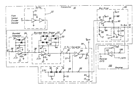
The Transmitter Circuit
With reference now to Fig. 2, this figure depicts;
in schematic form, transmitter 16 that includes a bus driver
circuit 80. Also, Fig. 2 shows the interconnection of
receiver 100 of transceiver 10 to the output of the bus driver
circuit.
Bounded Integrator
VPWM signals from SED 7 enter transmitter 16 at
terminal A and route through a conventional buffer 22 and out
of terminal B to a bounded integrator 24. Integrator 24
produces at an output port C symbol signals having edges with
lengthened rise and fall times, reduced amplitudes and
established trigger point voltages. These parameters maintain
each symbol length equidistant with respect to the pulse width
of the symbol expressed in the square-wave input waveform.
Integrator 24 produces at port C inverted, linear, and bounded
pulses symmetrical about the trigger-voltage level of the
pulse edges in response to square-wave signals at the
inverting input terminal of operational amplifier 26. A
reference voltage of about 2.5 Vdc applies to a non-inverting
'input terminal of amplifier 26 having a chosen voltage gain.
,.
4
s ,
2~~.9~88
This reference voltage establishes the trigger-point-voltage
from whig~ each rising pulse edge extends about 0.5 Vdc above
and each falling edge extends about 0.5 Vdc below the trigger-
point voltage forming bounded voltage levels. Diodes 32 and
34 connected in the feedback loop of amplifier 26 accomplishes
the bounding function. By fixing the trigger point at a fixed
voltage and by bounding the amplitude of the pulses,
substantially equal voltage amplitudes above and below the
trip points result. This operation changes square wave pulses
into trapezoidal pulses. ,
Bounded Waveshaper
Increasing the curvature of the pulse corners of the
waveform at point C provides further reductions of EMI on bus
18. The output signal from bounded integrator 24 at point C
l5 encounters input resistor 38 of a conventional op-amp inverter
circuit 42 of the.bounded waveshaper device 36. As in
conventional op-amp inverters, both input and feedback signals
apply at the inverting input terminal of op-amp 42.
Due to op-amp restraints, the voltage at the inverting input
0 (Vn) must equal the voltage at non-inverting input (Vp) of the
op-amp 42. Since Vp, in this configuration equals 2.5 Vdc,
any voltage change of Vn changes with respect to Vp rather
than a ground offset voltage. Thus, if input resistor 38
senses a negative directed ramp voltage from integrator 24,
5 then op-amp inverter 42 will produce a positive directed ramp
voltage of closed loop gain (K) referenced about 2.5 vdc, the
trip-point voltage. If input resistor 38 senses a positive
directed ramp voltage, then op-amp inverter 42 will produce a
negative directed ramp voltage of closed loop'gain(-K)
0 referenced about the trip-point voltage.
,.
5
a
21~.~488
Voltage Gain Reduction
Also, waveshaping device 36 employs, along with the
op-amp inverter 42, voltage gain reduction circuits to further
increase the curvature of pulse corners of waveforms during
the waveshaping process. Resistor 44 and diode circuits 46
and 48 form the voltage gain reduction circuit which shunts
feedback resistor 40. This voltage gain reduction circuit
reduces clpse loop gain when negative or positive directed
ramp voltages appearing at the output of op-amp inverter 42
reaches a first predetermined voltage level.
Bounding the Voltage Gain Reduction
Along with voltage gain reduction, bounding the
amplitudes of the reshaped pulse corners occurs. When the
negative or positive directed ramp voltage reaches a second
predetermined level, forward biasing bounding diodes 50 or 52
,.,.-w.
causes the ramp voltages to level off to the clamping voltage
established by the bounding diodes 50 or 52 and the
complimenting diode circuits 46 or 48. Hence, a reshaped
output waveform signal appears at point D which includes
:0 increased curvature corners and increased amplitudes of the
pulses with respect to the trip-point voltage.
Voltage To Current Converter
The reshaped output pulse signals at point D enter
voltage-to-current converter device 54 and exit as programmed
:5 current-sink signals used by an associate device discussed
infra. Illustratively, for this illustrated symbol pulse, the
pulse signal at point D has a 1.60 VDC offset, an amplitude of
1.8 Vp_p, a trip-point voltage of 2.50 VDC and~a pulse width
(PW) remaining at 64 ~s.
6
t
a
I
A voltage divider network consisting of resistors 56
and 57 receives the pulses from point D, halves the amplitude
to 0.9 Vp_p, with a 0.8 VDC offset, a 1.25 trip-point voltage
and a 64 us PW and then applies the lowered signal to a non-
inverting input terminal of a non-inverting op-amp 58.
A sensing resistor 64 used for feedback control of
the output current responds to a pulse in the emitter circuit
of an NPN buffer transistor 60 of about 1.60 Vp_p with
respect to signal ground 12.
An offset voltage circuit consisting of diodes 78,
74 and 76, along with resistors 72 and 70, provide a fixed
offset voltage of about 1.60 VDC at the cathode of diode 76~.
Resistor 68, part of the feedback circuit along with feedback
resistor 66, causes a corresponding pulse near 1.60 Vp_p with a
0.80 VDC offset at the inverting input terminal of op-amp 58.
Op-amp 58 outputs a pulse of about 2.5 Vp_p, in phase
with the pulse at the non-inverting input terminal, in
response to the voltage difference between the input pulses at
the non-inverting and inverting input terminals. This
reaction subtracts 1.60 VDC from the signal at point D causing
the trip-point to occur at about 0.9 VCD at the emitter of
transistor 60. The output voltage of op-amp 58 supplies base
current to the NPN buffer transistor 60 through base resistor
62. Emitter voltage of transistor 60 generates a feedback
voltage across current sampling resistor 64 of a chosen value
and a system ground potential. Output current of the circuit
routes through sampling resistor 64 and feedback current
routes through feedback resistor 66. Any tendency for the
output current to change will appear as a change in the
emitter voltage of transistor 60. This change is fed back to
an inverting input terminal of op-amp 58 through feedback
'resistor 66 resulting in a correction which restores both the
,.
7
21~.~~88
emitter voltage and the output current to quiescent close-loop
values.
Bus Driver Circuit
The bus drive circuit 80 operates as a voltage
variable current source circuit. The variable voltage across
current sensing resistor 64 of voltage-to-current circuit 54
enters the-~on-inverting terminal of difference op-amp 81.
Op-amp 81 compares the variable voltage to a divided-down
emitter voltage of bus driver transistor 90. Resistors 82 and
l0 84 form the dividing network. The voltage at the inverting
terminal results from an output current from op-amp 81 which
varies the current of the input loop of transistor 90. The
input loop includes resistors 86, 84, and 82.
The output loop of transistor 90 includes current
from Vbatt that flows through resistor 88 and from collector
to emitter to bus 18. Resistor 92 and capacitor 94 form the
termination network il of bus 18.
If current from op-amp 81 causes the collector-to-
emitter voltage (Vce) of transistor 90 to reach nearly zero,
then transistor 90 saturates and the maximum current that can
-- - ~ flow in the output loop flows onto bus 18. Otherwise,
transistor 90 operates in the active or amplifying mode
provided the amplifying factor (B) times tl~e base current Ib
stays less than the maximum saturation current (I~,sat).
However, if the base-to-emitter voltage (Vbe) of transistor 90
goes below the turn ON voltage (Vt), then very little, if any,
current will flow in the output loop. This causes transistor
90 to operate in the cutoff mode. The resulting waveform will
yield amplified pulse signals at bus 18 with drip points
occurring around 3.875 VDC with the symbol timing remaining at
X64 its.
..=
,.
g
2~.~.~488
Receiver Circuit
Current on twisted-wire bus 18 provides trapezoidal
signals that preserve substantially the original symbol
information at the trip points between pulse edges. Receiver
100, consisting of comparator 101 biased by resistors 102 and
104 to trigger at the trip-point of the pulses, receives these
trapezoidal signals. Comparator 101 triggers to convert the
trapezoida~..signals into digital pulses, used by SED 7 of Fig.
1, to generate digital messages that route to each
microcontroller 5 in each node 4-4.
Wayeform Diactrams
To further explain the operation of system 10, refer
now to waveform diagrams of Figs. 3A through 3F. Fig. 3A
illustrates the VPWM symbol signal that enters transmitter 16
of Fig. 1 from SED 7. Symbol data in square wave pulses
entering transmitter 16 have pulse widths varying from about
16 ~s to as much as 1024 ACS. Pulses in Fig. 3A depict a
dominant short symbol having a pulse width of 64 its.
Fig. 3B illustrates the same symbol message depicted
in Fig. 3A at the output of buffer 22 and at point B of Fig.
2. However, Fig. 3C shows the trapezoid signal at the output
of bounded, integrator circuit 24 of Fig. 2.
Fig. 3D shows the trapezoid signal with its edges
reshaped at the extremities of the pulses edges, with some
gain, after passing through the bounded waveshaper circuit 36
of Fig. 2. While Fig. 3E shows the pulses appearing in the
feedback network of the Voltage-to-Current Converter 54, these
pulses appear across the terminals of sensing resistor 64.
Fig. 3F depicts the pulses at the dutput of Bus
Driver 90. The pulses have a voltage amplitude of about 4
9
' ~ 21~.~~8~
times that a
ppearing across sensing resistor 64 in voltage-to-
current~converter 54.
It is to be understood that the above-described
embodiment mainly illustrates the principles of the present
invention. Although a combination discrete
component/integrated circuit embodiment is disclosed, a
combination integrated circuit/firmware/software equivalent
could be developed. One skilled in the art may make changes
and modifications to the embodiment disclosed herein and may
l0 devise other embodiments without departing from the scope
and essential characteristics thereof. y
i~hat is claimed is:
"