Note: Descriptions are shown in the official language in which they were submitted.
2 1 1 ~ 7
SEMICONDUCTOR DEVICE CAPACITOR AND
METHOD FOR MANUFACTURING THE SAME
Back~round of the Invention
The present invention relates to a capacitor of a
semiconductor device capacitor and a method for manufacturing
- the same, and more particularly to a stacked capacitor of a
semiconductor device having an increased cell capacitance and
a method for manufacturing the same.
In a dynamic random access memory (DRAM) cell which
consists of one transistor and one capacitor, an increase in
cell capacitance causes an improvement in reading ability of
the memory cell and a reduction of soft error ratio, to
thereby improve memory characteristics of the cell. DRAM
~~ integration increases by 4 times approximately every 3 years,
whereas the chip area increases only by 1.4 times.
Relatively, unit memory cell area decreases by 1/3 while the
cell capacitance required by the unit memory cell is regular.
Accordingly, cell capacitance decreases and an electrical
characteristic of a memory device is lowered. Therefore, the
cell capacitance in an unit memory cell needs to be increased
in a limited area.
It is hard to ensure the sufficient and large cell
capacitance in the limited area in the conventional capacitor
structure. Therefore, a lot of methods for forming the
capacitor structure three-dimensionally so as to increase ~-
2 ~
;~ cell capacitance are proposed. There are representative
structures of the three-dimensional capacitors such as a
trench capacitor, stacked capacitor and a stack-trench
capacitor. The trench capacitor is advantageous in ensuring
the large capacitance, however, device characteristics are
decreased by the complicated parasitic transistor effect such
as MOS parasitic transistor effect which exists in the
surface of the trench or the leakage current between the
trenches. Moreover, the manufacturing process is very strict.
On the contrary, the stacked capacitor has less parasitic
- transistor effect compared with the trench capacitor, and is
simple in manufacturing process. However, in the stacked
cap~citor, the capacitance is not sufficient r which gives
-- disadvantage in a high integration. Accordingly, a new
,j
. 15 capacitor having a simple process for manufacturing the
~ device and which can ensure the large cell capacitance is
'i needed.
i T. Ema et al. proposed a new capacitor structure, i.e.,
a fin-structured capacitor, in order to realize the above
l 20 demands (see '3-dimensional stacked capacitor cell for 16M
; and 64M DRA~I' by T. Ema et al., IEDM, 1988, pp. 592-595).
' The fin-structured capacitor is a kind of stacked ~
capacitor, and has a storage electrode comprising multi- ~ -
~ conductive layers and spacers for separating the conduct~ive
! 25 layers. Therefore, the side and bottom surfaces as well as
the upper surface of the conductive layer can be used as an
' 2
:J
! ~,
.'''
2 1 ~
effective area, and the conductive layer can be formed by a
single layer or by the multi-layers. For this reason, the
fin-structured capacitor is an advantageous structure since
the cell capacitance can be easily controlled.
A semiconductor memory device having the fin-structured
capacitor comprises a storage electrode where the four first
conductive layers are formed in symmetry on all sides,
centering around the source region of a transistor, and the
four spacers for separating the four first conductive layers
are formed, and a cylindrical column of the first conductive
layer is formed by connecting the edges of the four
conductive layers, a dielectric film coated all over the
storage electrode and a plate electrode formed all over the
dielectric film.
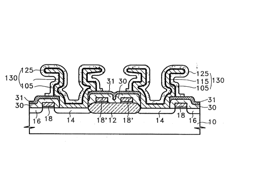
Referring to FIGs. 1 to 3, a method for manufacturing
the fin structured capacitor of the conventional
semiconductor device as disclosed by T. Ema et al will be
explained.
Referring to FIG. 1, a switching transistor comprising a
source region 14, drain region 16 and a gate electrode 18 is
formed in an active region of a semiconductor substrate 10
which is defined into an active region and an isolation
region by a field oxide layer 12. At this time, a word-line
18' elongated from a gate electrode of the adjacent
- 25 transistor is formed on field oxide film 12. Then, a first
etch blocking film 31 is forme* all over semiconductor
i
.,
2 ~ 1 9 rS ~ 7
: r--~
: substrate lo by depositing nitride silicon Si3N4 so as to
hinder an etching process and to insulate gate electrode 18
and word-line 18'. Then, first insulating layer 32 and first
conductive layer 34, for example, a first insulating layer
- 5 having four layers and a first conductive layer having three
- layers in a 4 fin structure, are serially deposited all over
first etch resist film 31, and a photolithography process for
~, forming a contact hole is performed on source region 14, to
thereby form a contact hole 36 for exposing source region 14.
At this time, an insulating material, for example, silicon
dioxide (sio2)~ is used as material that constitutes first ~:~
insulating layer 32, while a conductive material, for ~ :
example, impurity-doped polycrystalline silicon, is used as ~:
~ material that constitutes first conductive layer 34.
Referring to FIG. 2, conductive material same as the
i, ~
~ material that constitutes first conductive layer 34 is
deposited into a predetermined thickness all over the
resultant structure, to thereby form second conductive layer
. 35. Second conductive layer 35 is coupled with source region
. 20 14 of semiconductor substrate 10 via contact hole 36 and
electrically coupled with first conductive layer 34 via the
sidewall of contact hole 36.
Referring to FIG. 3, the deposited first insulating
layer 32, and first and second conductive layers 34 and 35
. 25 are patterned by performing a photolithography process by
; applying a mask pattern (not shown) for forming a storage
','
2 ~
~ .
electrode, to thereby form a storage electrode pattern. Then,
the insulating material remaining between first and second
conductive layers 34 and 35 is removed by wet-etching
process, to thereby form a storage electrode lO0. At this
time, first etching blocking film 31 prevents the previously
formed transistor from being damaged by etchant when the wet-
- etching process is performed. Then, a dielectric film 110 is
formed all over a storage electrode 100 and a conductive
; material is deposited all over the resultant structure, to
thereby form a plate electrode 120. Then, a contact hole
which exposes a drain region 16 is formed on drain region 16
- by a photolithography process. A second etching blocking film
- 42 and a second insulating film 44 are formed all over the
resultant structure and part of drain region 16 is then
exposed. Then, a conductive material is deposited all over
the resultant structure so as to form a third conductive
layer, and a photolithography process is performed by
applying a mask pattern (not shown), to thereby form a bit
line 50.
In a semiconductor memory device comprising a fin-
structure capacitor manufactured by the conventional method,
multi conductive layers and insulating layers are alternately
deposited on a semiconductor substrate and the insulating
layer is etched. Thus, the upper, side and bottom surfaces of
the conductive layers are used as an effective area of a
capacitor. As a result, a capacitor having a large
' ,
. .
- .
i'
capacitance can be formed in the small area of semiconductor
substrate in accordance with high integration.
However, a process for etching the multi-conductive
layers and insulating layers which have largely different
etching selectivity rate is necessary in order to form the
- fin-structure capacitor. The conductive layer and insulating
layer cannot be removed by an one-time etching process. Thus,
an etching process suitable for each layer is necessary,
which causes a complicated processing and an elongated
: 10 processing time. As a result, throughput is lowered. In
general, an etching process which divides the storage
electrode into each cell unit is a dry-etching process.
However, the dry-etching process has to be conducted by
~- varying the etching source in accordance with an etching
selectivity ratio if the object of the etching process is
i-:
changed. In addition, the conductive layer is deposited by 2
times or more so as to increase the cell capacitance.
Therefore, connecting each conductive layer results in the
generation of a contact surface, and the native oxide film is
formed on the contact surface, to thereby lower the
electrical characteristics of a memory device. Moreover, the
height of from the substrate surface to the uppermost portion
of a capacitor is increased as the number of fins is
increased so as to increase the cell capacitance. Thus,
problems are caused by the high step coverage when the
metalization processing is performed. As a result, memory
.~
."
,'' ' ~
~:,
.'` :
2 ~ 7
.
device reliability is lowered.
Meanwhile, U.S. Patent No. 5,142,639 discloses an -~
improved fin-structured capacitor. FIG~ 4 is a sectional view
of a capacitor shown in the above U.S. Patent. Referring to
FIG. 4, reference numerals the same as those of FIG. 1 to
FIG. 3 denote the same member. The semiconductor memory -
device having the above-described fin-structured capacitor
comprises a first insulating film 20, a second insulating
film 21, a storage electrode 25, a dielectric film 26 and a
plate electrode 27 on an insulating film 19 which insulates
gate electrode 18 and word-line 18' and also comprises a
hierarchical structure where dielectric film 26 and storage
electrode 25 are piled one another.
Since the fin-structure forms a storage electrode by a
single conductive layer differently from the conventional
method described with reference to FIGs. 1 to 3, a leakage
current caused by an intermediate material like a natural
oxide material can be prevented. However, the side surface of
the storage electrode cannot be used as an effective
capacitor region, to thereby limit the increase of the cell
capacitance.
In addition, improved fin-structure capacitors are
disclosed in U.S. Patents No. 4,974,040 (Taguchi et al.),
5,071,781 (Seo et al.), 5,053,351 and in U.S. Patent No.
5,164,337 (Ogawa et al.). However, since capacitors having
the improved structure form a storage electrode by forming a
2 ~
plurality of conductive layers, characteristics are degraded
by a native oxide film and the process becomes complicated.
Summary of the Invention
Accordingly, it is an object of the present invention to
provide a capacitor of a semiconductor device formed of a
single conductive layer and which makes it possible to
improve the reliability and the capacitance.
It is another object of the present invention to provide
a method for manufacturing a capacitor of a semiconductor
device suitable for manufacturing the capacitor of a
semiconductor device formed of a single conductive layer by
using insulating materials having different etching rates.
To accomplish the above objects, there is provided a
capacitor of a semiconductor device comprising a storage
electrode formed of a single conductive layer and having a
lower portion connected to a predetermined portion of a
semiconductor substrate and with a body elongated upward from
the lower portion, and which has at least one convex portion
in an middle portion of the body so as to increase a
capacitance thereof; a dielectric film formed inside and
outside of the storage electrode; and a plate electrode
formed in the dielectric film. It is desirable for a --
capacitor of the present invention to comprise a horizontally
elongated fin-structured portion in the uppermost portion of
the body
.
2 ~ 7
According to an embodiment of the present invention, the
outside bottom surface of the convex portion and the outside
surface of the lower body under the convex portion are formed
being in contact to the structure formed on the semiconductor
substrate.
: According to another embodiment of the present
invention, the elongated dielectric film and plate electrode
are formed on the bottom surface of the outside of the convex
portion.
To accomplish another object of the present invention,
there is provided a method for manufacturing a capacitor of a
semiconductor device, the method comprising the steps of:
serially depositing a first material and a second
material whose etching rates are different with respect to a
first isotropic etching process all over the semiconductor
substrate where an insulating layer for insulating a
transistor which consists of a source region, a drain region
and a gate electrode is formed, to form a first material
layer and a second material layer;
partially etching the first material layer and the
~-: second material layer which are formed on the source region
and the insulating layer, to form a contact hole for
partially exposing the source region;
- partially and isotropically etching the side of the
. 25 first material layer exposed by the contact hole via the
. first isotropic etching process, to form a convex space
.,
~., 9
. ~
! ~
',':1
I !
` 2~9~7
- portion;
forming a first conductive layer all over the structure
including the contact hole and the convex space portion;
- defining the first conductive layer into each cell unit
to form a storage electrode pattern;
removing the first and second material layers to expose
the storage electrode pattern; and
forming a dielectric film and a plate electrode on the
storage electrode pattern.
The step of removing the first and second material
layers is performed by a second isotropic etching process by
using an etchant having a similar etching rate for the first
and second material layers, which is desirable~
According to an embodiment of the present invention, the
method of the present invention further comprises the step
of: forming a third material layer on the insulating film by
depositing a third material prior to the formation of the
first material layer. Material whose etching rate is
different from that of the first material and second material
with respect to an arbitrary isotropic etching process, is
used as a third material. The elements formed in the lower
portion can be protected during an arbitrary isotropic
etching process by forming a third material layer.
It is preferable to have the first material whose
etching rate is the same with that of second material with
respect to a predetermined anisotropic etching process and
''.
~'
2~19~
whose etching rate is different from that of second material
; with respect to a first isotropic etching process.
- Accordingly, the contact hole can be easily formed, and the
first material layer is isotropically etched, thereby forming
the convex space portion easily.
In addition, it is desirable to have the thickness of
the first and second material layers to be more thick than
double the thickness of the conductive layer. Thus, the
convex portion of the storage electrode can be easily formed
by considering the thickness.
According to another embodiment of the present
invention, the second material is deposited prior to the step
of serially depositing the first and second material layers,
to thereby form a lower second material layer. Then, the
lower second material layer is also removed when the first
and second material layers are removed, to thereby expose the
lower portion of the convex portion of the storage electrode
pattern.
According to an embodiment of the present invention, the
step of serially forming the first material layer and the
second material layer has to be repeated at least twice.
~ Thus, a multitude of convex portions are provided to a
i~ storage electrode pattern, which increases the cell
capacitance.
- 25 According to an embodiment of the present invention, the
' convex portion is extended by repeating the first isotropic
~'' 11
-
. .
~19~7
etching process at least twice. The convex portion can be
extended to the degree that it does not affect the adjacent
peripheral structure.
The contact hole can be formed by an anisotropic etching
process, and also can be formed by performing an isotropic
etching first and an anisotropic etching secondly.
Since the storage electrode is formed of a single
conductive layer, a degradation of electrode characteristics
caused by the formation of a native oxide film can be
- 10 prevented. Further, the upper, side and bottom surfaces of a
storage electrode can be used as an effective capacitor area,
thereby easily increasing the cell capacitance. As a result,
a reliable capacitor having a high capacitance can be
- obtained.
... .
Brief Description of the Drawinqs
- The above objects and other advantages of the present
:;
invention will become more apparent by describing in detail a
preferred embodiment thereof with reference to the attached
drawings in which:
FIGs. 1 to 3 are sectional views showing a method for
manufacturing a fin-structured capacitor of a semiconductor
~ device according to a conventional method;
':
FIG. 4 is a sectional view showing an embodiment of a
conventional modified fin-structured capacitor of a
semiconductor device;
12
. .
2 1 ~ 7
FIG. 5 is a section view showing an embodiment of a
capacitor of a semiconductor device according to the present
nvent l on;
FIGs. 6 to 10 are sectional views illustrating a first
embodiment of a method for manufacturing a capacitor of a
semiconductor device according to the present invention;
FIGs. 11 and 12 are sectional views illustrating a
second embodiment of a method for manufacturing a capacitor
of a semiconductor device according to the present invention;
and
FIGs. 13 and 14 are sectional views illustrating a third
embodiment of a method for manufacturing a capacitor of a
semiconductor device according to the present invention.
,
Detailed Description of the Invention
The present invention will be explained in more detail
with reference to the attached drawings.
. FIG. 5 is a sectional view showing an embodiment of a
capacitor of a semiconductor device of the present invention.
Referring to FIG. 5, the reference numerals same with those
of FIGs. 1 to 4 denote the same members. A storage electrode
~, 105 of the semiconductor memory device comprises a lower
portion connected to a predetermined portion (source region
of a transistor) of the semiconductor substrate where the
lower structure (for example, a transistor) is formed and a
- 25 body elongated upwards from the lower portion. The middle
13
.,
~, ~
,
, , .
2 ~ 7
,.
portion of the body comprises a convex portion, and
therefore, is shaped into a vase whereby the surface area of ~-
the storage electrode is increased. A horizontally elongated
fin structure is formed in the uppermost portion of the body.
A plate electrode 125 is formed on the exposed entire
surface, i.e., on the internal and external surfaces, of
storage electrode 105 with a dielectric film interposed
therebetween. Referring to storage electrode 105 shown in
FIG. 5, the bottom surface of the lower portion of the convex
portion and part of the lower body of the convex portion are
- connected to insulating film 30 and etching blocking film 31
which are formed on semiconductor substrate 10. As shown in
FIG. 5, dielectric film 115 is formed on the inside and outer ~-
surface and on the upper portion of the body above the convex
portion, which are used as an effective area of a capacitor.
A method for manufacturing a capacitor of a
semiconductor device according to the present invention will
be explained in more detail by the following embodiments.
Embodiment 1
FIGs. 6 to 10 are sectional views illustrating a first
embodiment of a method for manufacturing a capacitor of a
semiconductor device according to the present invention.
FIG. 6 shows the step of forming a transistor on a~
semiconductor substrate 10. In more detail, a field oxide
film 12 for defining an active region and an isolation region
' ,
;'
<
2 ~
\
~ is formed on semiconductor substrate 10. Then, an oxide film
; is formed all over the resultant structure so as to form a
gate oxide film. Then, a conductive material is deposited on
- the oxide film for forming a gate electrode. Then, the oxide
film and conductive layer are patterned by a photolithography
process, to thereby form a gate electrode 18. At this time,
word line 18' connected to a gate electrode of the adjacent
transistor is formed on field oxide film 12. Then, for
example, an N-type impurity ion, -is doped all over the
resultant structure using gate electrode 10 as a mask when
- the semiconductor substrate is doped with a P-type
impurities, thereby forming source region 14 and drain region
~ 16. Thus, a transistor comprising source region 14, drain
; region 16 and gate electrode 18 is formed. Then, insulating
material, for example, high temperature oxide (HT0), is
deposited all over semiconductor substrate 10 where a
transistor is formed, so as to insulate the transistor, to
thereby form an insulating layer 30.
FIG. 7 shows the step of sequentially forming a first
material layer 33 and a second material layer 37 all over
semiconductor substrate 10. A silicon nitride layer is
deposited to a thickness of approximately 200A to 500A all
over the resultant structure where the transistor is formed,
,:
to thereby form etching blocking film 31. A first material
~` 25 and a second material whose etching rate are different with
.i respect to a first isotropic etching process and whose
: . .
.
~: 1
`~ 2~9~7
etching rate are similar with respect to a second isotropic
- etching process, are serially deposited to a thickness of
approximately 1,oOOA to 10, oooA, to thereby form first
material layer 33 and second material layer 37. When a boron
phosphorous silicate glass (BPSG) is used as a first
- material, a high temperature oxide (HT0) can be used as a
- second material. When BPSG is used as first material layer
33, the successive process can be smoothly performed by a
- planarization process, i.e., BPSG reflow process, which is
desirable. In addition, it is desirable to form the thickness
of first material layer 33 to be further thicker, for
example, by 2 times or more, than that of a first conductive
layer (reference numeral 41 of FIG. 9) for forming a first
electrode of the capacitor. Materials (say "A" and "B")
having the same etching rate with respect to a predetermined
anisotropic etching and different etching rates (it is
desirable that the etching rate of "B" is 8 or higher when
the etching rate of "A" is 1) with respect to a predetermined
first isotropic etching process, have to be used for
constituting first material layer 33 and second material
layer 37. When an isotropic etching process is performed by a
wet-etching method where an etchant such as standard cleaning
1 (SC1 : etchant where NH40H, H202 and HzO are mixed in a
ratio of 1:4:20), which shows an etching rate of first
material layer 33 which is much higher with respect to the
, predetermined isotropic etching process as compared with
.,; .
16
.
~, .
., .
.,
2 ~
,,. ~
second materlal layer 37, is used, it is desirable to use
" BPSG film as first material layer 33 and ~TO film a~ second
material layer 37 (here, the etching rate of HTO film with
respect to SC1 is approximately 4.4A/min, and an etching
rate of BPSG film is approximately 35.2A/min). When an
isotropic etching is performed by a wet-etching method using
hydrofluoric acid (HF), it is desirable to use spin-on-glass
- (SOG) film as first material layer 33 and HTO film as second
-~ material layer 37 (here, the etching rate of SOG film to HF
is approximately 5~oooA/min to 9~oooA/min and that of HTO
film is approximately 90A/min). As for a material that
- constitutes etching blocking film 31, it is desirable to use
a material whose etching rate is different from that of the
material constituting the first material layer, with respect
to the predetermined isotropic etching aiming to partially
remove the first material layer, such as a nitride which is
,,
mentioned above. Moreover, a cell capacitance can be
controlled by varying the times of depositing first and
second layers. When a capacitor is formed after a bit line is
;20 formed, the thickness of first and second layers 33 and 37
can be increased, to thereby increase a cell capacitance.
"
. FIG. 8 shows a step of forming a contact hole 39 and a
- space-portion 38. Layers formed on source region 14 of a
- transistor are partially removed using a mask pattern (not
~' 25 shown) for forming a contact hole which aims to make a
storage electrode contact to source region 14 of a
17
, ,i
!
.... .
2 1 ~
transistor, to thereby form contact hole 39. When materials
that constitute first and second material layers 33 and 37
have the same etching rate with respect to an anisotropic
etching process for forming contact hole 39, an etching gas
doesn't need to be changed according to the change of the
etching object, as it did in the conventional method, which
simplifies the process. After an isotropic etching is
performed by wet-etching method, an anisotropic etching is
performed by a dry-etching method, to thereby form contact
- 10 hole 39. Thus, an aperture of the upper portion of contact
hole 39 is formed large, to thereby remove a void which may
occur in the succeeding process.
- Then, first isotropic etching process having Æirst
material layer 33 as an etching objective, using wet-etching
method is performed all over the resultant structure, to
thereby form space portion 38. The side portion oÆ first
material layer 33 exposed by contact hole 39 in the first
isotropic etching process is partially etched and removed.
Here, space portion 38 means a portion where the exposed side
portion of first material layer 33 is removed. In the present
embodiment, an wet-etching process using standard cleaning
(SC1) is performed for twenty to fifty minutes, to thereby
form space portion 38.
FIG. 9 shows a step of forming a storage electrode.
After the step of FIG. 8 is performed, a conductive material,
for example, an impurity-doped polycrystalline silicon, is
18
., .
.' '
r~
deposited to thereby form a first conductive layer 41 having
a thickness of approximately half of the thickness of the
first material layer, for example, approximately sooA to
5, oooA, all over the resultant structure. Then, a
photoresist pattern 43 is formed by applying a mask pattern
(not shown) for forming the storage electrode. First
conductive layer 41 is defined into each cell unit by using
the photoresist pattern as an etching mask, thereby
completing a storage electrode (reference numeral 105 of FIG.
10). In order to form the storage electrode, multiple
conductive layers and insulating layers having large
- different eching rates from each other have to be etched by
the etching process appropriate for each layer in the
conventional method. Therefore, the process is complicated
and the process time is elongated. However, in the present
embodiment, the process is much more simplified and process
time is considerably reduced since only first conductive
layer 41 is necessary to be etched.
FIG. 10 shows the step of forming a dielectric film 115
' 20 and a plate electrode 125. All the remaining first and second
material layers 33 and 37 are removed by performing a second
isotropic etching by a wet-etching method all over the
resultant structure where storage electrode 105 is formed,
thereby exposing the side surface of storage electrode 105. -
At this time, the wet-etching process is performed for
approximately five to fifty minutes by using a wet-etching
19
., .
211~7
etchant where first and second material layers have similar
etching rate, for example, LAL500, buffered oxide etchant
(BOE; mixture of NH4F and HF) or surfactant buffered oxide
etchant (SBOE; NH4F and HF mixture with a surfactant added).
Then, an insulating material, for example, nitride/oxide
(NO), oxide/nitride/oxide (ONO) or tantalum pentaoxide
(Ta2Os) is deposited all over storage electrode 105, thereby
forming dielectric film 115. Then, a conductive material such
as an impurity-doped polycrystalline silicon is deposited all
over the resultant structure, thereby forming a second
conductive layer. Then, a photolithography process adapting a
mask pattern (not shown) for forming a plate electrode is
performed, to thereby form plate electrode 125. In the
present embodiment, all the remaining first and second
. 15 material layers 33 and 37 are removed by the second wet-
. etching process. Therefore, all the inner and outer surfaces
of storage electrode 105 which contact the first and second
material layers are exposed, to thereby increase the area of
an effective capacitor.
Embodiment 2
FIGs. 11 and 12 are sectional views illustrating a
second embodiment of a method for manufacturing a capacitor
of a semiconductor device according to the present invention.
In the present embodiment, all processes are similar with
that of embodiment 1, except that an additional second
.,
.,
2 ~ 7
-~ material layer is formed before the first material layer is
formed in embodiment 1.
FIG. 11 shows a step of forming contact hole 39 and
space portion 38. According to a method described with
reference to FIG. 6, insulating layer 30 and etching blocking
film 31 are serially formed on semiconductor substrate 10
where a transistor is formed. Then, a first second material
layer 37a is firstly formed all over the resultant structure,
and first material layer 33 and a second second material
layer 37b are serially formed on first second material layer
37a. At this time, as for the first material layer and first
and second second material layers 37a and 37b, materials the
same as that explained with reference to FIG. 6 is used. That
is, it is preferable to use BPSG for example for first
material layer 33 and HT0 for first and second second
material layers 37a and 37b.
Then, in the same manner as explained with reference to -
FIG. 8, contact hole 39 is formed by removing the material
deposited on source region 14 of the transistor. Then, a
first wet etching process where first material layer 33 is an
etching-objective is performed all over the resultant
structure, thereby forming space portion 38.
FIG. 12 shows a step of completing the formation of a
- capacitor. After the step described with reference to FIG. 11
is performed, storage electrode 105 is formed in the same
manner as explained in FIGs. 9 and 10. Then, all the
21
;' .
2 ~ 7
remaining first material layer 33 and first and second second
material layers 37a and 37b are removed by a second wet-
etching method. Then, dielectric film 115 and plate electrode
- 125 are formed all over storage electrode 105, thereby
completing formation of a capacitor.
According to the present embodiment, the area of an
effective capacitor can be increased by exposing the lower
portion of the convex portion of storage electrode 105 formed
in embodiment 1, i.e., the portion which contacts to a
predetermined surface of etching blocking film 31.
; Embodiment 3
FIGs. 13 and 14 are sectional views illustrating a third
embodiment of a method for manufacturing a capacitor of a
semiconductor device according to the present invention. In
the present embodiment, the processes are the same with those
of embodiment 1 except that the space portion for forming a
storage electrode is further extended by repeating the first
wet etching process in embodiment 1.
FIG. 13 shows the step of forming a space portion. First
wet etching process having first material layer 31 as an
etching-objective is performed all over the resultant
structure having contact hole 39 obtained according to the
method explained with reference to FIGs. 6 to 9, to thereby
form the space portion as shown in FIG. 8 (reference numeral
38 of FIG. 8 denotes the portion which corresponds to
;~
'
2 1 ~ 7
reference numeral Bl of FIG. 13). Then, a space portion B2
where portion B1 is further extended, is formed by performing
the first wet etching process again. At this time, space
portion B2 can be extended up to the size which may not
disturb the formation of the peripheral structure (for
example, the bit line when a bit line is formed after a
capacitor is formed) by repeating the first wet-etching
process.
FIG. 14 shows the step of completing the formation of a
lo capacitor. After space portion B2 is formed, storage -
electrode 105, dielectric film 115 and plate electrode 125
are formed in same manner as explained with reference to FIG.
10, thereby completing formation of a capacitor.
According to the present embodiment, the area of the
effective capacitor can be increased due to the enlargement
of space portion B2. Since the area of the effective
capacitor is increased mainly in the horizontal direction, an
increase of cell capacitance can be achieved even without
largely increasing the step coverage in the vertical
direction. The present embodiment can be applied together
with embodiment 2.
According to a method for manufacturing a capacitor of
semiconductor device of the present invention, first and
- second materials whose etching rates are the same with
respect to a predetermined anisotropic etching process and
':
. :,
2~19~7
- .-
whose etching rates are different from each other with
; respect to a predetermined isotropic etching process, are
;- deposited all over the semiconductor substrate where a lower
structure (for example, when a bit line is formed before a
transistor and capacitor are formed, the bit line included)
is formed, to thereby sequentially form a first material
; layer and a second material layer. Then, a contact hole
exposing a portion of the source region of a transistor is ;~
formed. Thereafter, a convex space portion is formed by
partially removing one material layer of the two material
layers exposed by the contact hole using a first isotropic
etching method. Then, a conductive material is deposited so
as to form a storage electrode and then all the first and
second material layers are removed by a second isotropic
etching process. The outer sidewall of the storage electrode
which contacts to the two material layers is exposed, to
thereby easily increase the cell capacitance. Thus, the
outside surface of the storage electrode can be utilized as
an effective capacitor area, to thereby increase the cell
capacitance. Further, in the conventional method, a dry-
etching process (an etching gas has to be changed in
; accordance with the change of the etching-objective in the
conventional method) for an anisotropic etching has to be
performed several times; however, the dry-etching process is
reduced to one time in the present invention, which
simplifies the process. Moreover, since the storage electrode
:
24
',
..
, :
.. .
2 ~ 7
is formed of a single conductive layer, the leakage current
caused by the intermediate material like a native oxide film
can be prevented and the surface area of the storage
electrode can be increased in the horizontal direction. Thus,
step coverage in the vertical direction is not much
increased, which enables the subsequent metalization process
to be achieved reliably. As a result, a high integrated
semiconductor memory device having a high reliability can be
manufactured.
It will be understood by those skilled in the art that
the foregoing and other changes in form and details can be
made therein without departing from the spirit and scope of
the invention.