Note: Descriptions are shown in the official language in which they were submitted.
1 2~~.~~~~1
RJB/DHH/91 A236
APPARATUS FOR RAPID PLASMA TREATMENTS AND METHOD
The present invention relates to the plasma treatments of substrates, and more
particularly to the rapid plasma enhanced deposition of silicon oxide based
thin
films on substrates to provide gas transmission barriers useful for packaging
applications.
Plasma polymerisation, sometimes designated "plasma enhanced chemical
vapour deposition," or "PECVD," has been a known technique to form films on
various substrates. For example, mixtures of silane with or without oxygen,
nitrous oxide or ammonia have been plasma polymerised to form silicon oxide
films.
In general, the films formed from organo-silicons have typically been formed
at a
relatively low deposition rate (as compared with, for example, magnetron
sputtering), have tended to be soft, and often have been hazy. The frequent
requirement that the substrate be heated, is also disadvantageous for some
substrates.
A further problem with use of organosilicon compounds in plasma enhanced
deposition has been the variation in polymerisation conditions and lack of
control during the deposition. The traditional method used to control plasma
processes has been the use of power, pressure and flow to monitor and attempt
to control the process. However, these three variables represent inputs and do
not accordingly control the thin films being produced. As a consequence, the
scale-up of such a process is extremely complex.
In early microelectronic PECVD reactors, the plasma was generated between
two parallel, circular electrodes. The wafers were loaded onto the lower,
electrically grounded, electrode. The upper electrode was connected to a rf
~E~rd~~TE.,ET
2~.~.~~~.
2
RJB/DHH/91 A236
generator through an impedance matching network. The reactants were fed in
from a gas ring, entered the plasma region (ie, the region between the
electrodes) at its outer edge, and flowed radially in toward a pumping port at
the centre of the electrode. These reactors have commonly been known as
"radial flow" reactors.
In "inverse" radial flow reactors, the gas inlet has been at the centre of the
lower electrode, with the gas flow directed radially outward. A magnetic drive
assembly permitted rotation of the lower electrode, thus randomising the
substrate position and optimising deposition uniformity.
In hot-wall, batch PECVD systems, the deposition chamber consisted of a quartz
tube placed within a resistively heated furnace. Vertically oriented graphite
slabs carried the wafers in slots. Every other slab was connected to the same
rf
power terminal and a glow discharge was generated between adjacent
electrodes. The reactants were directed along the axis of the chamber tube and
between the electrodes.
More recently, PECVD has been employed to coat large substrates, eg, plastic
containers and long rolls of flexible films for food packaging applications.
In the
process described by Felts and Lopata, US Patent 4 888 199 issued December
19, 1989 of common assignment herewith, plasma polymerisation is used to
deposit silicon oxide based thin films from volatile organosilicon compounds.
Films with reduced permeability to vapours such as water, oxygen, and carbon
dioxide are useful for a variety of applications, one of which is to package
foods. Such films are typically composites of materials. For example, one
layer
is often a flexible polymer, such as a polyethylene or polypropylene, while
another layer is coated on or coextruded with the one layer and serves as a
barrier layer. Barrier layers can generally be viewed as substantially organic
based or substantially inorganic based.
d :. ~ -~:_. : .' ;T ~ .' ~~~T
3 2~~~~~~
RJB/DHH/G'! A236
Plasma assisted or enhanced processes, in addition to coating applications
such
as above described, include plasma etching or cleaning where substrate
surfaces
are modified. Plasma etching, for example, is used in manufacturing intecrated
electronic circuits.
A variety of equipment for plasma treatments are known. For example, : ~
Patent 4 968 918, issued November 6, 1990, inventors Kondo et al, disc;~ses a
plasma treating apparatus having a plurality of powered electrodes. The
substrate being plasma treated is passed proximate to the powered elect-~des.
European Patent Specification No. 406 691 A discloses a method of
continuously depositing thin films on substrates by PECVD means. However,
the method (and apparatus) disclosed therein does not incorporate a main
feature of the present case, namely the use of a plasma-facing surface of an
electrode in rolling contact with the substrate.
European Patent Specification No. 299 754 A discloses a further PECVD
deposition method. However, the method (and apparatus) disclosed therein an
unbalanced magnetron to confine a portion of the plasma adjacent the
substrate. Unlike a magnetron, however, in which the electric and magnetic
fields are directly coupled, the present case generally allows the magnetic
and
electric fields to be decoupled to extend the plasma throughout the plasma
volume, thereby allowing gas phase ionisation to occur whilst maintaininc high
energy electron bombardment at the substrate surface.
Figure 1 is a general schematic diagram illustrating a plasma vacuum systam
with which embodiments of the invention can be used; and
Figure 2 schematically illustrates a side sectional view of the reaction
chamber
and its associated equipment utilizing various aspects of the present
invention.
~~~ a ~ a a~T~ ~T
2~~~~~~.
4
RJB/DHH/91 A236
In one aspect of the invention, a plasma treating apparatus comprises a plasma
treating apparatus comprising:
an evacuable chamber;
means for forming a plasma within the chamber, the plasma forming means
including an electrode defining a plasma-facing surface within the chamber;
means for communicating electricity from the electrode to a substrate when the
substrate is within the chamber by placing the plasma-facing surface into
rolling
contact with the substrate and for exposing a continuously changeable portion
of the substrate to plasma during plasma treatment; and,
means for confining the plasma adjacent to the continuously changeable
substrate portion, the confining means including a grounded shield.
The confining means generally confines the plasma at the substrate portion
being plasma treated to within a distance a in combination with the apparatus
elements, for achieving relatively rapid depositions of films that provide gas
barrier properties. The confining means forms a ground plane with respect to
the electrode.
In another aspect of the present invention, a silicon oxide based film is
deposited having vapour barrier properties. Practice of the invention permits
preparation of particularly preferred flexible polymer substrate embodiments
coated to have a permeability to oxygen gas that is less than about 0.1
cc/6.45x10'2m2/day with thin film thicknesses less than about 1000 ~ at
deposition rates greater than about 250 /sec. Such embodiments are useful
where inert, flexible packagings with excellent vapour and gas barrier
properties
are required, such as for serum and blood bags in medical applications and for
food packaging of very oxygen-sensitive foods, at commercial coating rates.
~~x
~~ ~~ E~~~ ~~~~ i
~~~~ ~~1~
RJB/DHH/91 A236
The inventive plasma treating apparatus is useful in coating applications, as
well
as plasma etching or cleaning where substrate surfaces are to be modified. The
best mode contemplated for using the inventive plasma treating apparatus is
where the substrate being treated is due to the preferred configuration of the
system that carries the substrate through the plasma during plasma treatment.
This will be more fully discussed hereinafter.
Various flexible plastics, whether electrically conducting, semi-conducting,
or
non-conducting are suitable and may be coated in accordance with the
invention. For example, various flexible plastics such as
poly(ethyleneterephthalatel (PET) or polycarbonate (PC) resins, useful for
packaging foods, may be coated in accordance with the invention to retard
oxygen, carbon dioxide or moisture permeation. Although thicknesses of
flexible substrates will be up to about 4x10'2mm, the thicknesses are usually
about 2 - 4x10'3mm for food packaging applications.
The inventive apparatus is preferably used to prepare flexible films with
reduced
permeability to vapours such as water, oxygen, and carbon dioxide. It has been
discovered, as described in EP 469 926, published February 5, 1992, inventor
Felts, of common assignment herewith, that gas transmission properties are a
function of film thickness on flexible substrates and surprisingly have an
optimal
range of thickness to provide the maximal barrier properties, with both
thicker
and thinner films outside the optimal range having less desirable barrier
properties. Articles prepared in accordance with the invention preferably are
where a polymer substrate and thin film carried on the substrate together have
a
permeability to oxygen gas that is less than about 0.1 cc/6.45x10'2/m2/day and
the thin film has a thickness less than about 1000 ~1, more preferably less
than
about 600 ~, most preferably the thin film has a thickness between about
100 ~ to about 400 ~ and the coated plastic film has an oxygen permeability of
less than about 0.04 cc16.45x10'2m2/day.
s 2I~.~iT~
RJB/DHH/91 A236
In one embodiment of the invention, a silicon oxide based film with vapour
barrier properties is deposited from a glow discharge plasma derived from a
gas
stream including a volatilized organosilicon compound, oxygen, and an inert
gas.
Although the preferred process has an organosilicon compound as a starting
material, the films therefrom are substantially inorganic as evidenced by
bonding
analysis. However, films that are silicone in nature may be prepared if
desired,
as further described hereinafter. The typical, substantially inorganic silicon
oxide based films deposited in accordance with the invention are characterised
by a high degree of crosslinking (determined by Fourier transform infrared
spectroscopy, or FTIR). Gas stream control for such an embodiment is
preferably by means of plasma diagnostics, as described by US Patent
4 888 199, issued December 19, 1989, inventors Felts and l_opata.
The combination of oxygen component and inert gas component with the
volatilized organosilicon component has been found greatly to increase the
hardness property of thin films. Films prepared either with the organosilicon
combined only with oxygen or the organosilicon combined only with an inert gas
such as helium or argon had a hardness measured by the ASTM D3363-74
(standard test method for film hardness) pencil test of only 2 or 3. By
contrast,
films made with a combination of organosilicon, oxygen, and inert gas in
accordance with the invention have hardnesses by this test of about 7 to about
9+. The numbers reported are based on a scale of 0 to 10 where 0 means the
least scratch resistance, while 10 means there was no damage to the coating
when abraded in accordance with ASTM D3363-74. Accordingly, thin films can
be prepared that are typically harder by a factor of 2 or 3 with respect to
films
deposited with the volatilized organosilicon component in combination with
either oxygen or inert gas.
Suitable organosilicon compounds for the gas stream are liquid at about
ambient
temperature, and when volatilized have a boiling point above about ambient
temperature. These include methylsilane, dimethylsilane, trimethylsilane,
. -. ..;:-::..-.~ e._~~
v.i ~:.r°s~ i W i~ t
7 2~~~~~.~.
RJB/DHH/91 A236
diethylsi(ane, propylsilane, phenylsilane, hexamethyldisilane, 1,1,2,2-
tetramethyl
disilane, bis(trimethylsilyl) methane, bis(dimethylsilyl) methane,
hexamethyldisiloxane, vinyl trimethoxy silane, vinyl triethoxy silane,
ethylmethoxy silane, ethyltrimethoxy silane, divinyltetramethyldisiloxane,
divinylhexamethyltrisiloxane, and trivinylpenta-methyl-trisiloxane.
Among the preferred organosilicons are 1,1,3,3-tetramethyldisiloxane,
hexamethyldisiloxane, vinyltrimethylsilane, methyltrimethoxysilane,
vinyltrimethoxysilane and hexamethyldisilazane. These preferred organosilicon
compounds have boiling points of 71 ° C, 101 ° C, 55.5°
C, 102° C, 123° C,
and 127° C, respectively.
The volatilized organosilicon component is preferably admixed with the oxygen
component and the inert gas component before being flowed into the chamber.
The quantities of these gases being so admixed are controlled by flow
controllers so as to adjustably control the flow rate ratio of the gas stream
components.
The organosilicon compound and oxygen of the gas stream during the
depositing may be, for example, in a flow rate ratio of about 0.1:1.0 and the
inert gas of the gas stream preferably is helium. When the inert gas is
helium,
then a suitable flow rate ratio of organosilicon compound, oxygen and helium
is
about 0.1:1.0:1Ø Other flow rate ratios may be used, however, if desirable.
In addition to organosilicon, oxygen and inert gas in the gas stream, minor
amounts (not greater than about 1:1 with respect to the organosilicon, more
preferably about 0.4 to 0.1:1 with respect to the organosilicon) of one or
more
additional compounds in gaseous form may be included for particular desired
properties. For example, inclusion of a lower hydrocarbon such as propylene
improves many frequently desired properties of the deposited films (except for
light transmission), and bonding analysis indicates the film to be silicon
dioxide
-.a..
'ad.-. y :a '>, -. ,' '; ~ s 4y .
8
RJB/DHH/91 A236
in nature. Use of methane or acetylene, however, produces films that are
silicone in nature. The inclusion of a minor amount of gaseous nitrogen to the
gas stream increases the deposition rate, improves the transmission and
reflection optical properties on glass, and varies the index of refraction in
response to varied amounts of N2. The addition of nitrous oxide to the gas
stream increases the deposition rate and improves the optical properties, but
tends to decrease the film hardness. A particularly preferred gas stream
composition has 500 to 1,000 SCCM organosilicon, 3000 to 8000 SCCM 02,
and 3000 to 5000 SCCM He.
Although the inventive apparatus that will now be more specifically described
with reference to Figures 1 and 2 is preferably used to reproducibly deposit
adherent, hard silicon oxide based thin films from a plasma that is derived
from
a gas stream including organosilicon, oxygen, and inert gas, one can also use
the inventive apparatus for plasma etching or cleaning or non-SiOx chemistry.
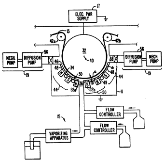
Turning to Figure 1, a plasma treating apparatus 10 embodiment is
schematically illustrated that includes an enclosed chamber 11 in which a
plasma is formed and in which a substrate, such as substrate 13, is
continuously introduced for plasma treating. One or more gases are supplied to
the chamber 11 by a gas supply system 15. Where, for example, one wishes to
prepare articles with vapour barrier properties, then gas supply system 15 can
supply the oxygen component, inert gas component and volatilized organosilicon
component. However, if one wishes to plasma etch, for example, then gas
supply system 15 can supply oxygen, or oxygen and helium, or a suitable
etchant gas mixture ieg. oxygen and a halogen components?.
An electric field within chamber 11 i's created by a power supply 17. Power
supply 17 typically provides about 8 kW during plasma treatments such as
vapour barrier coating. Chamber 11 is evacuable, and a low pressure is
maintained by a pumping and pressure control system 19. chamber 11 and the
_ .,~ ,,~ . ~,:~= '
.,' '.~J!~ . .. . .. .. s '~
CA 02119561 2001-02-21
9
RJB/DHH/91 A236
pumps/pressure control system 19 should be capable of maintaining a pressure
of less than about 13.3Pa (0.1 torr) during plasma treatment and more
preferably 6.6Pa (0.05 torr).
An optical emission spectrometer 21 is preferably connected through an optical
fibre light transmission medium 23 to the chamber 11 in some appropriate
manner to couple the visible and near visible (especially the ultraviolet
range)
emission of the plasma to the spectrometer. A quartz window 25 in a sidewall
of the reaction chamber can be used to optically couple the plasma emission
with the exterior fibre medium 23. A general system control 27, including a
computer controlled portion, is connected to each of the other components of
the system in a manner to receive information from them and to send
controlling
commands to them. Control of coating processes through use of readings from
spectrometer 21 is more fully described by US Patent 4 888 199.
A more detailed explanation of chamber,11 will now be given with respect to
Figure 2 (where a PECVD, or plasma polymerisation, process as the plasma
treatment is exemplified).
chamber 11 includes means 30 for forming a plasma within chamber 11. The
plasma forming means 30 includes an electrically powered electrode 32 defining
a plasma-facing surface 34 within chamber 11. Plasma forming means 30 in
the embodiment illustrated by Figure 2 also includes a source of film-forming
gas, such as the gas supply system 15 with gas inlet 36.
Substrate 13 is continuously fed into, through, and out of chamber 11 as a
strip, or web, with. a continuously changeable portion of substrate 13 being
exposed to the plasma so as to be plasma treated, such as coated with a thin
film having vapour barrier properties. , While a continuously changeable
portion
of substrate 13 is being plasma treated, substrate 13 is also negatively
biased.
~~.~.~~~1
RJB/DHH/91 A236
These two functions are achieved by a means 38 for communicating electricity
from electrode 32 to substrate 13 when within chamber 11 and for exposing a
continuously changeable portion of the substrate to the plasma during plasm
treatment. Negative bias assists in focusing the deposition onto the substrate
and permits deposition with lower power settings. However, when the
substrate is conductive, then one can bias substantially directly (that is,
without
a separate electrode).
One embodiment of communicating and exposing means 38 is wherein electrode
32, or at least its plasma-facing surface 34, is cylindrical, or drum-like,
although
generally arcuate configurations that extend along an axis 40 can be used. The
purpose of such an arcuate, or cylindrical, configuration for plasma-facing
surface 34 is so that a flexible substrate 13 can be placed into rolling
contact
with the plasma-facing surface 34 and thus fed as a web, such as with the
assistance of secondary rollers 42a, 42b which can be adjusted to tension
substrate 13 when fed through the plasma while a negative bias is imposed
upon at least that portion of the substrate being exposed to the plasma at any
one point in time during the plasma treatment. The substrate portion is within
a
confined plasma because a means 44 confines the plasma to a band 46 having
a dimension, or width, as distance o. Distance a extends traversely to plasma-
facing surface 34 and axis 40. As will be discussed and exemplified
hereinafter
in more detail, the plasma confinement is crucial for achieving high
utilisation of
the process gas and power with resultant high deposition rates. Confining
means 44 thus confines the plasma to the continuously changeable portion of
substrate 13 and to within distance a outward (radially outward when surface
34 is cylindrical) from the substrate. Distance o should be not greater than
about 30 centimetres, more preferably be not greater than about 10
centimetres, more preferably is in a range of about 5 centimetres to about 7
centimetres. Distance o preferably is not less than about 1 centimetre because
otherwise the plasma will tend to be extinguished.
:~i/,p ~ iF~~~g,;~a ;: f ~ ~_~s a c~~s Z
2~.~~~:~
11
RJB/DHH/91 A236
Confining means 44 preferably includes a shield 48 that is mounted in chamber
11 so as to be spaced the distance o from the plasma-facing surface 34. Where
plasma-facing surface 34 is cylindrical, then shield 48 will be coaxial
therewith,
and the length of its arc (thus defining the length of plasma band 46) is
preferably about 70% of the cylindrical drum surface (that is, an arc of
approximately 250°), but should be at least an appreciable arcuit
length in order
to allow high speed plasma treating of the flexible substrate material.
Shield 48 is preferably cooled, such as by various cooling means known to the
art and generally illustrated by cooling tubing 49. Shield 48 should
electrically
grounded and thus establishes a "ground plane" (that is, a return path for the
power supply): It is believed preferable to form shield 48 as part of a
chamber
11 wall with the pressure within the shield 48 (defined by distance a and the
arc length for shield 48) being greater than the surrounding chamber 11 space,
which is evacuated at about 1 micron or less.
Confining means 44 preferably further comprises magnetic means 50 for
generating a magnetic field within the plasma. Magnetic means 50 may be at
least one magnetic pole pair 52a, 52b positioned adjacent to shield 48, such
as
by being mounted on shield 48 on the shield side obverse with respect to the
shield side facing the plasma. A plurality of magnetic pairs are preferred
with
alternating pole configuration around the entire shield 48. As illustrated in
Figure 2, cooling lines 49 are preferably interposed between such alternating
magnetic pole pairs. As exemplified by the Figure 2 embodiment, the gas inlet
36 is symmetrically disposed with respect to the arc length of shield 48 and
pumps 56 are preferably positioned symmetrically at each open end of shield
48.
The inventive apparatus 10 embodiment as has been described will now be
further exemplified by reference to the preparation of a substrate with vapour
~;~,,~'=-
12 2~.i~~~~.
RJB/DHH/91 A236
barrier properties using an inventive apparatus in Example 1, and Example 2
also
exemplifies distance o experiments.
Example 1 illustrates practice of the substrate preparation method through use
of the inventive apparatus.
EXAMPLE 1
A gas mixture of four-tenths of a standard litre per minutes (SLM) of 1,1,3,3,-
tetramethyldisiloxane (TMDSO), five SLM of oxygen and four SLM of helium
was introduced to the process chamber by a linear gas manifold. The vacuum
pumping was adjusted to yield a process zone pressure near 6 Pa (45 milli
torr).
The capstan tensions of the rollers were set at about 17 pounds and the rewind
and unwind tensions were set at about 10 pounds. The linespeed of the PET
web was established at 100 feet per minute. The drum was electrically
powered with four kilowatts at a frequency of 50 kilohertz. The pumping was
then tuned to obtain a process pressure of 8 Pa (60 millitorr). A liquid with
high
thermal conductivity and extremely low electrical conductivity was chilled and
circulated through the drum, so as to keep the drum temperature at
20°C. The
plasma confinement shield was water cooled to 40°C, and had ten magnet
bars
arranged at regularly spaced intervals parallel to the axis of the powered
drum.
The magnetic field along each magnet bar faced the same direction, while from
magnet bar to magnet bar the magnetic field was reversed 180 degrees,
resulting in a multipole arrangement. The length (arc) of the deposition zone
was 69 centimetres.
The substrate was PET of 17Nm thickness coated as described above with a
silicon oxide based coating, which resulted in a mean oxygen transmission rate
of 1.5 cc/mz/day (with a standard deviation of 0.2 cc/m2/day for five sampled.
The film thickness was about 30 nm with a composition determined to be about
33% silicon and 67% oxygen.
.V
"~;:J J :3 '~:-- . ..._c:l:n
~~.~9~~1
13
RJB/DHH/91 A236
EXAMPLE 2
A statistically designed experiment was performed to determine an optimum
distance o. In this designed experiment, the TMDSO flow was varied from 0.74
to 0.52 SLM, the oxygen flow from 5 to 3 SLM, the power from 6 to 5 kW, and
the distance o from 8 to 3 centimetres. In this range of variables, the
distance
a and the TMDSO flow were the variables which had the most significant
effects on the oxygen gas transmission rate. Furthermore, in this range of
variables, the results suggest that the smaller separation o yields a lower
oxygen transmission rate. Current commercial manufacturing mechanical
limitations typically allow for a minimum a of about 5 centimetres, which was
the spacing used in Example 1 above.
It is to be understood that white the invention has been described above in
conjunction with preferred specific embodiments, the description and examples
are intended to illustrate and not limit the scope of the invention, which is
defined by the scope of the appended claims.
:7 ~ ~d:~ ' .. = : ~.r-. '°