Note: Descriptions are shown in the official language in which they were submitted.
~~19~118
D-92-1-107 -1- PATENT APPLICATION
METHOD AND CIRCUIT FOR ENHA4NCING STAHxLIT'Y DURING
DILHi~iING O~' ELECTRODELESS HID LANIi~
CROSS-°REFERENCE TO A RELATED
A~~Lx~ATxoN
This application discloses, but does not claim,
inventions which are claimed in U.S. Serial No.
07/626,365 filed December 12, 1990 and assigned to the
Assignee of this application.
FIELD OF THE INVENTION
This invention relates in general to electric
discharge lamps and pertains, more particularly, to a
means for providing stability during dimming of an
electrodeless high intensity discharge (HID) lamp.
HACFCGitOLTND OF' THE INVENTION
One motivation for dimming a metal halide arc
discharge lamp is to provide hot-restart-like
performance. Rapid light rise to full output, from
the dim level, is always possible simply by restoring
full power to the lamp. The light rise time from the
dim level will be a function of several factors.
Firstly, the length of time the lamp has spent in the
dim mode, as this affects the wall temperature thus
D-92-1-107 -2- ~ATEd~T APPLICATI0~7
affecting the overall energy input required for the
lamp to again reach its final LTE arc stage.
Secondly, the light rise time will be dependent on the
cold start rise time. Lamps that fake longer to reach
full light output from the cold start will likewise
take longer to reach full light output from the dim
level. for Sodium Scandium based metal halide
electrodeless discharge lamps, the light rise time
from the dim level, typically 10$ of the steady state
light output, has never been observed to be longer
than the cold start light rise time.
If an electrodeless HTD lamp is fully extinguished
it must cool to nearly room temperature before it can
be restarted with microwave power alone. This cooling
time, even for small lamps may exceed several minutes.
A time period when no light is obtainable from the
lamp is unacceptable in certain applications. In
these instances hot restart for electroded lamps is
typically achieved through application of high voltage
pulses which provide electrical breakdown of the hot
high pressure gas mixture within the lamp. F'or
microwave driven electrodeless HID lamps, hot restart
by conventional techniques is problematic due to the
absence of electrodes.
Hot restart of electrodeless HID lamps by
conventional techniques is sometimes achievable by
supplying high voltage pulses to the lamp at a high
frequency. When sufficient conductivity is produced
within the arc tube by the pulses, the discharge may
be picked up and maintained by the microwave field.
1D-92-1-107 -3- P~T~dd'%' APPLTCA'fION
Generation of such pulses and their application to
compact low wattage electrode:less F3ID lamps may not be
practicable. In such situations the present method
and circuit may provide an alternative to hot restart,
or at least, provide a means :Eor dimming the lamp in a
stable manner to a prescribed light level.
iJ.S. Serial No. 07/626,365, filed
December 12, 1990, describes a method for controlled
dimming of an electrodeless HTD lamp to a
predetermined light level at a predetermined rate.
Although such a method has been successfully employed,
it has been found that certain disadvantages do exist.
Fox example, such a method has the disadvantage of
requiring the user to re-adjust circuit settings for
optimal performance on each individual lamp and to set
the circuitry to promote lamp stability during dimming
for the worst case of initial plasma conditions.
Satisfying these criterion with a circuit based on a
fixed light drop and decay rate often demands a
compromise between optimal light response and reliable
control performance.
To overcome the difficulties mentioned above, the
present invention proposes a power control means for
electrodeless ~ITD lamp dimming which provides lamp
stability regardless of the initial conditions of the
discharge. In addition, the present .invention
provides a dimming means more forgiving of light-
source-system manufacturing tolerances than is
presently available, e.g., lamp to lamp variations as
~-92-1-107 -4- PAT~F~T APPT.ICATION
well as variations in the microwave coupling structure
which applies the field to the lamp.
SUHtNiARl' OF THE ItJy~IoITIO~1
It is, therefore, a primary object of the present
invention to provide a circuit which reliably dims an
electrodeless microwave driven high intensity
discharge lamp to a reproducible level while
preventing the discharge from extinguishing in the
process.
It is a further object of the present invention to
provide hot-restart-like performance, for
electrodeless HID lamp systems, in which recourse to
1~ high voltage pulse application is impractical,
undesirable or presents a safety concern.
It is still another object of the invention to
obviate the disadvantages of Applicant's prior
application.
These objects are accornplished in one aspect of
the invention by the provision of a circuit for
enhancing stability during dimming of an electrodeless
discharge lamp to a dim level at a predetermined rate
without extinguishing. Power is applied to the lamp
by a power amplifier having a terminal adapted fox
increasing power to the electrodeless discharge lamp
in response to an input signal. In one embodiment,
the circuit includes a pulse generator for generating
a plurality of pulses coupled to the terminal of the
power amplifier whereby each of the plurality of
D-92-1-1~7 -5- P~T~I~T APPLICATION
pulses increases power to the electrodeless lamp
causing an increase in light output from the
electrodeless lamp. The circuit includes means for
monitoring the light output from the electrodeless
discharge lamp and means for preventing extinguishing
of the electrodeless discharge lamp during dimming
comprising control means coupled to the terminal of
the power amplifier for increasing power to the
electrodeless discharge lamp.
In accordance with further teachings of 'the
present invention, the means for preventing
extinguishing of the electrodeless discharge lamp
includes means coupled to the means for monitoring
light output for generating a voltage proportional to
each increase in light output from the electrodeless
discharge lamp caused by each of the plurality of
pulses. Also included is a first control circuit
coupled to the terminal of the power amplifier for
increasing power to the electrodeless discharge lamp
when the voltage proportional to each increase in
light output from the electrodeless discharge lamp
caused by each of the plurality of pulses is less than
a predetermined reference voltage.
In accordance with further aspects of the
present invention, the means for preventing
extinguishing of the electrodeless discharge lamp
further includes a control circuit coupled to the
terminal of the power amplifier for increasing power
to the electrodeless discharge lamp when the rate of
21~9~~.8
D-92-1-107 -6- PP~TSI~ ~PPZ.I~~,mlatd
dimming from the electrodeless discharge lamp exceeds
a predetermined reference rate of dimming.
In accordance with still further aspects of the
present invention, the means for preventing
extinguishing of the electrode:less discharge lamp
further includes a control circuit coupled to the
terminal means of the power amplifier means for
increasing power to the electrodeless discharge lamp
when the light output from the electrodeless discharge
lamp is below a predetermined reference level.
l~dditional objects, advantages and novel
features of the invention will be set forth in the
description which follows, and in part will become
apparent to those skilled in the art upon examination
of the following or may be learned by practice of the
invention. The aforementioned objects and advantages
of the invention may be realized and attained by means
of the instrumentalities and combination particularly
pointed out in the appended claims.
~0
HRIEF HESGItIk'TIOtd OF THE DltA~tili~l~S
The invention will become more readily apparent
from the following exemplary description in connection
with the accompanying drawings, whereinz
FIG. la is a waveform of the voltage supplied to
the second stage of a microwave amplifier in
accordance with the teachings of the present
invention;
_ 211~"~11~
D-g2-1-107 -7- PFnTFIdT APPLIC.ATIDtd
FIG. 1b is a waveform o:~ the light response from
an electrodeless HID lamp as a result of the second
stage supply voltage shown in FIG. la;
FIG. 2a are waveforms o:E a portion of the supply
voltage and light signal shown in FIGS. la and 1b,
respectively, displayed on an expanded time scale;
FIG. 2b are waveforms of an expanded portion of
the voltage and light response signal shown in FIGS.
la and 1b, respectively, just prior to the region
where the lamp extinguishes;
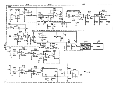
FIG. 3 is a preferred embodiment of a circuit
diagram fox enhancing stability during dimming of an
electrodeless HID lamp in accordance with the
teachings of the present invention;
FIG. 4 is a waveform of the light during dimming
for electrodeless HID lamp ~1 obtained through a
remote light sensor with photopic response during
dimming;
FIG. 5 is a waveform of the light from
electrodeless HID lamp ~2 measured in the same manner
using identical control circuit setting to those used
for the case shown in FIG. ~;
D-92-1-107 -~-- 3~Pv'fEtd'7C d~P~LICATIOhI
FIG. 6 are waveforms of the output voltage from
operational amplifiers OP2, OP3, OP1, and from the
light detector during the stabilizing region of lamp
#2 in FTG. 5 where light output fluctuates;
FIG. 7 are the waveforms of FTG. 6 provided on an
expanded time scale in order to show the cycle of
power control op-amp response during this period;
FIG. 8 are waveforms taken during the
equilibrated dim mode for lamp #1 of the steady state
dim made forward microwave power, reflected microwave
power, voltage supplied to the second stage of the
microwave amplifier, and lamp light emission;
FIG. 9 are tables containing photometric lamp
data taken at full power prior to dimming, after 25
seconds of dim mode operation, and after 12 minutes of
dim mode operation;
FIG. 10 is a graph illustrating instant light
level upon restoration of full power, for several
lamps, as a function of the time spent in the dim
mode;
FIGS. lla and llb are waveforms showing the
light rise from the dim level after six minutes of dim
operation fox lamps 90-170 and 91-070, respectively;
~1~.~~~1~
D-92-1-107 -9- P~TFN~' APPhICATI0~1
FIGS. 12a and 12b are waveforms showing light
rise at power up after 10 minutes of dim mode
operation on several occasions when the arc rooted
itself to the salt condensate for lamp 91-070; and
FIG. 13 are waveforms of the output of
operational amplifiers OP2, OP3, OP1 and the light
signal from OP4 for lamp 91-070 in dim mode.
BEST MODE FOR C~rItRYItdG Ot)T TFIE INVENTION
For a better understanding of the present
invention, together with other and further objects,
advantages and capabilities thereof, reference is made
to the following disclosure and appended claims in
connection with the above-described drawings.
Many factors affect arc discharge stability during
reduced power operation of a microwave excited
electrodeless metal halide lamp. These factors
originate from the characteristics of the discharge
itself as well as the characteristics of the microwave
power source. On the discharge side, the plasma
deionization time is a critical parameter which
profoundly affects stability and guenching probability
during reduced power operation. The deionization time
of the plasma is determined by the lamp fill
composition. On the microwave power source side,
critical parameters affecting stability include the
coupling structure, the matching network and the
method used to control the power level delivered to
2119'~1~
D-92-1-107 -1~- ~AT~t~t' Ap~x~xcATxAaa
tile lamp during dimming. A variety of workable
methods may be conceived of which control the source
power level duxing dimming. The most desirable of
these will include measurement of a signal which would
"inform" the control circuit when discharge quenching
is likely to occur in time for. corrective action to be
taken.
The present invention describes a method and
circuit for dimming an electrodeless microwave driven
high intensity discharge light source in a reliable
fashion to a reproducible level using a circuit means
which inhibits the lamp from ea~tinguishing during
unstable periods in the process. In the present
embodiment the lamp power source utilizes a three
stage microwave amplifier hawing isolated supplies and
an output power of 25 W at 915 ~dhz. During dimming,
the control circuitry described herein modifies the DC
voltage supplied to the second stage of the amplifier,
thereby affecting the amplifier's overall gain. This
then affects the power delivered to the lamp since a
constant power oscillator stage is input to the
amplifier. The DC voltage supplied to the amplifier's
second stage is modified by the circuit in response to
several °°informant signals", such as, the
instantaneous light output of the lamp, and the light
response to short repetitive pulses of full power
impressed on the lamp during dimming. As a result,
quenching is averted and stability is promoted during
dimming for a wide range of electrodeless lamps.
D-92-1-107 -11- PATExdT P.PPLICATION
Tn a preferred embodiment, forward power supplied
to the lamp is affected by three high gain negative
feedback circuit components. The first component
increases its output when 'the light response to the
power pulses falls below a reference level. The
second component increases its output when the rate of
light drop exceeds a reference rate. The third
component increases its output when the overall light
output falls below a reference level. The component
with the highest output at any given time determines
the power delivered to the lamp.
The lamp power source utilizes a three stage
microwave amplifier having isolated supplies and an
output power of 25 ~7 at X15 Mhz. During dimming, the
control circuitry described modifies the DG voltage
supplied to the second stage of the amplifier, thereby
affecting the amplifier's overall gain. This then
affects the power delivered to the lamp since a
constant power oscillator stage is input to the
amplifier. The DC voltage supplied to the amplifier's
second stage is modified by the circuit in response to
both the instantaneous light output of the lamp, and
to the light response to short repetitive pulses of
full power impressed on the lamp during dimming.
For a lamp operating at reduced power, the level of
light response to a pulse of full power will indicate
the ability of that lamp, at that time, to recover
elevated light output in response to elevated forward
power. Recovery becomes more difficult, and the
likelihood that the lamp will extinguish becomes
21i~~18
D-92-1-107 -12- P~TE~IT APPLICATION
greater, at times when the light does not respond
sufficiently to the power pulses.
Forward power supplied to 'the lamp is affected by
three high gain negative feedback circuit components.
The first component increases its output when the
light response to the power pulses falls below a
reference level. The second component increases its
output when the rate of light drop exceeds a reference
rate. The third component increases its output when
the overall light output falls below a reference
Level. The component with the highest output at any
given time determines the power delivered to the lamp.
The radio frequency power source may be any
conventional power source capable of providing a
selected frequency and power output. The preferred
radio frequency source should produce a radio
frequency power capable of inducing breakdown of the
enclosed lamp fill, and in particular a high frequency
source having a frequency from 10 Mhz. to 300 ~hz. is
preferred. The range of legally allowed frequency
beams may be smaller than the physically useful range,
so the frequency may be further limited to the
standard ISM frequencies such as from 902 Mhz. to 928
Mhz., or the ISM band centered at 2450 Mhz. The
preferred frequency used for the source was 915 Mhz.,
as this frequency is a legally permitted choice. A
suitable radio frequency source had an impedance of
about 50 ohrns. For reliable starting, the microwave
induced electric field inside the lamp capsule should
be greater i:han that needed to induce breakdown, which
D-92-1-107 -13- PATEPdT APPLIG~aTxOtd
for standard lamp fills is about 150 volts per
centimeter. The requirements for field breakdown may
be lowered substantially by using Penning gas
mixtures, or applying a bright ultraviolet light to
the lamp capsule. If necessary, a radio freguency
power source may be mounted on a heat sink near the
lamp capsule.
The capsule encloses a lamp fill that may
include various additional doping materials as is
known in the art. The lamp fill composition is chosen
to include at least one material that is vaporizable
and excitable to emission by the radio frequency
power. The lamp fill compositions useful here are in
general those familiar to arc discharge tubes, most of
which are felt to be applicable in the present design.
The preferred gas is a Penning mix of largely neon
with a small amount, less than 1%, argon, although
xenon, krypton, argon or pure neon may be used. the
lamp fill preferably includes a metallic compound,
such as a metallic salt. Scandium iodide is a
preferred metallic salt. ~ne such lamp fill
composition is 0.3 milligram of metallic mercury, 0.1
milligram of sodium-scandium iodide. Twenty torr of a
Psa~ning gas mix consisting of 0.0048% argon in neon
was used in a volume of about 0.03 cm3. Preferably,
the lamp capsule is made of 2 X 3 mm quartz tubing 10
mm long and generates 3000 lumens in the steady state.
Referring to the drawings, FIGS. la and 1b
demonstrate the light response resulting from power
pulses, with characteristics identical to those used
2~~~'~1~
D-92-1-107 -14- PATENT 1~PPZT~I~TI~N
in the present circuit, super:Lmposed on a recently
reduced background power level. In FIG. la, the
voltage supplied to the second stage of the microwave
amplifier is illustrated as a function of time. Sixty
microsecond wide pulses at a repetition rate of 1 Khz.
are superimposed on a recently reduced background
voltage. Each pulse elevates the forward microwave
power to its full output.
FIG. 1b illustrates the light response from the
lamp as a result of the second stage supply voltage
shown in FIG. la. The lamp in this case is purposely
allowed to extinguish in order to demonstrate the
decreasing light response level to the power pulses as
the lamp nears the extinguishing point, indicated by
the arrow at time T1 in FIG. 1b. The last light
response to a power pulse is indicated by the arrow at
level L1. This level corresponds to 6~ of the steady
state full power light output.
FIG. 2a shows a portion of the supply voltage and
light signal shown in FIGS. la and 1b, respectively,
displayed on an expanded time scale. The light
response in this time period is relatively large
indicating that the lamp is operating within a stable
region. Therefore, at that point in time, power
reduction may proceed without causing the lamp to
extinguish.
The region where light drops steeply just prior to
extinguishing is provided on an expanded time scale in
FIG. 2b. It is clear that the response level of the
light is drastically attenuated in this region.
~~~~~~8
D-92-i-107 -15- ~AT~~aT ~~~a,ICATIOra
In FTC. 2b the last detectable light response to a
60 microsecond wide pulse of full power occurs at 6~
of the steady state output of the lamp. The light
response level at this point is roughly 5 times less
than it was dust moments earlier when restoration of
the light through increasing the forward power level
was relatively easy indicating that the lamp was
operating within a stable regime.
The light response to elevated power pulses is a
valuable measure indicating when the discharge is
likely to extinguish. The instantaneous light
response level incorporates information relating to
the plasma conditions, the balance of ionization
production and loss, as well as the coupling
efficiency of power into the discharge at that time,
all of which directly affect the stability of the
plasma. When light response to the power pulse is
totally lost, it is unlikely that the discharge can be
recovered.
The source of microwave power is a 915 ~lhz.
oscillator with constant pawer output followed by a
Motorola three stage power amplifier. The second
stage of this amplifier has a DC supply isolated from
that of the first and third stages, allowing gain of
the overall amplifier to be controlled by the voltage
supplied to the second stage. The control circuit
developed herein provides this DC supply voltage for
the second stage of the amplifier. The DC supply
voltage for all three amplifier stages is nominally 15
volts.
D-92-1-107 -16- PATENT APPLICATION
Illustrated in FIG. 3, generally designated by
the number 10, is the presently preferred embodiment
of a circuit for enhancing stability during dimming of
an electrodeless discharge lamp 12. Circuit 10
employs a pulse generator 14, a light output monitor
16, a circuit 18 for generating a voltage proportional
to each increase in light output caused by each pulse
from pulse generator 14, and means for preventing
extinguishing of electrodeless discharge lamp 12
during dimming. In practice, the electrodeless '
discharge lamp is prevented from extinguishing during
dimming by one or more control circuits. In a
preferred embodiment, extinguishing of lamp 12 during
dimming is prevented by three control circuits 20, 22
and 24. Lamp power is adjusted in response to a
signal generated at the output of circuit 10 and
coupled to the second stage power amplifier portion of
a microwave oscillator and power amplifier 26.
In the preferred embodiment, pulse generator 14
includes a 555 timer chip IC1, resistors R6, R7 and
R8, and a timer capacitor C1. The output of timer
chip IC1 is connected t~ the gate terminal of a field
effect transistor (FET) T1 having a drain connected to
the junction of a resistor R8 and a diode D1. The
source of transistor T1 is connected to circuit
ground. As configured, pulses of full power are
provided to the lamp by the voltage pulses appearing
at terminal A. Preferably, the pulse repetition
frequency is 1 Khz and each pulse is 60 microseconds
wide. The 1 Khz pulse repetition frequency provides
D-92-1-107 -17- P,~TENT ~PPLxCATION
adequate time response to changing discharge
conditions while falling below the acoustic resonance
frAquencies for the lamps described. It also ensures
that the resultant light response will not be detected
by the human eye. As will be shown, an operational
amplifier OP1 operates on the change in light
intensity resulting from these pulses of full power.
To monitor lamp light, a fiber optic cable (not
shown) is placed approximately 8 centimeters away from
lamp 12. The other end of the fiber optic cable is
coupled to a photodiode PD1 constituting the input of
light output monitor 16. One suitable photodiode is
part na. 51336-5Rg manufactured by Hammamatzu. Light
output monitor 16 includes an operational amplifier
(op-amp) OP4, a transistor T2, a diode D2 and
resistors R9, R10 and R11. The output signal from
photodiode PD1 is connected to the non-inverting input
of op-amp OP4. The inverting and non-inserting inputs
of op-amp OP4 are coupled to circuit ground through
resistors R9 and R10, respectively. The output of op-
amp OP4 is connected to the gate of transistor T2.
Resister R11 Is connected between the inverting input
of OP4 and the junction of transistor T2 and diode D2.
after being amplified by op-amp OP4, the amplified
signal appearing at terminal 1 is utilized in three
major circuit functions to be described below.
Instead of directly measuring the change in light
signal on its rising portion during the power pulse,
the present invention detects the level of light
2119"71~
D-92-i-10'7 -18- PF~T~RIT P~PP~LICATxoN
decay, prior to the subsequent. pulse, with respect to
the peak light level during the pulse.
The ocatput of light output monitor 16 is connected
to the input of a circuit 18 which generates a voltage
proportional to each' increase in light output from
lamp 12 in response to each of the pulses generated by
pulse generator 14. These pulses are subsequently
applied to the lamp. Circuit 18 includes a peak
detector comprising capacitors C2 and C6, a transistor
T3 and resistors R12 and R13. In the present
embodiment, the peak detector portion of circuit 18 is
configured w9.th one end (terminal A) of capacitor C6
connected to the cathode of diode 01 in pulse
generator 14. The other end of capacitor C6 is
connected to the junction of resistor R12 and ttm gate
of transistor T3. The source of transistor T3 is
coupled to circuit ground through resistor R13. The
drain of transistor T3 is connected to the junction of
capacitor C2 and the cathode of diode D2 (terminal 2)
in light output monitor 16.
Capacitor C2 is connected through a resistor R15 to
the non-inverting input of an op-amp 0~5 and holds the
peak light output level generated by the power pulse.
The voltage held on peak detector capacitor C2 is
partially discharged through transistor T3 at the
beginning of each power pulse. This facilitates
storage of the true peak voltage at times when the
overall light signal is decreasing.
Tn the present configuration, a series combination
of a diode I53 and a resistor R14 is connected to the
2~1~~1~
D-92-1-107 -19- PATE' APPLICATION
inverting input of an op-amp 0P5. A resistor R16
couples the non-inverting input of op-amp OP5 to
circuit ground. A resistor R17 is connected between
the inverting input and the output of op-amp 0P5 which
is connected to the non-inverting input of an op-amp
OP6. The inverting input of op-amp OP6 is referenced
to ground through a resistor R18. A resistor R19 is
connected between the inverting input and the output
of op-amp OP6. The output of op-amp OP6 is coupled
through a resistor R22 to the non-inverting input of
an op-amp OP7 which is coupled to circuit ground
through the parallel combination of a resistor R21 and
a capacitor C3. The inverting input of op-amp OP7 is
referenced to ground through a resistor R20. A
resistor R23 is connected between the inverting input
and the output of op-amp OP7 (terminal 3).
In operation, op-amp OPT of light output monitor 16
provides input to op-amp OP5 which is configured as a
unity gain differential amplifier. The output of op-
amp OP5 represents the difference developed between
the real time light signal and the voltage held on the
peak detector capacitor C2. The difference signal is
then amplified by op-amp OP6. The output of op-amp
0P6 is a signal which increases in amplitude as the
light from the lamp decreases after the power pulse.
The output of op-amp OP6 is then fed to the non-
inverting input of OP7 which forms a differential
amplifier having a ground reference attached to the
inverting input through resistor R20. Capacitor C3 at
the non-inverting input of op-amp OP7 holds a voltage
2~1971~
~-92-1-107 -20- PAT~~T APP~zcATZ~~
proportional to the peak output of op-amp OP6
occurring after each power pLdlse. As a result, the
output of op-amp OP7 (terminal 3) is a DC voltage
proportional to the change in light level resulting
from the power pulse. More precisely, the output
signal is a DC voltage proportional to the light level
decay after the pulse. This provides an accurate
measure of the light response to the power pulse
provided that the light response level does not change
faster than capacitor C3 can charge or discharge. For
this reason, capacitor C3 is chosen as small as
possible while still maintaining a relatively constant
output at op-amp OP7 between two successive power
pulses.
The embodiment in FIG. 3. includes a first
control circuit 20 comprising an op-amp OPl having an
inverting input coupled through a resistor R24 to the
output of op-amp OP7 (terminal 3) in circuit 1~. A
reference voltage is established at the non-inverting
input of op-amp OP1 by means of a transistor T4, a
capacitor C4, a variable resistor R1, a diode D4 and
resistors R25 and R27. In the present configuration,
capacitor C4 is connected across the drain and source
of transistor T4. The junction of diode D4, capacitor
C4 and the source of transistor T4 is coupled through
resistor R25 to the non-inverting input of op-amp OP1
which is coupled through resistor R27 to ground. The
anode of diode D4 is connected to the wiper terminal
of variable resistor R1. A resistor R26 is connected
4
~ ~. ~. J °~'. 8
D-92-1-107 -21- PATEi~IT APPLICATION
between the inverting input and the output of op-amp
OP1.
The output of op-amp OP1 is coupled through a
pair of diodes D5 arid D6 to the gate of a transistor
T5. The junction of diodes D5 and D6 (terminal 7) is
coupled to ground through a resistor R28. The
junction of the cathode of diode D6 and the gate of
transistor T5 is coupled to ground through a resistor
R29. The source of transistor T5 is coupled through a
diode D7 to a common junction terminal
In operation, op-amp OP1 increases its output
voltage when the light response to the power pulses,
as output from op-amp OP7, falls below the reference
value found on the non-inverting input of op-amp OP1.
Op-amp OP1 increases power to the lamp when its output
voltage exceeds that of any other power control leg
connected to the gate of a transistor T5 (junction
terminal ~). The reference value for op-amp OP1 is
initially high and ramps down as capacitor 04
discharges to a value determined by variable resistor
R1. At its lowest level the reference voltage is set
to about 0.2 - 0.3 Volts. The exact value is not
critical but if it is set too high (several volts or
more) it may be greater than the equilibrated dim
level light response, thereby causing the lamp to
flash unnecessarily or cycle in light level when in
the dim mode.
A second control circuit 22, having an input
(term.inal 1) connected to the output of light output
monitor 16, includes operational amplifiers OP9, OP9
2119~1~
D-92-1-107 -22- PATEWT APPZ1CATI0~
and OP2. In the present conf:lguration, the inverting
input of op-amp OP8 is aonneci~ed to the junction of a
pair of resistors R32 and R33. The other_ side of
resistor R32 is connected to the wiper terminal of a
variable resistor R3. The output of op-amp OF8 is
coupled through a resistor R35 to the inverting input
of op-amp OP9. Similarly, the output of op-amp OP9 is
coupled through a resistor R37 to the inverting input
of op-amp OP2. The output of op-amp OP2 is connected
to the gate of a transistor T6 having an output
(terminal 5) coupled through a diode D10 to a common
terminal junction 8. Resistors R34, R36, and R39 are
connected between the inverting input and the output
of op-amps OPB, OP9 and OP2, respectively. The non-
inverting input of op-amp OP2 is coupled through a
resistor R40 to ground and through a resistor R38 to
peak detector capacitor C2 (terminal 2) of circuit 18.
In operation, second control circuit 22 functions
as a light reduction rate limner. When the light
signal level at terminal 1 added to the voltage set on
variable resistor R3, falls below the voltage held on
capacitor C2 of circuit 18 (at terminal 2), op-amp OP2
swings its output high elevating the power applied to
the lamp. This occurs when the light signal from op-
amp OP4 in light output monitor 16 drops at a rate
faster than the rate voltage decays on Capacitor C2 as
a result of discharge through transistor T3 of circuit
18.
Op-amp OP8 in circuit 22 functions as a summing
amplifier and op-amp OP9 is an inverter placing a
~1~J"d18
D-~2-1-l07 -2a- P,~TEraT APr~.acATZOra
positive voltage sum on the inverting input of op-amp
OP2. When the light signal at terminal 1 remains
above the voltage on capacitor C2 by a voltage equal
to one diode drop plus the voltage set on resistor R3,
op-amp OP2 swings low and returns power control to
another leg in the circuit.
Preferably, the voltage set at variable resistor R3
is approximately 0.27 volts. If this setting is set
too low the lamp may not dim properly since the light
drops after each pulse of power might not be
permitted. If the setting is too high the lamp may
extinguish during dimming.
A third control circuit 24, having an input
(terminal 1j connected to the output of light output
monitor 16, includes operational amplifiers OP10, OP11
and OP3. As presently configured, the inverting input
of og-amp OP10 is connected to the junction of a pair
of resistors R41 and R42. The other side of resistor
R41 is connected to the wiper terminal of a variable
resistor R4. The output of op-amp OP10 is coupled
through a resistor R44 to the inverting ingot of op-
amp OP11. The output of op-amp OP11 is connected to
the gate of a transistor T7 which has an output source
terminal coupled through a pair of diodes D12 and D13
to the non-inverting ingot of op-amp OP3. The
function of diodes D12 and D13 is conned to the
parallel combination of a capacitor C5 and a resistor
R46. The non-inverting input of og-amp OP3 is coupled
to ground through a resistor R4~. The inverting input
~0 of op-amp OP3 is coupled through a resistor R50 to the
21~~~~8
D-92-1-107 -24- PATENT APPLICATION
output of light autput monitor 16 at terminal 1. A
variable resister R5 has a wiper terminal coupled
through a series combination of a resistor R47 and a
diode D14 to the non-inverting input of ap-amp OP3.
Resistors R43, R45, and R49 are connected between the
inverting input and the output: of op-amps OP10, OP11
and OP3, respectively. The output of op-amp OP3
(terminal 6) is coupled through a diode D11 to common
terminal junction 8.
In operation, op-amp OP3 functions as an absolute
valued light level clamp and increases power to the
lamp if the light output signal from op-amp OP4 falls
below the reference voltage at the non-inverting
input. The reference voltage is initially high prior
to dimming, when switches S1 and S2 are closed, since
the light signal from op-amp OP4 is supplied to the
inverting input of the summing amplifier OP10 of third
control circuit 24. As the light level decreases and
the voltage on capacitor C5 discharges, the reference
voltage drops to a clamped level set by variable
resistor R5.
Variable resister R4 at terminal 7 is placed in the
circuit to add a small quantity to the light signal
detected by the adjacent op-amp OP10, at times when
op-amp OP1 of first control circuit 20 sings high.
This elevates the reference voltage at op-amp OP3 to a
selectable value above the light signal level at the
time the instability occurred. Elevating the
reference control level of op°amp OP3 in this manner
gives the lamp more time to come into equilibrium at a
221~~1~.~
D-92-1-107 -25- PATE1~T APPLICATION
particular power level. This can sometimes reduce the
severity of flickering instab~.lities by allowing the
light to decrease gradually from an elevated level as
capacitor C5 discharges. As equilibrium conditions
establish at a particular power level, the light
response to the power pulse wLll typically increase in
amplitude. As this occurs, op-amp OP1 swings low and
power control is typically provided thereafter by op-
amp OP3.
The output of op-amp OP1 in control circuit 20
swings high at times when the light response to a
power pulse is insufficient as determined by the
reference level at its non-inverting input. As
increased power is supplied to the lamp, increased
conductivity is established. At a certain point, the
light response to the power pulses will again exceed
the reference level causing the output of op-amp OP1
to swing low. Immediately after this occurs, the
output of op-amp OP2 in second control circuit 22
provides power to the lamp in order to limit the light
drop rate. When the light level falls to the
reference value on op-amp OP3 in third control circuit
24, op-amp OP-~ controls the power to the lamp. If
conditions for lamp stability are unfavorable at this
time the light response to the power pulse will again
be insufficient thereby elevating the output of op-amp
OP1 high once again.
During these stabilizing periods the lamp will
flash or cycle its light output briefly. Eventually,
as the lamp comes into equilibrium for that range of
~~1~~~~
D-92-1-107 -26- PATRNT APPLICATION
power, matching conditions will typically improve,
light response to the power pulses will increase and
future power control while in the dim mode will be
carried out by op-amp nP3.
The output from control circuits 20, 22 and 24 axe
connected to common terminal junction 8 which serves
as the input terminal to a pair of follower
transistors T8 and T9. In this portion of circuit 10,
a diode D8 is connected in series with the parallel
combination of a capacitor C7 and switch S1. In the
present configuration, a resistor R30 couples the gate
of transistor T8 to ground. The base of transistor T9
is coupled to ground through a resistor R31. The
emitter of transistor T9 is connected to the second
stage of a three stage 915 Mhz. power amplifier 26.
The wiper terminal of a variable resistor R2 is
coupled through a diode D9 to the gate of transistor
T8. Variable resistor R2 prevents the voltage on the
gate of the follower transistor T8 from dropping below
a particular level. In this manner, microwave power
may never be fully cut off at any point during dim
mode operation.
Light from electrodeless discharge lamp 12 is
monitored by a fiber optic cable coupled to photodiode
PDl located remotely along with the rest of the
control circuitry. Dimming is initiated by opening a
pair of switches S1 and S2, placing circuit 10 into
control. Voltage supplied to the second stage of
power amplifier 26 is reduced immediately due to the
voltage drops across the diodes and follower
2~.1~~11~
D-92-1-107 -27- PATENT APPLTCATION
transistors at the outputs of power control circuits
20, 22 and 24. Oscillator and power amplifier 26 is
impedance matched to lamp 12.
FIG. 4 shows the light from electrodeless HID lamp
#1, measured with an additional detector during
dimming. The signal is obtained through a remote
light sensor with photopic response. Switches S1 and
S2 in FIG. 3 are opened at time T1. This lamp
exhibits rapid stable dimming properties.
FIG. 5 shows the light from electrodeless HID lamp
#2, measured in the same manner using identical
control circuit setting to those used for the case
shown in FIG. 4. HID lamp #2 is less tolerant of
rapid dimming and requires a period of stabilization
indicated by the light fluctuations.
FIGS. 4 and 5 demonstrate the ability of the
control circuit to operate, without readjustment, on a
range of lamps with properties differing to a extent
larger than the expected manufacturing tolerances.
Lamp #1 and lamp #2 contain vastly different fills.
Lamp #1 contains over three times the mercury dose of
lamp #2. The lamps are also mounted in separate
coupling structures utilizing different matching
networDcs .
FIG. 6 provides measurements of the output voltages
from operational amplifiers OP2, OP3, OP1, and from
the light detector during the stabilizing region of
lamp #2 in FIG. 5. These waveforms are provided on an
expanded time scale in FIG. 7 in order to show the
211~~18
D-92-1-107 -28- PATENT APPLICATION
cycle of power control op-amp response during this
period.
PIG. 8 provides measurements during the
equilibrated dim mode for lamp #1 of steady state dim
mode forward microwave power, reflected microwave
power, voltage supplied to the second stage of the
microwave amplifier, and lamp light emission. Forward
and reflected microwave power are measured using
Hewlett Packard model 423H crystal detectors attached
to a dual directional coupler. These detectors owtput
a negative voltage proportional to the microwave
power. Therefore higher power levels on FIG. 8 are
read in the negative direction, as indicted by the
scale to the right of the power curves. At this
stage, power control is provided by op-amp OP3 after
each pulse.
The fill for lamp #1 is as follows: 0.95 mg Hg,
0.13 mg NaScI4 with i.6 . 1 molar ratio, and 20.2 Torr
Ne-Ar Penning mix as a buffer gas. Lamp #1 was given
the numerical designation 91-070 at the time of
filling. The fill for lamp #2 is the following: 0.31
mg Hg, 0.11 mg NaScI4 with 1.6 . 1 molar ratio, and
20.2 Torr Ne-Ar Penning mix. Lamp #2 was given the
numerical designation 91-110 at the time of filling.
The color properties of the discharge change during
dimming. Typically for the lamps observed, color
temperature will shift to lower values immediately
after power reduction and will then slowly shift to
higher values as the wall temperature cools and
mercury emission dominates. FIG. 9 are tables
2~.~~~11~
T1-92-1-107 -29- P~,TE~1T I~PPLICA7~zoN
containing photometric lamp data for lamp 90-170 taken
at full power prior to dimming, after 25 seconds of
dim mode operation, and after 12 minutes of dim mode
operation. Tamp 90-170 contains a fill identical to
lamp #2 discussed earlier.
the lamp may be brought back to full power
operation at any moment after dimming is initiated.
Full power restoration is accomplished by closing
switches Sl and S2 of FIG. 3. this action initiates a
rapid restoration to full light output. As mentioned
previously the light rise time depends upon both the
length of time spent by the lamp in the dim mode and
upon the fill composition.
FIG. 10 shows the instant light level attained by
several lamps as a franction of time spent in the dim
mode. ~'he dim mode light level for these measurements
was 10~ of the steady state light level. Instant
light, in this case, is defined to be the light level
attained in the first 200 milliseconds after full
power restoration. The instant light level attained
is plotted relative to the lamp's steady state light
level. '~h~ decreasing level of instant light with
increasing time spent in the dim mode is a result of
the arc tube wall temperature decrease with time. The
wall temperature decrease reduces the vapor pressure
of the volatile components and thereby reduces instant
light capabilities over time.
In laboratory conditions the rise times from the
dim mode approach the cald start rise time (after arc
constriction) after approscimately five minutes of
~-92-1-l07 -~o- P,~1TEA1'1' APPLICATIOid
operation in the dim mode. FIGS. lla and llb show the
light rise from the dim level after six minutes of dim
operation for lamps 90°170 and 91-070, respectively.
Lamp 91-070 exhibits a longer rise time perhaps as a
result of its increased mercury dose. Measurements
were made using a detector with photopic response.
Occasionally upon restoration of full power, lamps
have been observed to flash up rapidly to full light
output even after extended periods of operation in the
dim mode. Light has been observed to reach 85~ of
steady state output within a fraction of a second and
continue to increase steadily, sometimes above the
steady state level, as the arc capsule temperature
rises. This occurs when the arc roots itself to the
salt condensate at power-up thereby rapidly vaporizing
it. Several examples of light output during this
occurrence with lamp 91-070 are provided in FIGS. 12a
and 12b.
The circuit illustrated in FIG. 3 is presented as a
proof of principle design. It is in no way optimized
and many improvements could be made. Understandably,
those more skilled in the art of circuit design could
no doubt improve the methodology in the circuit used
to preferably accomplish its three main functions,
those of operational amplifiers OP1, OP2, and OP3.
Gated digital sample and hold circuits could be
used to detect unambiguously the level of light
response on the rising portion during each power
pulse. The response time of the circuit to changes in
light response could be greatly improved if such
D-92-1-107 -31- PATENT APPbICATION
techniques were used. In the current design a number
of pulses pass before op-amp OP1 is able to respond to
rapidly changing conditions. This is a result of the
discharging time of capacitor C3 attached to the non-
inverting input of op-amp OP7. If light from the lamp
should suddenly fail to respond to a power pulse, time
must elapse while capacitor C3 discharges and the
output of op-amp OP7 drops below the reference voltage
at op-amp OP1, before op-amp OP1 responds by elevating
its output high thereby increasing power to the lamp.
In order to illustrate this response time, a pen
was passed in front of the fiber optic cable
monitoring light emission while the lamp was in its
dim state. While light is blocked by the pen the
circuit detects zero light, and therefore zero light
response to the power pulses, and thus should elevate
power through op-amp 0P1. The time required for this
to occur is illustrated in FIG. 13 along with the
response of the other two op-amps OP2 and OP3.
When the light is blocked op-amp OP3 immediately
swings steadily high sensing an overall light level
below its reference point. Operational amplifier OP1
does not begin to respond until 10 milliseconds later
whewcapacitor C3 has sufficiently discharged. By the
time the pen passes from view of the fiber optic
cable, light has increased above the reference point
at op-amp OP3 and its output swings low. This is
followed by op-amp OP1 swinging low as sufficient
light response to power pulses is again detected.
3fl Overall light from the lamp now drops. The rate of
21~~~1~
D-92-1-107 -32- P~TE~T APP~IOATION
the drop is limited by the output of op-amp OP2. The
action of op-amp OP2 in these instances is vital to
the avoidance of quenching. 6~hen the overall light
decreases to the control leve:L of op-amp OP3, its
output thereafter controls power to the lamp. The
response time of the present circuit does not appear
to cause any performance diff:Lculties, but if it were
reduced the circuit would be capable of operating on
an even wider range of lamp variations.
One subtlety exists in the circuit for its
successful operation. The power level generated by
the power pulses must be somewhat higher than the
power level produced by a full 15V swing of any of the
power control op-amps. This is required so that
sufficient light response to pulses is still be
detected even at times when any one power control op-
amp has swung to its full output. If this were not
the case, op-amp OPl could latch up at the full power
level. The diodes and follower transistors at the
outputs of operational amplifiers OPl, OP2, and OP3
develop a sufficient voltage drop prior to the pulse
infection terminal A on the gate of transistor T~ in
order to avoid this problem. The drawback to this is
that something less than full supply output power is
available for recovery of an extinguishing discharge.
If the power supply could be pulsed above the steady
state power level, then at least steady state power
levels could be available for recovery periods. This
modification could only enhance dimming performance.
D-92-1-107 -33- PATENT APPbICATyON
Finally, the efficiency of the dimming process
could be greatly improved by using a constant gain
amplifier and modifying the oscillator output power in
response to the control circuit output voltage.
Presently the final follower transistor T9 dissipates
significant power and is therefore mounted on the heat
sink provided for the microwave amplifier.
During dimming, the rate of power decay is in part
controlled by RC time constant decays in the reference
voltages placed on operational amplifiers OP1, OP2,
and OP3. It may be feasible to make the dimming rate
a function of the rate of change in light response to
the power pulses. This may require referencing the
light response level to the overall light level in a
continuous fashion. But in any case, the idea would
be to have a power reduction scheme which reduced
power at times when a large light response is
detected, at a rate which decreased or stopped when
the level of light response decreased rapidly, thereby
allowing the lamp to reach an equilibrium condition
for that level of power. As this equilibrium
condition establishes, the light response to power
pulses will again increase in amplitude indicating
that further power reduction may proceed. This could
be sensed by the circuit and initiate further power
reduction. This type of scheme may enable lamps to be
dimmed over time to extremely low light levels but the
dimming rate would vary from lamp to lamp.
If stable reliable dimming to extremely low light
levels is achievable utilizing such a scheme, the lamp
D-92-1-io7 -34- p~~~R~ App~IC~TaoR
could be dimmed to the point where it has cooled
sufficiently to turn power off completely, and restart
immediately thereafter, as a cold lamp, if desired.
Assuming the cold start light rise time for the lamp
is sufficiently rapid, this type of system could find
applications in automotive forward lighting. In such
a system rapid restoration to full light at any moment
it is desired would be achievable thereby
circumventing the hot restart problem fox
electrodeless headlamps.
As a specific example but in no way to be construed
as a limitation, the following components are
appropriate to an embodiment of the present
disclosure, as illustrated by FIC. 3a
Item Description Value of Part
No.
C6 Capacitor 6$0 PFD
C3 Capacitor 0.05MFD
C1 Capacitor O.1MFD
C2,C5,C7 Capacitors 1 MFD
C4 Capacitor 10 MFD
R1 Variable resistor 1 Mohm
R2,R3 Variable resistor 10 Kohm
R4,R5 Variable resistor 2 Kohm
R13 Resistor 22 ohm
R$ Resistor 220 ohm
R11 Resistor 2~0 ohm
R7 Resistor $20 ohm
R18 Resistor 1 Kohm
D-92-1-i07 -35- ~~TERT ~ppLac~TaDR
R24-R25,R37-R38, Resistors 1.3 Kohm
R47,R50
R9-R10 Resistors 1.8 Kohm
R28 Resistor 2 Kohm
R12 Resistor 2.7 Kohm
R31-R36,R44-R45 Resistors 10 Kohm
R6 Resistor 12 Kohm
R19 Resistor 22 Kohm
R26-R27 Resistors 39 Kohm
R29-R30 Resistors 100 Kohm
R14-R17,R20-R23, Resistors 150 Kohm
R41-R43
R48-R49 Resistors 820 Kohm
R39-R40 Resistors 1 Rohm
R46 Resistor 2.7 Mohm
T1-T8 FET Transistors RSS 98
T9 Transistor ECO 152
Di-D14 Diodes ECO 125
OPi-OR11 Op-amps LF353
S1-S2 Switches DPST
PD1 Photodiode 51336-5BQ
There has thus been shown and described a power
control method and an apparatus for providing
stability during dimming of an electrodeless high
intensity metal halide discharge lamp through remote
optical sensing of lamp light output coupled with
power control circuitry which first, modifies power
delivered to the lamp based on the light response to
D-92-1-107 --36- PAT~Rd'i' A~PLIC~TION
well defined pulses of power :ln the microwave source
output, second, increases powE:r delivered to the lamp
when the rate of light drop exceeds a predetermined
rate, and third, controls the power delivered to the
lamp based on the overall light emission intensity.
The aim in developing the present control means is to
provide a power control method for electrodeless HID
lamp dimming which provides stable dimming regardless
of the initial conditions of the discharge, as well as
to provide a dimming means more forgiving of light-
source-system manufacturing tolerances than is
presently avaflable using absolute light intensity
control alone when source output power is limited.
While there have been shown and described what
are at present considered to be the preferred
embodiments of the invention, it will be apparent to
those s~Cilled in the art that various changes and
modifications can be made herein without departing
from the scope of the invention. Therefore, the aim
in the appended claims is to cover all such changes
and modifications as fall within the true spirit and
scope of the invention. The matter set forth in the
foregoing description and accompanying drawings is
offered by way of illustration only and not as a
limitation. The actual scope of the invention is
intended to be defined in the following claims when
viewed in their proper perspective based on the prior
art.