Note: Descriptions are shown in the official language in which they were submitted.
CA 021200~7 1998-04-14
TIME DIVISION DUPLEX TRANSCEIVER
The present invention relates to a time
division duplex transceiver for alternately transmit-
ting and receiving a signal having the same frequency.
In conventional two-way radio communication
systems, such as portable telephones, frequency-divi-
sion duplex (FDD) is often used. According to FDD, the
radio communication system transmits a signal having a
first frequency and receives a signal having a second
frequency which is different from the first frequency.
However, in recent years, since time-division multi-
plexing can be easily achieved with respect to a digi-
tal signal, time-division duplex ( TDD ) has attracted
considerable attention. According to TDD, the radio
communication system alternately transmits and receives
a signal having the same frequency. Compared with FDD,
TDD iS advantageous, for example, in that it is easy to
allocate a frequency to each of a transmitting signal
and receiving signal, and that transmitting and receiv-
ing efficiencies can be made substantially equal.
In a time-division duplex transceiver, a
transmitting frequency is identical with a receiving
frequency. When a signal having the transmitting
frequency is generated within the transceiver during
the receiving operation of the transceiver, the signal
is likely to enter the receiving section of the trans-
ceiver. This interferes with the receiving operation
of the transceiver and deteriorates the receiving
, ~.
, :
, . ~
CA 021200~7 1998-04-14
~_ -- 2
performance. Thus, during the receiving operation of
the transceiver, it is necessary to completely termi-
nate the generation of the signal having the transmit-
ting frequency.
Furthermore, in cases where the transceiver
is of a superheterodyne configuration and uses a local
signal for frequency conversion in both of the trans-
mitting and receiving sections of the transceiver, a
la transmitting intermediate frequency is identical with a
receiving intermediate frequency. Thus, the above-
described problem of deterioration in the receiving
performance also arises when a signal having the trans-
mitting intermediate frequency is generated during the
receiving operation of the transceiver. In such a
transceiver, therefore, it is necessary to completely
- terminate the generation of the signal having the
transmitting intermediate frequency.
The generation of the transmitting signal can
be prevented by terminating the operation of a trans-
mitting local oscillator during the receiving operation
of the transceiver. However, it is practically impos-
sible to terminate the operation of the transmitting
local oscillator during the receiving operation of the
transceiver. This is because the local oscillator
cannot be turned on and off rapidly enough to coincide
with the high-speed alternation between transmission
and reception in the transceiver. Thus, a common way
of terminating the generation of the transmitting
signal is as follows: During the receiving operation
of the transceiver, with the transmitting local oscil-
lator kept in operation, the signal line for the local
CA 021200~7 1998-04-14
_ -- 3
signal or transmitting signal is electrically cut off,
or a circuit which allows these signals to pass there-
through is disconnected from its power source, there~y
terminating the generation of the transmitting signal.
In this case, however, when the isolation of the elec-
trically-disconnected circuit is not sufficient, the
generation of the transmitting signal cannot be com-
pletely terminated during the receiving operation of
the transceiver. When the transmitting signal is
1~ generated during the receiving operation of the trans-
ceiver, the transmitting signal is likely to enter the
receiving section of the transceiver. This interferes
with the receiving operation of the transceiver, there-
by deteriorating the receiving performance.
To prevent such deterioration in the receiv-
ing performance, there has been developed a time-divi-
sion transceiver including a local oscillator for
producing a frequency of an integral multiple of a
transmitting frequency which also includes a divider.
For example, this type of transceiver is disclosed in
Japanese Laid-Open Patent Publication No. 4-240924. In
this transceiver, the output of the local oscillator is
divided so as to obtain a signal having a transmitting
frequency. During the receiving operation of the
transceiver, with the local oscillator kept in opera-
tion, the divider is electrically disconnected from the
local oscillator, thereby preventing the generation of
the signal having the transmitting frequency.
In such a time-division transceiver, however,
the local signal from the local oscillator is required
to have a frequency equal to or higher than twice that
CA 021200~7 1998-04-14
-- 4
of the transmitting signal. When the transmitting
signal has a higher frequency, it becomes more diffi-
cult to produce a stable local oscillator. This results
in the cost of producing the transceiver being high.
The transceiver of this invention for trans-
mitting and receiving a signal having the same frequen-
cy according to a time-division includes: a local
oscillator for generating a local signal having a first
frequency; a frequency converter for converting the
local signal into a carrier signal; a modulator for
modulating the carrier signal by using a transmitting
baseband signal so as to generate a transmitting signal
having a second frequency; and a receiving section for
receiving a receiving signal having the second frequen-
cy which is the same as that of the transmitting sig-
nal, wherein the frequency converter includes a frac-
tional frequency converter for converting a signal
having an input frequency into a signal having an
output frequency, the output frequency being n2/n1
times the input frequency, where n1 is an integer
greater than 2, n2 is an integer greater than 1, n1 and
n2 being relatively prime, whereby the second frequency
of the transmitting signal is not any integral multiple
of the first frequency of the local signal. The
transceiver further comprises a control means for
selectively terminating operation of the frequency
converter, wherein, in the receiving operation of the
transceiver, the operation of the frequency converter
is terminated.
In one embodiment of the invention, the
fractional frequency converter includes at least one
divider and at least one multiplier which are connected
in series.
CA 021200~7 1998-04-14
__
-- 5
In another embodiment of the invention, the
termination of the operation of the frequency converter
is accomplished by the control means by terminating
operation of the divider in the receiving operation of
the transceiver.
In another embodiment of the invention, the
termination of the operation of the divider is
accomplished by the control means by interrupting a
signal input to the divider in the receiving operation
of the transceiver.
In another embodiment of the invention, the
local signal is supplied to the receiving section, and
the receiving section performs at least one of frequen-
cy conversion and detection of the receiving signal by
using the local signal.
In another aspect of the present invention,
a transceiver for transmitting and receiving a signal
having the same frequency according to a time-division
includes: a first local oscillator for generating a
first local signal having a first frequency; a first
frequency converter for converting the first local
signal into a carrier signal; a modulator for modulat-
ing the carrier signal by using a transmitting baseband
signal so as to generate a modulated signal having a
second frequency; a second local oscillator for genera-
ting a second local signal having a third frequency; a
second frequency converter for converting the modulated
signal into a transmitting signal having a fourth
frequency in accordance with the third frequency of the
second local signal; a third frequency converter for
converting a receiving signal having the fourth fre-
quency which is the same as that of the transmitting
CA 021200~7 1998-04-14
-- 6
signal into an intermediate-frequency signal in accord-
ance with the third frequency of the second local
signal; and a receiving section for receiving the
intermediate-frequency signal, wherein the first fre-
quency converter includes a fractional frequency con-
verter for converting a signal having an input frequen-
cy into a signal having an output frequency, the output
frequency being n2/n1 times the input frequency, where
n1 is an integer greater than 2, n2 is an integer
greater than 1, n1 and n2 being relatively prime,
whereby the second frequency of the moudlated signal is
not any integral multiple of the first frequency of the
first local signal. The transceiver further comprises
a control means for selectively terminating operation
of the frequency converter, wherein, in the receiving
operation of the transceiver, the operation of the
first frequency converter is terminated.
In one embodiment of the invention, the
fractional frequency converter includes at least one
divider and at least one multiplier which are connected
in series.
In another embodiment of the invention, the
termination of the operation of the first frequency
converter is accomplished by the control means by ter-
minating the operation of the divider in the receivingoperation of the transceiver.
In another embodiment of the invention' the
termination of the operation o~ the divider is accom-
plished by the control means by interrupting a signal
input to the divider in the receiving operation of the
transceiver.
,
CA 021200S7 1998-04-14
In another embodiment of the invention, the
first local signal is supplied to the receiving sec-
tion, and the receiving section performs at least oneof frequency conversion and detection of the intermedi-
ate-frequency signal by using the first local signal.
The time-division duplex transceiver having
the configuration mentioned above does not require a
local signal having a higher frequency. Further,
according to the time-division duplex transceiver, the
local signal and its harmonic components do not provide
any interference with the receiving operation of the
transceiver. This is because the local signal and the
harmonic components thereof have frequencies which
cannot be close to a receiving frequency.
Thus, the invention described herein makes
possible the advantage of providing a time-division
duplex transceiver in which a signal having a transmit-
ting frequency can be prevented from interfering with
the receiving operation of the transceiver without
requiring a local oscillator capable of generating a
frequency higher than the transmitting frequency.
This and other advantages of the present
invention will become apparent to those skilled in the
art upon reading and understanding the following de-
tailed description with reference to the accompanyingfigures, in which:
CA 021200~7 1998-04-14
Figure 1 is a bloc~ diagram showing a config-
uration for a transceiver according to the invention.
Figure 2 is a block diagram showing a config-
uration for a waveform-shaping filter in the transceiv-
er of Figure 1.
Figure 3 is a block diagram showing a config-
uration for a receiving section in the transceiver of
Figure 1.
Figure 4 is a block diagram showing an exem-
plary configuration for a frequency converter in thetransceiver of Figure 1.
Figure 5 is a block diagram showing another
exemplary configuration for the frequency converter in
the transceiver of Figure 1.
Figure 6 is a block diagram showing another
configuration for a transceiver according to the inven-
tion.
Figure 7 is a bloc~ diagram showing a config-
uration for a frequency converter in the transceiver of
Figure 6.
Figure 8 is a block diagram showing an exem-
plary configuration for a receiving section in the
transceiver of Figure 6.
CA 021200~7 1998-04-14
'_ _ 9
Figure 9 is a block diagram showing another
exemplary configuration for the receiving section in
the transceiver of Figure 6.
The invention will be described in detail
with reference to the accompanying drawings.
Example 1
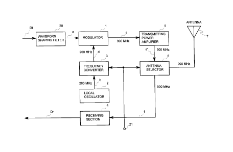
Figure 1 shows a configuration for a time-
division duplex transceiver of a first example accord-
ing to the present invention. The transceiver includes
a modulator 1, a local oscillator 2, a frequency con-
verter 3, a receiving section 4, a transmitting poweramplifier 5, an antenna selector 6, an antenna 7 and a
waveform-shaping filter 20.
Hereinafter, the transmitting operation of
the transceiver is described.
Transmitting data Dt is input to the waveform
shaping filter 20. The waveform-shaping filter 20
outputs a transmitting baseband signal a in accordance
with the transmitting data Dt. For example, the wave-
form-shaping filter 20 includes a digital filter 81 and
a D/A converter 82, as is shown in Figure 2.
The local oscillator 2 generates a local
signal b during both the transmitting and receiving
operations of the transceiver. The local signal b is
supplied to the frequency converter 3. The frequency
converter 3 frequency-converts the signal b into a
CA 021200S7 1998-04-14
-- 10 --
carrier signal d. As will be described in detail
later, the frequency converter 3 generates the carrier
signal d only during the transmitting operation of the
transceiver. In the receiving operation of the trans-
ceiver, the generation of the carrier signal d iscompletely terminated.
The modulator 1 modulates the carrier signal
d by the use of the baseband signal a so as to output a
modulated signal e. The modulated signal e is then
amplified by the transmitting power amplifier 5, re-
sulting in a transmitting signal e'.
Through a terminal 21, a control signal is
input to the antenna selector 6 and the frequency
converter 3. The control signal is used to switch the
transmitting operation and the receiving operation of
the transceiver. In the transmitting operation of the
transceiver, the antenna selector 6 is electrically-
connected to the transmitting power amplifier 5, sothat the transmitting signal e' passes through the
antenna selector 6 and is transmitted from the trans-
ceiver through the antenna 7. In the receiving opera-
tion of the transceiver, the antenna selector 6 is
connected to the receiving section 4. A signal input
to the antenna 7 is supplied to the antenna selector 6
which then outputs a receiving signal f. In the time-
division duplex transceiver, the receiving signal f
has the same frequency as that of the transmitting
signal e'. The receiving signal f is supplied to the
receiving section 4.
CA 021200~7 1998-04-14
The receiving section 4 outputs receiving
data Dr. The receiving data Dr is obtained by subject-
ing the receiving signal f to detecting and decoding
processes.
Figure 3 shows a configuration for the re-
ceiving section 4. In this example, the receiving
section 4 is of a superheterodyne configuration and
includes a local oscillator 41, a mixer 42, a detector
43, a clock recovery circuit 44 and a decoder 45.
The local oscillator 41 generates a local
signal. The local signal from the local oscillator 41
is supplied to the mixer 42. The mixer 42 mixes the
receiving signal f with the local signal from the local
oscillator 41. Then, the output of the mixer 42 is
subjected to detection, clock recovery, and decoding in
that order by means of the detector 43, the clock
recovery circuit 44 and the decoder 45, respectively,
resulting in the receiving data Dr.
Alternatively, the local signal b from the
local oscillator 2, instead of the local signal from
the local oscillator 41,may be supplied to the mixer
42.
Next, the frequency converter 3 will be
descri~ed in detail.
Figure 4 shows a configuration for the fre-
quency converter 3. The frequency converter 3 shown in
Figure 4 includes a switch 30, a divider 311~and multi-
pliers 321 and 322.
CA 02l200~7 l998-04-l4
-- 12 --
The control signal is supplied to the switch
30 through the terminal 21. The control signal is used
to control the ON/OFF-state of the switch 30. In the
transmitting operation of the transceiver, the switch
30 is in the ON-state. As a result, the local signal b
from the local oscillator 2 passes through the switch
30 and is supplied to the divider 311. The divider 311
outputs a signal having a frequency equal to 1/2 of the
frequency of the local signal b. The output of the
divider 311 is then multiplied by 3 in each of the
multipliers 321 and 322. As a result, a carrier signal
d having a frequency of 9/2 times that of the local
signal b is obtained.
Thus, the frequency converter 3 includes at
least one divider and at least one multiplier which are
connected in series. The divider and multiplier in-
cluded in the frequency converter 3 function as a
fractional frequency converter. The fractional fre-
quency converter converts a signal having an input
frequency into a signal having an output frequency in
such a manner that the output frequency is n2/nl times
the input frequency, where n1 is an integer greater
than 2, n2 is an integer greater than 1, nl and n2
being relatively prime. The expression of "n1 and n2
being relatively prime" means that n1 and n2 do not
have any common divisors except for an integer of 1.
As a result, the frequency of the transmitting signal
e' is not any integral multiple of the frequency of the
local signal b.
In the receiving operation of the transceiv-
er, the switch 30 is in the OFF-state, thereby prevent-
!~
CA 021200~7 1998-04-14
-- 13 --
ing the divider 311 from receiving the local signal b
as its input signal c. In general, such a divider does
not operate until its input signal reaches a predeter-
mined level. Thus, in the receiving operation of the
transceiver, even if the level of the signal c input to
the divider 311 iS not completely lowered to zero
because of an insufficient isolation of the switch 30,
- the output of the divider 311 is completely terminated.
Accordingly, the generation of the carrier signal d is
completely terminated ~uring the receiving operation of
the transceiver. Further, in the receiving operation
of the transceiver, the divider 311 and multipliers 321
and 322 may be disconnected from their power source.
The operation of the transceiver shown in
Figure 1 will now be described by giving specific
examples of the signal frequencies.
For example, it is assumed that the local
signal b has a frequency of 200 MHz. In this case, the
output of the divider 311 has a frequency of 100 MHz,
the output of the multiplier 321 has a frequency of
300 MHz and the output of the multiplier 322 (i.e. the
carrier signal d) has a frequency of 900 MHz. As a
result, the modulated signal e and the transmitting
signal e' each has a frequency of 900 MHz. The receiv-
ing signal f input to the receiving section 4 also has
a frequency of 900 MHz.
In the receiving operation of the transceiv-
er, as described above, the switch 30 in the frequency
converter 3 iS in the OFF-state so that any components
of 900 MHz, which may interfere with the receiving
.. ~
CA 021200~7 1998-04-14
-- 14 --
operation, are completely prevented from being generat-
ed. The local oscillator 2 continues to generate the
local signal b in the receiving operation as well as
the transmitting operation of the transceiver. Even if
the local signal b or the harmonic components thereof
enter the receiving section 4, they will cause no
deterioration in the receiving performance of the
transceiver. This is because the frequencies of the
local signal b and the harmonic components thereof are
equal to integral multiples of 200 MHz, and can never
approach 900 MHz of the receiving signal f.
Furthermore, the transceiver can operate by
using the local signal b having a frequency of 200 MHz,
which is satisfactorily lower than 900 MHz of the
transmitting signal e'.
The configuration of the frequency converter
3 is not limited to that shown in Figure 4. For exam-
ple, the frequency converter 3 may include only onemultiplier 325, as is shown in Figure 5. The frequency
converter 3 shown in Figure 5 includes a switch 30, a
divider 311 and a multiplier 325.
The control signal is supplied to the switch
30 through the terminal 21. The control signal is used
to control the ON/OFF-state of the switch 30. In the
transmitting operation of the transceiver, the switch
30 is in the ON-state. As a result, the local signal b
from the local oscillator 2 passes through the switch
30 and is supplied to the divider 311. The divider 311
outputs a signal having a frequency which is equal to
l/2 of the frequency of the local signal b. The output
CA 021200~7 1998-04-14
of the divider 311 is then multiplied by 9 in the
multiplier 325. As a result, a carrier signal d having
a frequency of 9/2 times that of the local signal b is
obtained. In the receiving operation of the transceiv-
er, the switch 30 is in the OFF-state.
With the above-described frequency converter
3 shown in Figure 5, the frequency of the carrier
signal d is 9/2 times that of the local signal b.
However, a carrier signal other than the carrier signal
d also can be used as long as the frequency of the
carrier signal is not equal to any integral multiple of
the frequency of the local signal b.
It is preferable that the frequency converter
3 has one or two multipliers, and each of the multipli-
ers multiplies the frequency of an input signal by 3 or
less. This is because, when the number of multipliers
is made larger or the multiplier multiplies the fre-
quency of the input si~nal by more than 3, the size of
the required circuits becomes larger because of the
difficulty in extracting desired components from the
local signal.
Furthermore, the frequency converter 3 may
include an oscillator and a mixer for further frequen-
cy conversion in addition to the divider and multipli-
er(s).
Example 2
Figure 6 shows a configuration for a time
division duplex transceiver of a second example accord-
ing to the present invention. The transceiver includes
CA 021200~7 1998-04-14
- 16 -
a modulator 1, a local oscillator 2, a frequency con-
verter 3', a receiving section 4', a transmitting power
amplifier 5, an antenna selector 6 and an antenna 7.
The transceiver further includes a second local oscil-
lator 8, a transmitting mixer 9, a transmitting filter
10, a low-noise amplifier 11, a receiving mixer 12, a
receiving filter 13 and a waveform-shaping filter 20.
The waveform-shaping filter 20 in this exam-
ple is identical to that of the first example shown in
Figure 2. The configuration and operation for generat-
ing a modulated signal e is almost the same as those of
the first example. However, the configuration of the
frequency converter 3' in this example is slightly
different from that of the frequency converter 3 in the
first example.
Figure 7 shows a configuration for the
frequency converter 3'. The frequency converter 3'
includes a switch 30, a divider 312, multipliers 323
and 324, and a divider 313. The frequency of a signal
c input to the divider 312 is divided by 2 therein, and
then multiplied by 3 in each of the multipliers 323 and
324, and thereafter divided by 2 in the divider 313.
As a result, the frequency converter 3' outputs a
carrier signal d' having a frequency of 9/4 times that
of the local signal b from the local oscillator 2.
Thus, the frequency converter 3' includes at
least one divider and at least one multiplier which are
connected in series. The divider and multiplier in-
cluded in the frequency converter 3' function as a
fractional frequency converter. The fractional fre-
- 17 -
Example 2: 2.67 g of Intermediate 16 are dried in a round-bottomed flask for 3 hours at a
bath temperature of 120°C with nitrogen flushing. Then 40 ml of pyridine, 0.1 ml of
dibutyltin dilaurate and 7.6 g of 3,5-dimethylphenyl isocyanate are added. The solution is
stirred at 110°C for 25 hours. After cooling to 60°C, 350 ml of methanol are added. The
resulting precipitate is filtered off and washed with methanol. The product is twice
purified by dissolution in 150 ml of methylene chloride and precipitation with 600 ml of
methanol. The precipitate is each time filtered off and washed with methanol.
Yield: 7.4 g (product 21).
Elemental analysis: Found: C 63.85; H 6.27; N 6.98; O 22.63.
Coating: 0.63 g of that product is dissolved in 15 ml of tetrahydrofuran. The solution is
divided into three portions. 2.5 g of aminosilanised silica (Nucleosil-4000, particle size
7 mm, Macherey-Nagel) are mixed with the three portions in succession, followed each
time by concentration using a rotary evaporator. After drying in vacuo, 3.1 g of product
are isolated.
Cross-linking: 3 g of that material are suspended in 220 ml of hexane (isomeric mixture)
and stirred. The suspension is irradiated with a submersible mercury lam (Philips,
HPK-125 Watt) for 16 hours. The precipitate is filtered off, washed with hexane and dried.
Yield 2.9.
That product is extracted with methylene chloride in a Soxhlet apparatus for 16 hours. The
insoluble residue is suspended in approximately 30 ml of methylene chloride, and 300 ml
of hexane are added (rate of addition: 1.2 ml/min). The product is filtered off and washed
with hexane.
Column packing: 2.5 g of the resulting material are made into a slurry in 25 ml of
hexane/2-propanol (90:10, % by volume) and packed into a steel column (25 cm x 0.4 cm)
at a pressure of 100 bat using the slurry method.
Example 3: Analogously to Example 2, 2.6 g of Intermediate 17 are reacted with 7.4 g of
3,5-dimethylphenyl isocyanate in 35 ml of pyridine and purified. Yield: 7.4 G. Elemental
analysis: Found: C 63.94; H 6.31; O 22.51. The coating is carried out analogously
using 1.04 g of that product and 4 g of aminosilanised silica with 24 ml of tetrahydrofuran
(3 portions). Yield: 5 g. Cross-linking of 3 g of that material yields 2.9 g of the chiral
CA 021200~7 1998-04-14
'W
- 18 -
oscillator 8.
The transmitting mixer 9 mixes the modulated
signal e with the second local signal h. The transmit-
ting filter 10 extracts a signal having frequencycomponents corresponding to the sum of the frequencies
of the modulated signal e and second local signal h
from the output of the transmitting mixer 9, and out-
puts the extracted signal to the transmitting power
amplifier 5. The output of the transmitting filter 10
is then amplified by the transmitting power amplifier
5, resulting in the high-frequency transmitting signal
er. The high-frequency transmitting signal er is
transmitted from the transceiver through the antenna 7.
The high-frequency receiving signal fr is
amplified by the low noise amplifier 11, and then input
to the receiving mixer 12. The receiving mixer 12
mixes the amplified high-frequency receiving signal fr
with the second local signal h. Thereafter, the re-
ceiving filter.13 extracts a signal having frequency
components corresponding to the frequency difference
between the high-frequency receiving signal fr and the
second local signal h from the output of the receiving
mixer 12, resulting in the receiving signal f having an
intermediate frequency. The thus-obtained receiving
signal f is supplied to the receiving section 4'.
Next, the operation of the transceiver of
this example will be described by giving specific
examples of the signal frequencies with reference to
Figures 6 and 7.
CA 021200~7 1998-04-14
,~ -- 19 --
For example, it is assumed that the local
signal b from the local oscillator 2 has a frequency of
200 MHz. In this case, the output of the divider 312
has a frequency of 100 MHz, the output of the multipli-
er 323 has a frequency of 300 MHz, the output of the
multiplier 324 has a frequency of 900 MHz, and the
output of the divider 313 has a frequency of 450 MHz.
Thus, the carrier signal d' output from the divider 313
has a frequency of 450 MHz.
Further, it is assumed that the second local
signal h has a frequency of 2000 MHz. In this case,
each of the high-frequency transmitting signal er and
the high-frequency receiving signal fr has a frequency
15 of 2450 MHz. Each of the modulated signal e and the
receiving signal f has a frequency of 450 MHz.
When frequency components of the carrier
signal d' are generated in the receiving operation of
the transceiver, the modulated signal e of 450 MHz is
likely to be input to the receiving section 4'. This
interferes with the receiving operation of the trans-
ceiver. Furthermore, the high-frequency transmitting
signal er of 2450 MHz may be input to the low noise
amplifier 11 or receiving mixer 12. This also inter-
feres with the receiving operation of the transceiver.
In the receiving operation of the transceiver, the
switch 30 is in the OFF-state so as to interrupt any
signal input to the divider 312. Thus, the generation
of the carrier signal d' having a frequency of 450 MHz
is completely terminated.
CA 021200~7 1998-04-14
-- 20 --
The local oscillator 2 generates the local
signal b having a frequency of 200 MHZ. Even if the
local signal b or its harmonic components are input
into a signal of 450 MHz or into a signal of 2450 MHz
in the receiving operation of the transceiver, they can
readily be removed from the signals of 450 MHz or
2450 MHz. This is because the frequencies of the local
signal b and its harmonic components are multiples of
200 MHz.
Next, the operation of the receiving section
4' is described with reference to Figure 8.
The multiplier 47 converts the local signal b
of 200 MHz into a signal of ~00 MHz. The mixer 42
converts the receiving signal f of 450 MHz into a
signal having an intermediate frequency of 50 MHz by
the use of the output of the multiplier 47. The signal
having the intermediate frequency is sequentially
processed by the detector 43, the clock recovery cir-
cuit 44 and the decoder 45, resulting in receiving data
Dr.
In the second example, the configuration of
25 the receiving section 4' is not limited to that shown
in Figure 8. For example, the receiving section 4' may
have a configuration as shown in Figure 9.
The receiving section 4' shown in Figure 9 is
of a superheterodyne configuration and includes a local
oscillator 41, a mixer 42, a clock recovery circuit 44,
a decoder 45, a product detector 46 and a divider 48.
CA 021200S7 1998-04-14
-- 21 --
The local oscillator 41 generates a local
signal having a frequency of ~00 MHz. The mixer 42
converts the receiving signal f of 450 MHz into a
signal having an intermediate frequency of 50 MHZ.
The local signal b of 200 MHZ is supplied to
the divider 48. The divider 41 divides the frequency
of the local signal b by 4 so as to obtain a signal of
50 MHz. The product detector 46 detects the signal
having the intermediate frequency of 50 MHZ output from
the mixer 42 by the use of the signal output from the
divider 48, so as to obtain a baseband signal. The
thus-obtained baseband signal is sequentially processed
by the clock recovery circuit 44 and the decoder 45,
resulting in receiving data Dr.
As described above, the time-division duplex
transceiver of the present invention does not require a
local signal having a higher frequency. Further,
according to the time-division duplex transceiver of
the present invention, the local signal and its harmon-
ic components do not provide any interference with the
receiving operation of the transceiver. This is be-
cause the local signal and the harmonic components
thereof have frequencies which cannot be close to a
receiving frequency.
Various other modifications will be apparent
to,and can be readily made by,those skilled in the art
without departing from the scope and spirit of this
invention. Accordingly, it is not intended that the
scope of the claims appended hereto be limited to the
description as set forth herein, but rather that the
CA 02120057 1998-04-14
-- 2 2
claims be broadly construed.