Note: Descriptions are shown in the official language in which they were submitted.
~ 1 200~
~ i
Temperature-Coeff~lcient Controlled
Radio Frequency Signal Detecting Circuitry
Field of ~ Tnvention
Generally, this invention relates to radio frequency
(RF) signal power amplifier control circuits, and more
specifically, to an improved temperature-coefficient (TC)
10 controlled RF signal detecting circuitry for use in output
power control circuits for RF signal power amplifiers.
Background of th~ Invention
1 5 The use of power amplifiers in transmitting RF sign~
has many applications, including but not limited to
radiotelephone communications systems. In a cellular
radiotelephone communications system, there are multiple
fixed site transceivels located throughout a geographic area
2 0 for providing radio communications in its surrolln~inp~
coverage area, referred to as a cell. Each fixed site
transceiver is an interface between the line telephone system
and portable and mobile radiotelephones located in its cell.
The fixed site transceivers and radiotelephones communicate
2 5 by sending and receiving RF sign~l~s to each other.
In frequency division multiple access (FDMA)
radiotelephone systems, each requesting radiotelephone is
allocated a radio channel (an RF transmit frequency and an
RF receive frequency) for the duration of the ensuing
3 0 communications with the fixed site transceiver. During a
phone call, the radiotelephone transmitter would turn-on and
remain on the RF transmit frequency for the entire duration
of the phone call. Thus, the radiotelephone transmitter and
subsequently the RF power amplifier of the radiotelephone
~ 9 G ,.
-2-
only need be turned on once and turned off once for each
phone call. Likewise, the transmitter of the fixed site
transceiver also rem~in.~ on for the duration of a phone call.
Since the transmitters in FDMA radiotelephone systems are
5 only turned on at the beginning of a call and turned off at the
end of a call, the speed at which the power amplifier turns on
or off may be relatively slow.
In time division multiple access (TDMA)
radiotelephone systems such as the Global System for Mobile
l 0 Commllnic~tions (GSM) radiotelephone system currently in
use in Europe, 8 radiotelephones can share a single TDMA
ch~nnel since there are 8 av~ hle time slots that are
repeated in successive frames. Each radiotelephone is
allocated one time slot of a TDMA ~h~nnel- During the
15 ~signed time slot, the radiotelephone ramps up its power
~mplifier to the proper frequency and output power level,
transmits the desired information, and then ramps down its
power amplifier so as not to disturb or interfere with the other
users sharing the same TDMA çh~nnel Due to the short
2 0 length of each time slot (e.g. 577 microseconds), it is
necessary to accurately control and shape the ramp up and
ramp down of the power amplifier output over a wide
temperature range. In GSM radiotelephone systems, a time
mask and a spectral frequency mask for the ramp up and
2 5 ramp down of the power amplifier output has been
stringently specified by GSM Recommendations 06.05
(Subsections 4.2.2 and 4.5.2, and Annex 2). If the GSM
recommen(l~tions are not strictly followed, telephones calls
on adjacent TDMA sh~nnel~ may be subjected to interference
3 0 in both time and frequency.
A power amplifier system capable of meeting the GSM
recommen(l~tions is disclosed in US patent no. 5,150,075.
However, this power amplifier system relies heavily on a
stable RF signal detecting circuitry that is not susceptible to
3 5 variations in temperature and the power supply voltage.
~ ~ f~ f
Accordingly, there is a need for an improved RF signal
detectinF cilcui~r~ that is highly stable over a wide range of
variations in both temperature and power supply voltage.
S Sllmm~ry of the Invention
The present invention encompasses detecting circuitry
coupled to an RF signal from a signal source, including a
first current source for generating a first current a first
10 current mirror device coupled to the first current for
producing a first mirror current; and a rectifying circuit
being biased by the first mirror current and rectifying the RF
signal to produce an output signal. According to a feature of
the present invention, the first current source may generate a
15 first current having a positive temperature coeffl~ient of
change with temperature; a second current source may
generate a second current having a negative temperature
coefficient of change with temperature; and a second current
mirror device may combine the first and second currents to
2 0 produce a second mirror current, which is coupled to the first
current mirror device.
Brief Description of the nrawinF~
2 5 FIG. 1 is a block diagram of a radiotelephone
communications system, including one or more fixed site
transceivers and one or more radiotelephones which may
advantageously utilize a TC controlled RF signal detecting
circuitry embodying the present invention.
3 0 FIG. 2 is a block diagram of a power amplifier and
power amplifier control circuit, which may advantageously
utilize a TC controlled RF signal detecting circuitry
embodying the present invention.
FIG. 3 is a block diagram of a TC controlled RF signal
3 5 detecting circuitry embodying the present invention.
4 ~ 5
FIG. 4 is a sçhem~tic diagram of the TC controlled RF
signal detecting circuitry in FIG. 3.
Description of the ~ efe~l e-1 Emho~lim~nt
s
Referring to FIG. 1, there is illustrated a block diagram
of a cellular radiotelephone system, covering a geographic
area, such as the metropolitan area of a city or an entire
country, and including fixed site transceiv~Is 101 located in
10 respective cells and portable and mobile radiotelephones 103
which may advantageously utilize a TC controlled RF signal
detecting circuitry embodying the present invention. Each
fixed site transceiver 101 communicates RF ~ign~ls to
radiotelephones 103 when they are located in its cell.
In the preferred embodiment, the cellular
radiotelephone system in FIG 1 is a GSM TDMA digital
cellular radiotelephone system implemented and operating in
accordance with the GSM Recomme~ tions promulgated by
European Telecommunications Standards Institute (ETSI)
2 0 and adopted for use in many countries of Europe. The GSM
radiotelephone system in FIG 1 is ~.~signed two RF signal
frequency bands for duplex communications, one band at 890-
915 MHz and the other band at 935-960 MHz . In each of these
bands, the RF signal frequencies are spaced from one another
2 5 by 200 kHz. Each RF signal is a TDMA RF signal having 8
time slots repeated in successive frames for communications.
Each RF signal frequency of one band together with a
corresponding RF signal frequency from the other band is
called a TDMA ch~nnel. Each TDMA ch~nnel is capable of
3 0 handling 8 simultaneous duplex communications between
each transceiver 101 and 8 different radiotelephones 103
within its cell. Each radiotelephone 103 is ~.c~i ned a time
slot in which to broadcast and a time slot in which to receive
information from the transceiver 101. Each time slot is
3 5 applo~i~ately 577 microseconds in duration.
V ~ ~
-- 5 --
Radiotelephone 103 includes a transmitter 107, a
~eceiv~r 109, and a digital signal processor (DSP) controller
111. Several sign~l~ are transmitted between DSP 111 and
transmitter 107 on multiple signal lines 113. DSP controller
111 may be implemented with any conventional DSP, such as,
for e~mple~ the DSP 56000 available from Motorola, Inc.
Radiotelephone 103 may be any convenffon~l GSM
radiotelephone having a transmitter, receiver and DSP
controller, such as, for example, GSM radiotelephone model
1 0 number F19UVD0960AA available from Motorola, Inc.,
Cellular Subscriber Group, 600 North US Highway 45,
Libertyville, TllinQi.~ 60048 USA.
In a GSM radiotelephone systems, transmitter 107 and
transceiver 101 both contain power amplifiers which comply
1 5 with stringent requirements as defined by GSM
Recommendations 05.05 (Subsections 4.2.2 and 4.5.2, and
Annex 2). These specifications require any transmitter to
meet a specific time mask and a specific spectral frequency
mask as shown in US patent no. 5,150,075.
2 0 Antenna 105 is used for communication of RF .siFn~ls
between radiotelephone 103 and transceiver 101. Upon
receiving RF .~ign~ , antenna 106 converts the si n~l.q into
electrical RF sign~l~ which are coupled to the receiver 109.
Receiver 109 demodulates and converts received RF si~n~ls
2 5 into information ~ign~l~, including voice and data si~n~
usable by the rest of radiotelephone 103.
During tr~nsmission of RF si~n~ by radiotelephone
103, DSP 111 couples information to transmitter 107 and
controls transmitter 107 via signal lines 113. Transmitter 107
3 0 converts the information into electrical RF si~n~l~ and
amplifies them by the appropriate amount. The amplified
electrical RF si n~l~ are coupled to ~ntenn~ 105 which
converts them into RF sign~l~ that are radiated to transceiver
101.
G ~
-- 6 -
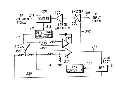
Referring to FIG. 2, there is illustrated a block diagram
of power ~mplifier 203 and its associated controllers, which
are located in the transmitter 107. RF input signal 209
contains information including voice and data sign~lR.
5 Exciter amplifier 205 is an adjustable power amplifier which
amplifies RF input signal 209 in response to amplification
control signal 207 to produce an output which is coupled to
power amplifier 203 and amplified by a fixed gain to produce
RF signal output 214 at a desired output power level. Coupler
10 201 is a conventional electrom~gnetic coupler which couples
power amplifier 203 to ~ntenn~ 105 without c~ ing excessive
loss and which also provides an RF feedback signal 212 which
has an amplitude proportional to the output power level of RF
signal output 214.
1 5 Detecting circuil~y 211 is coupled to RF feedback signal
212 for producing a power level signal 229, which has a
magnitude proportional to the output power level of RF output
signal 214. Detecting circuitry 211 also produces a reference
signal 213 having a magnitude which is substantially equal to
2 0 the DC offset voltage of power level signal 229 when power
amplifier 203 is turned off and not transmitting.
Comparator 215 is coupled to power level signal 229 and
reference signal 213 for producing an output signal 227,
which has a low voltage when the magnitude of power level
2 5 signal 229 exceeds the magnitude of reference signal 213.
Output signal 225 is generated by the DSP 111 and used to pull
up output signal 227. Output signal 225 is high at the
beginning of an active time slot during which radiotelephone
103 or transceiver 101 is transmitting, and is lowered after the
3 0 desired output waveform of RF output signal 214 has been
produced. This causes output signal 227 to be high during an
active time slot prior to power amplifier 203 and exciter
~mplifi~r 205 becoming active. Upon activation of the power
amplifier 203 and the exciter amplifier 205, output signal 227
3 5 becomes low.
O g 5
-7 -
After a predetermined time interval (10 microseconds
in the preferred embodiment) from the beginning of an active
time slot, DSP 111 generates a desired wa~/efo~ and applies
it to digital-to-analog converter 221. D/A converter 221
converts the digital input from DSP 111 into an analog output
signal 231, ~efelled to as an AOC signal. AOC signal 231 and
VGAIN signal 236 are coupled to integrator 219, and
compared and integrated by integrator to produce
amplification control signal 207, which in turn is coupled to
l 0 exciter amplifier 205 for varying its ~mplification level. AOC
signal 231 has a value for producing one of a plurality of
output power levels of the RF output signal 214 from power
amplifier 203. In the preferred embo-liment the l~lefeI-led
waveform is a raised cosine which ramps RF oul~ul signal
l 5 214 of power amplifier 203 smoothly up to its desired output
power level. The AOC signal 231 and the raised cosine
response of the RF output signal 214 are illustrated and
described in more detail in US patent no. 6,150,075.
A saturation control loop, consisting of coupler 201,
2 0 detecting circuitry 211, comparator 217 and DSP 111, prevents
the exciter amplifier 205 and power amplifier 203 from
exceeding their rated output power limits. Comparator 217 is
a saturation detector which compares power level signal 229
to AOC signal 231 to determine if power level signal signal 229
2 5 responds to changes in AOC signal 231. When saturation is
reached, the voltage of power level signal 229 will not change
in response to a change in the voltage of AOC signal 231.
Therefore, when the voltage of power level signal 229 drops
below the voltage of AOC signal 231, output signal 233 of
3 0 comparator 217 is low indicating saturation of exciter
~mplifier 205 and power amplifier 203 . The saturation
comparator output signal 233 is coupled to DSP 111 which
contains a saturation detection algorithm.
According to the saturation detection algorithm, DSP
3 5 111 reduces the voltage of AOC signal 231 in successive steps
~J 120095
.
-8-
until the voltage of AOC signal 231 drops below voltage of
power level signal 229. The operation of the saturation control
loop is described in further detail in U.S. patent 5,278,994,
entitled ~Power Amplifier Saturation Detection and
Correction Method and Apparatus", issued January 11, 1994,
and ~signed to Motorola, Inc.
Referring to FIG. 3, there is illustrated a block diagram
of TC controlled RF signal detecting circuitry 211 embodying
the present invention. Positive coefficient current source 303,
1 0 negative coefficient current source 305, and current mirror
301 in detecting circuitry 211 produce substantially identical
currents Iml and its mirror Im2. Positive coefficient current
source 303 produces current I+ having a positive coefficient of
change with temperature. In the preferred embodiment,
l 5 current I+ has a temperature coefficient of +333 ppm/~C.
Negative coefficient current source 305 produces current I-
having a negative coefficient of change with temperature. In
the ~efe~led embodiment, current I- has a temperature
coefficient of-6000 ppm/~C. Currents I+ and I- and their
2 0 respective temperature coefficients are scaled and summed
in predetermined proportion in current mirror 301 to produce
compensated current Iml. In the l~lefe~led embodiment,
current Iml has a temperature coefficient of-3000 ppm/~C.
Current mirror 301 produces current Im2 as the
2 5 substantially identical mirror of compensated current Iml.
Compensated current Im2 is coupled to anti-clamping
current mirror 309 which applies mirrored currents Ial and
Ia2 of current Im2 to diode detector 311. Diode detector 311
includes two legs, each including a Schottky diode coupled in
3 0 series to a resistor network to signal ground, and each
coupled to one of compensated currents Ial and Ia2. The
Schottky diode in each leg of diode detector 311 is coupled to,
and biased on by the corresponding one of compensated
currents Ial and Ia2. Each leg of diode detector 311 has
3 5 positive coefficient of change with temperature, which is
-9 -
subst~nti~lly offset by the negative coefflcient of change with
temperature of compensated currents Ial and Ia2. In the
preferred embodiment, each leg of diode detector 311 has a
temperature co~fficie~t of +3000 ppm/~C, and compensated
5 currents Ial and Ia2 each have temperature coefflcient of
-3000 ppm/~C. The TC of +3000 ppm/~C is due to the implant
resistors (e.g. resistors 453, 454, 455 and 456) in each leg of
diode detector 311.
The Schottky diode in one leg of diode detector 311 is
1 0 coupled to and half-wave rectifies RF feedback signal 212 to
produce temperature and voltage compensated power level
signal 229, which has a DC level proportional to the oul~ul
power level of RF output signal 214. By utili7:in~ the present
invention, power level signal 229 has a DC level which is
1 5 stable to within 5 mV over tempe~dlu~ r~n~ing from -55~C to
+125~C and over power supply voltage r~ngin~ from 2.7V to
4.75V.
Referring to FIG. 4, there is illustrated a schematic
diagram of the TC controlled RF signal detecting circuitry in
2 0 FIG. 3. Power supply voltage Vcc can range between 2.7V to
4.75V. The ENABLE SIGNAL may be used to turn on or off
detecting circuitry 211 by coupling it to a high or low voltage,
respectively. Positive coefficient current source 303 has been
implemented by NPN transistors 416, 417, 420 and 421.
2 5 Negative coefficient current source 305 has been implemented
by NPN transistor 418. Current mirror 301 has been
implemented by PNP transistors 401 and 403. Currents I+
and I- and their respective temperature coefficients are
scaled to the proper proportion by selection of the values of the
3 0 emitter resistors 472 and 471 of transistors 418 and 421,
respectively.
Anti-clamping current mirror 309 has been
implemented by NPN transistors 411 and 413 and Schottky
diodes 406 and 407. PNP transistor 404 applies current Im2 to
3 5 transistor 411 and 403. NPN transistor 419 supplies base
~2~
- 10-
current to transistor 404. Transistor 411 applies current Ial
to Schottky diode 430, and transistor 413 applies current Ia2 to
Schottky diode 431. PNP transistor 402 b~l~nces the effect of
the base current of transistors 401 and 403 in current mirror
301. NPN transistor 412 b~l~nces the effect of the base
current of transistors 411 and 413 in anti-clamping current
mirror 309. Schottky diode 432 protects the base to emitter
junction of transistor 413 against large positive swings of RF
FEEDBACK SIGNAL 212. During the large positive swings of
1 0 RF FEEDBACK SIGNAL 212, Schottky diode 407 prevents
conduction from Schottky diode 432 through the base to
collector junction of transistor 413, and Schottky diode 406
prevents conduction from Schottky diode 432 through the base
to collector junctions of transistors 411 and 412.
1 5 Diode detector 311 includes in one leg a resistor,
Schottky diode 431, a capacitor to signal ground, and three
resistors coupled in series to signal ground, and in the other
leg a resistor, Schottky diode 430, and three resistors coupled
in series to signal ground. In the preferred embodiment,
2 0 Schottky diodes 431 and 432 and the resistors in each leg have
identical electrical characteristics since they are on the same
semiconductive substrate. The resistors in each leg also have
substantially identical values. Schottky diode 431 is coupled
by capacitor 451 to and half-wave rectifies RF FEEDBACK
2 5 SIGNAL 212 to produce temperature and voltage
compensated POWER LEVEL SIGNAL 229. That is, on
positive excursions of the RF FEEDBACK SIGNAL 212,
Schottky diode 431 conducts and charges capacitor 452 to
produce POWER LEVEL SIGNAL 229. On negative
3 0 excursions of the RF FEEDBACK SIGNAL 212, Schottky diode
431 shuts off and does not conduct. The POWER LEVEL
SIGNAL 229 is taken at the junction of resistors 454 and 455,
VGAIN SIGNAL 235 is taken at the junction of resistors 455
and 456, and the REFERENCE SIGNAL 213 is taken at the
3 5 cathode of Schottky diode 430. REFERENCE SIGNAL 213
2~ J~ 9rl
- 11-
provides a compensated voltage to comparator 215 which
corresponds to the the value of the POWER LEVEL SIGNAL
229 for zero RF FEEDBACK SIGNAL 212.
According to a feature of the present invention,
S transistor 413 of current mirror 309 ~ V~ltS Schottky diode
431 from clamping the voltage at the junction of its cathode
with capacitor 451 and resistor 453. When RF FEEDBACK
SIGNAL 212 is small or not present, current Ia2 provided by
transistor 413 to Schottky diode 431 is 50~LA. How~v~r, when
1 0 RF FEEDBACK SIGNAL 212 is large, current Ia2 provided by
transistor 413 to Schottky diode 431 increases (e.g. to several
milli~qmps) so that the voltage at the junction of capacitor 451
and resistor 453 substantially follows the voltage of RF
FEEDBACK SIGNAL 212, thereby avoiding the clamping
1 5 action of Schottky diode 431.
In the preferred embodiment, TC controlled RF signal
detecting circuitry 211 in FIG. 4 is integrated on a
semiconductive substrate using the MOSAIC 1.5 process.
The TC of the output voltages for POWER LEVEL SIGNAL
2 0 229, REFERENCE SIGNAL 213, and VGAIN SIGNAL 235 are
made substantially zero by the bias currents Ial and Ia2
whose TC is substantially equal but opposite to the TC of the
resistors coupled to Schottky diodes 431 and 432. Since the
output voltages have substantially zero TC and Schottky
2 5 diodes 431 and 432 are matched in characteristics, POWER
LEVEL SIGNAL 229 and REFERENCE SIGNAL 213 are both
temperature and voltage level compensated over a wide
temperature and voltage range.
For the MOSAIC 1.5 process, the TC of the implant
3 0 resistors in TC controlled RF signal detecting circ.~ y 211 in
FIG. 4 is approximately +3000 ppm/~C. Current Im2 is set to
a TC of -3000 ppm/~C to allow the output voltages for POWER
LEVEL SIGNAL 229, REFERENCE SIGNAL 213, and
VGAIN SIGNAL 235 to remain constant over temperature.
3 5 Currents Iml and Im2 are produced by the current generator
9 5
- 12-
made up of transistors 416, 417, 418, 420 and 421 and resistors
471 and 472. The equation of the voltage V471 across resistor
471 is:
S V471 = Vt*ln[(A421*A416)/(A420*A417)],
where A stands for the area of the transistor emitters.
Voltage V471 is the ~~0" portion of the TC equation; the TC of a
~~0" is +3333 ppmt~C (due to Vt = kT/q). Voltage V471 across
1 0 resistor 471 sets the amount of current through the resistor
471, and sets the current in transistors 421 and 417 The TC of
this current can be found by:
TC(I~0/R)=TC~0 - TCR-
1 5
Therefore, the TC of the ~0tR is slightly positive, since TCR is
-3000 ppm and TC~0 is +3333 ppmt~C.
The 0tR current generator is made up of transistor 418
and resistor 472. The base of transistor 418 is at 2Vbe, so the
2 0 voltage drop across resistor 472 is one Vbe. The TC of the
current through transistor 418 is then the comhin~tion of the
TC of one Vbe and the TC of resistor 472. Again, the TC of a 2k
implant resistor is +3000 ppmt~C. The 0tR current generator
TC is then:
TC(I0/R) = TC(0) - TC(R) = [(Ego - Vbe)/(T*Vbe) - 3000] =
-6000 ppm,
where (Ego - Vbe)t(T*Vbe) = -3000 ppm.
The total TC of the current into the reference diode
transistor 401 and thus in current source transistor 403 is
then:
3 5 TC(I0/R)*I0/R + TC(I~0/R)*I~0/R =
- 13 - 2 ~
ITOTAL*TC(ITOTAL),
where ITOTAL is the sum of the two current generators. If
the total current into the reference diode is 50~A, and a TC of
-3000 PPn~~C is needed to cancel the +3000 ppm/~C TC of the
implant resistors in diode detector 311, then:
(-6000 ppm * I0/R) + (333 ppm * I~0~) =
50~A*(-3000 ppm),
1 0
which gives approximately,
I0/R = 26~A, and
I~0/R = 24~A.
The value of resistor 471 in the ~0/R current generator and
the value of resistor 472 in the 0/R current generator are then
chosen to give the current values found above.
The improved TC controlled RF signal detecting
2 0 ci~ iLI~ of the present invention is stable to within 5 mV over
temperature r~n~ing from -55~C to +125~C and power supply
voltage r~nging from 2.7V to 4.75V and can be
advantageously utilized in any radio equipment where it is
necessary to accurately sample the magnitude of an RF
2 5 signal.