Note: Descriptions are shown in the official language in which they were submitted.
2120323
:~ `
The present invention relates to a photoconductor for
electrophotography that has an intermediate layer between
an electrically conductive substrate and a photosensitive
layer to stably obtain excellent electric properties and
excellent image qualities under the condition of repeating
the image-forming process.
From the time that the Carlson Process was invented ~ :
by C. F. Carlson in 1938, technologies associated with
electrophotography have been rapidly progressed and used
in the data-processing systems such as photocopying ~:
machines, laser printers, light-emitting diode printers,
facsimile, and so on.
The Carlson process is known as the
electrophotographic process for image formation, that :~
comprises the steps of~
(i) providing charges uniformly on a surface of the
photosensitive member by means of corona discharge in the
absence of light;
(ii) exposing a charged surface of the photosensitive :
member to light to form a latent image that is a charge
pattern on the photosensitive member that mirrors the
information such as characters and figures to be ~:
transformed into the real imagei
(iii) developing the latent image by applying toner :~
particles that are brought into the vicinity of the latent
image to obtain a toner image; and
`
~ 2120323
(iv) transferring and fixing the developed toner
image on a support medium such as a sheet of paper and
plastics, following that the photosensitive layer is
discharged and cleaned of any excess toner particles using
coronas, lamps, and brushes and scraper blades, or both.
Consequently, the image formation can be repeated by using
the same photosensitive member.
The photosensitive member described above is
generally called as an electrophotographic photoconductor
and is responsible for the photosensitive function such as
increase in electrical conductivity during the light
exposure in the field of the electrophotography. The
photoconductor is generally formed by laminating
photoconductive insulating layer approximately 5-200 ~m in
thickness on an electrically conductive substrate to form
a photoconductor. In this case, the electrically
conductive substrate acts as an electrode in the
photoconductor. In the case of using the step of toner-
image transfer in the process of image formation, it is
20 important that the electric properties of the ~; ;
photosensitive layer should be kept at a constant all the
times in spite of after repeating the steps of discharge,
exposure, development, image-transfer, and cleaning.
~ " .
Taking a mechanical strength of the photoconductor in ;
consideration with the above maters, therefore, the
conventional photoconductors have been mainly prepared by
inorganic photoconductive materials such as selenium,
selenium alloys, zinc oxide, and cadmium sulfate. In
- 2 -
. ~
212~323
recent years, however, there have been much more studies
for using organic photoconductive materials by virtue of
their advantageous features for preparing a light-weighted
flexible layer cost effectively without causing any toxic
effects.
Furthermore, the photosensitive layer of the
photoconductor has been classified into two types in
general. That is, one is formed as a single layer
(hereinafter, referred as a mono-type photosensitive
layer) and the other is formed as a laminate of layers
which are functionally distinguishable (hereinafter ~ ~ Y
referred as a laminate-type photosensitive layer). The
laminate-type photosensitive layer comprises a lower layer
for the function of generating charge carriers and an
upper layer for the function of transporting the charge
carriers. These layers are easily prepared and modified
by selectively using appropriate raw materials to improve
their physical properties such as photosensitivity against
speclfic wavelength of illuminated light and sensitivities
against the spectrum according to the range of wavelengths
~ ~ .
of the illuminated light.
Accordingly, the laminate-type photosensitive layers
have been much more studied that the mono-type one and
used in many kinds of the electrophotographic devices such
as photocopying machines, facsimile machines, and
printers.
More recently, there have been much demands for
miniaturizing the electrophotographic devices and also for
- 3 -
2120323
increasing their printing speeds. For replying to these
demands, the miniaturized devices should be manufactured
so as to keep their abilities of providing good image
qualities by forming the image at the same speed or at the
higher speed compared with that of those currently in use.
In this case, therefore, it is also necessary to
miniaturize a drum of the miniaturized device on which the ~-~
photoconductor will be mounted.
For performing the printing and coping at least at
10 the same speed as that of those currently in use, the -~
small-sized drum must rotate at a higher rate compared
with the conventional one. -~
In the miniaturized device, accordingly, the
photoconductor provided on the small-sized drum can be
used more frequently than that of the conventional one, so ~ -~
that the photoconductor to be installed in the ~ -
miniaturized device should be improved so as to have a
high durability against repetitive usage and a good
respond sensitivity to the illuminated light.
Several photoconductors have been proposed in order
to reply these demands. Most of them include more than
one layer in their photosensitive layer portions. That
is, the photosensitive layer has functionally
distinguishable layers: one contributes to generate an
electric charge by absorbing illuminated light; and the
other contributes to transport the electric charge. The
charge generation layer mainly includes a charge- -~
generating material, while the charge transport layer ~ ~
: .
2120323
mainly includes a charge-transporting material. Besides
the charge-transporting material, the charge transport
layer optionally includes a binder or a stabilizer, or
both. The binder is responsible for forming a membrane
structure while the stabilizer is responsible for
stabilizing the membrane structure by arresting the
progress of oxidation to be caused by ultraviolet light,
ozone, or the like.
Japanese Patent Application Publication No. 55-42380
discloses a photoconductor that has functionally
distinguishable layers, a charge generation layer and a
charge transport layer, and in this case the farmer
includes Chlorodiane Blue as a charge-generating material
and the latter includes a Hydrazone compound as a charge-
transporting material. Both the response rate of the
photoconductor and its durability to last tens of
thousands of cycles of the image formation are mainly
depended on the nature of the charge transport layer.
Accordingly, several materials have been proposed as a raw
~ 20 material for preparing the charge transport material, for
; example Pyrazorine derivatives (the Journal of
Photographic Science and Engineering vol. 21, No. 2, page
73, 1977); Enamine derivatives (the Journal of Imaging
Science vol. 29., No. 1, page 7, 1985 and Japanese Patent
Application Laying-Open No. 63-170651); and Benzidine
derivatives (Japanese Patent Application Laying-Open No.
3-43744 and Japanese Patent Application Laying-Open No.
59-9049). In spite of these investigations, however,
- 5 ~
212~23
these charge-generating materials do not satisfy the
request of providing the photoconductors with both an
excellent durability to the repetitive usage and a good
response speed to the illuminated light.
Consequently, a photoconductor practically used at
the present tlme is generally in the type of organic
photoconductor that has functionally distinguishable
layers: a charge generation layer and a charge transport
layer which are laminated on an electrically conductive
10 substrate in that order. The photoconductor is prepared ~ ~
by the process including the steps of: performing ~ ;
sublimation or vapor deposition of the organic charge- -
generating material on the electrically conductive ~ -~
substrate, or applying and drying a coating solution
prepared by dispersing and dissolving with a binder in an
organic solvent on the electrically conductive substrate
to form the charge generation layer; and applying and
drying another coating solution prepared by dispersing and
dlssolving a charge-transporting material with a binder in
an organic solvent on the charge generation layer to form
the charge transport layer. The photoconductor that has `
the Iaminate structure thus obtained is enough to perform
the process of image formation. In the practical use,
however, it is important to form images without any
defects and also it is important to keep good image
qualities during the period of repeating the usage.
Therefore the photoconductor should be formed as a uniform
structure without any defects to obtain stable electric
- 6 -
' ':' '' ~ .~
2120323
properties thereof and sufficient durability to last of
tens of thousands of cycles of the image formation.
By the way, the function of the charge generation
layer is to absorb the illuminated light and generate ~ -;
electron carriers. These electron carriers move quickly
to both the electrically conductive substrate and the
charge transport layer. It is required that the charge
generation layer does not trap free carriers during their
movements for injecting them into the electrically
conductive substrate and the charge transport layer.
Therefore, it is preferable that the charge generation
layer is formed as thin as possible. The charge
generation layer used in the conventional photoconductor
is generally formed as a thin film with a thickness of in
the order of sub microns, so that the charge generation
layer is easily affected by troubles on a surface of the
electrically conductive substrate, such as unstable
electric properties, an irregular shape, impurities, and -
roughness thereof. However it is difficult to make the
substrate without causing the troubles described above.
Consequently these troubles affect the photosensitive
layer to deteriorate the image qualities by causing
whiteness of non-imaged areas and blackness and non
uniform appearance of the imaged areas in the copy.
In general, the electrically conductive substrate is
formed as a drawn cylindrical tube of aluminum alloy, or a
cylindrical tube having a surface smoothed by means of
- 7 -
2120323
cutting, grinding and polishing, but it is difficult to
avoid the troubles described above. ;~
Up to the present time, the conventional
photoconductor has been modified by providing an
intermediate layer between the photosensitive layer and
the electrically conductive substrate for obtaining a
smooth and uniform surface of the charge generation layer
and also for suppressing the deterioration of charge~
holding properties of the photoconductor. The
deterioration can be caused by injecting holes (which are
required for converting light to electron-hole pairs) from
the electrically conductive substrate to the
photosensitive layer. In this case, the intermediate ~-~
layer is typically made of an N-type resin having a low
electric resistance, such s solvent-soluble polyamide,
polyvinyl alcohol, polyvinyl butyral, and casein. Only ~
for suppressing the deterioration of charge-holding ~ ~;
properties of the photoconductor, the intermediate layer ~
can be formed as thin as possible by using one of the N- ~;
type resins for the intermediate layer. For example, the
effective intermediate layer can be formed so as to have a
thickness of 0.1 ~m or under, but thick enough to make a
uniform surface of the charge generation layer for
covering the rough or contaminated surface of the
electrically conductive substrate without causing non
uniform distribution of the coating solution of the charge
generation layer. Conse~uently, the intermediate layer ~ ~
- 8 - - ~ ;
-' 212û323 -~
should be formed so as to have a thickness of at least 0.5
~m, or preferably 1 ~m or over if required.
However, the thin resin layer formed by using one of
the resins described above rises the residual potential
and changes the electric properties of the photoconductor
under the environmental condition of at a low temperature
and a low humidity or at a high temperature and as high
humidity.
These troubles are due to the changes of electric
resistance of the resin layer because these changes are
depended on the moisture content of the resin layer that
has an affinity for moisture (i.e., hygroscopic
properties) and the absorbed water molecules in the resin
dissociate into hydrogen ions and hydroxyl ions. These
ions are responsible for the ionic conductance which
occupies the greater part of the electroconductance.
It has been proposed that a polyamide resin is one of
the suitable raw materials for preparing the intermediate
layer. In spite of its thickness, for that reason, it has
a low electric resistance thereof. The resistance is only
slightly changed when its environmental condition is
changed. In the case of solvent-soluble polyamide resins
which can be used as suitable raw materials, for example,
their structures are specified in the documents of
Japanese Patent Application Laying-Open No. 2-193152;
Japanese Patent Application Laying-Open No. 3-288157;
Japanese Patent Application Laying-Open No. 4-31870; and
others. In addition, several other documents such as
_ g _
-"` 212~323
Japanese Patent Application Publication No. 2-59458,
Japanese Patent Laying-Open No. 3-150572, and Japanese
Patent Application Laying-Open No. 2-53070 disclose that
the changes of electric resistance due to the
environmental changes are limited by adding an appropriate ~;
additive to the polyamide resin. Furthermore, Japanese
Patent Application Laying-Open No. 3-145652, Japanese
Patent Application Laying-Open No. 3-81778, Japanese
Patent Application Laying-Open No. 2-281262, and other ~`
documents disclose mixtures of polyamide resin and another
kind of resin for adjusting the electric resistance to
protect the layer form the effects of the changes of the
environmental conditions. However, the intermediate layer
comprises the polyamide resin as one of the main
components so that the electric properties of the layer
can be influenced by a degree of temperature and humidity
in the surroundings.
In addition to the polyamide resin, several materials
have been proposed as a raw material of the intermediate
layer, such as cellulose derivatives (Japanese Patent
Application Laying-Open No. 2-238459); polyether urethane
(Japanese Patent Application Laying-Open No. 2-115858,
Japanese Patent Application Laying-Open No. 2-280170);
polyvinyl pyrolidone (Japanese Patent Application Laying-
Open No. 2-105349) and polyglycol ether ~Japanese Patent
Application Laying-Open No. 2-79859).
For keeping a moisture content in the resin layer at
a constant against the surroundings, a cross-linking resin
- 10 - ,.. , ~. ~;
~ 212~323
~ .
has been also proposed as a raw material of the
intermediate layer, such as melamine resin (Japanese
Patent Application Laying-Open No. 9-22966, Japanese
Patent Application Publication No. 4-31576, and Japanese
Patent Application Publication No. 4-31577) and phenol
resin (Japanese Patent Application Laying-Open 3-48256).
The intermediate layer formed by using one of the
materials described above is useful when it is formed as
an extremely thin film. However, the resistance of the
photoconductor, which is the cause of increasing the
residual potential, can be increased when it is formed as
comparatively a thick film with a thickness of in the
order of several ~m.
One of the ways for eliminating the problems
described above to form the intermediate layer is to use a
material having an electric conductivity in the type of
electronic conduction instead of ionic one. For this
purpose, Japanese Patent Application Publications No. 1-
51185, 2-48175, 2-60177 and 2-62861 propose the processes
in which the intermediate layers are formed by dispersing
the electrically conductive powders such as tin oxide and
indium oxide in the resin. In spite of these proposals,
however, it is difficult to make a uniform dispersion of
the electrically conductive particles in the resin
solution to be applied on the conductive layer.
Furthermore, the resin solution comprising the particles
cannot store well because they are easily segregated and
settle to the bottom in the solution, so that the
2120323
particles tend to protrude as mlnute projections from a
surface of the applied solution during the step of forming
the intermediate layer on the conductive substrate. In
this case, the intermediate layer with a rough surface can
be obtained and the image qualities of the photoconductor
can be deteriorated. For improving the image qualities,
organic metal compounds are used instead of the above
electrically conductive particles. For example, Japanese
Patent Application Publication No. 3-4904 and Japanese
Patent Application Laying-Open No. 2-59767 disclose the
steps of forming the intermediate layer by applying the
solution prepared by dissolving the organic metallic -
compounds and the resin in the organic solvent,
nevertheless the solution is not stable enough to provide
a uniform surface of the layer. Consequently there are
many problems to be solved for producing the
photoconductors on a large scale.
An object of the present invention is to provide a
photoconductor for electrophotography that has excellent
electric properties and image qualities without causing
any troubles by the environmental conditioni and an
increased productivity on a large scale.
There is provided an electrophotographic
photoconductor comprising~
an electrically conductive substrate;
a photosensitive layer formed on the electrically
conductive substrate; and
- 12
-~ 212~323
an intermediate layer formed between the electrically
conductive substrate and the photosensitive layer, wherein
the intermediate layer is made of a hardened film
comprising an amino resin.
Here, the hardened film may be formed by hardening
the amino resin with a catalyst comprising at least one
acid selected from a group of organic and inorganic acids
and latent acids thereof.
The organic acid may be selected from a group of
aromaticsulfonic acid, alicyclicsulfonic acid, and
mixtures thereof.
The amino resin may be a compound selected from a
butylated urea resin, a butylated melamine resin, a
butylated benzoquanamine resin, and a butylated
benzoguanamine resin, and a butylated benzoguanamine co-
polymer resin, which is prepared by reacting alcohol with
a methylol compound obtained by a reaction between
formaldehyde and a compound selected from a group of urea ;
compounds including dicyandiamide, urea, and thiourea and
triazine compounds including melamine, isomelamine,
benzoguanamine, and acetoguanamine.
The aromaticsulfonic acid and the alicyclicsulfonic
acid may be compounds in which sulfonic groups are
directly bound to aromatic and alicyclic group,
respectively, and selected from a group of benzenesulfonic
acid, paratoluenesulfonic acid, 2-naphthalenesulfonic
acid, dodecylbenzenesulfonic acid,
dinonylnaphthalenesulfonic acid,
- 13 -
--` 2120323
dinonylnaphthalenedisulfonic acid, camphasulfonic acid,
anthraquinone-1,5-disulfonic acid,
anthraquinone-2,6-disulfonic acid, anthraquinone-2-
sulfonic acid, and derivatives thereof in which aromatic
and alicyclic groups are bound to one of aryl, alkyl, and
aralkyl groups.
The intermediate layer may comprise:
5-100 parts by weight of the organic acid selected
from a group of aromaticsulfonic acid, alicyclicsulfonic
acid, and a mixture thereof with respect to 100 parts by
weight of the amino resin.
The inorganic acid may be selected from a group of
hydrochloric acid, hydrofluoric acid, hydrobromic acid,
sulfuric acid, phosphoric acid, and boric acid; and the
inorganic acid is comprised in the catalyst with or -~
without the organic salt.
The organic acid may be comprised in the catalyst
with a second organic acid selected from a group of acetic
acid, oxalic acid, succinic acid, adipic acid, benzoic
acid, 2-naphthalincarbocylic acid, orthofutalic acid,
isofutalic acid, trimellitic acid, pyromellitic acid,
maleic acid, fumaric acid, itaconic acid, linolic acid,
endomethylene tetrahydrophtalic acid, and latent acids
thereof, with or without the inorganic acid.
The catalyst may comprise:
0.1 - 10 mol of an acid selected from the second
organic acid, the inorganic acid, and a mixture thereof -~
with respect to 1 mol of the organic acid selected from a
: .
- 14 -
2120323
group of aromatic sulfonic acid, alicyclic sulfonic acid, ~-
- and mixtures thereof.
The intermediate layer may further include a compound
selected from a group of iodine, ferric chrolide, and a
mixture thereof.
The intermediate layer may further include a compound
selected from a group of alkyd resin and phenol resin.
The intermediate layer may further include a filler
selected from a group of titanium oxide, aluminum oxide,
kaolin, talc, and silicon oxide.
The photosensitive layer may be in the type of having
functionally distinguishable layers and may be composed of
a charge generation layer and a charge transport layer.
The charge generation layer may include at least one
charge-generating material selected from a group of: -
inorganic charge-generating materials including selenium-
tellurium and selenium-arsenic; organic charge-generating
materials including azo pigment, disazo pigment, perynon
pigment, perylene pigment, anthanthrone pigment,
phtalocyanine pigment, pyrylium pigment, and squaraines
pigment.
The charge transport layer may be composed of:
a compound selected from a group of indole
derivatives, enamine compounds, amine compounds, hydrazone
- compounds, styryl compounds, butadiene compounds,
triphenylmethane compounds, and pirazoline compounds; and ~ ;
a binder resin which is mutually soluble to the
compound, preferably selected from a group of ;~
- 15 -
~ 2120323
polycarbonate resin, polystyrene resin, styrene resin, and
acrylate resin.
The electrically conductive substrate may be made of
a material selected from: non-conductive materials having
a surface treated to be electrically conductive by a
treatment selected from a metal deposition, a metal
plating, and an application of an electrically conductive
paint, including plastic, paper, carbon powder dispersed
plastics and glass; and conductive materials including
iron, nickel, and aluminum.
The above and other objects, effects, features and
advantages of the present invention will become ore
. . .
apparent from the following description of embodiments
thereof taken in conjunction with the accompanying ;
drawings.
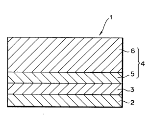
Fig. 1 shows a cross sectional plan view of a
photoconductor for electrophotography in accordance with
the present invention.
As shown in Fig. 1, a photoconductor 1 as one of the
-
preferred embodiment of the present invention is in the
type that a photosensitive layer 4 is consisted of
different layers (i.e., a charge generation layer 5 and a -~
charge transport layer 6) which are functionally
distinguishable. Therefore the photoconductor 1 has a
laminate structure in which an intermediate layer 3, the
charge generation layer 5, and the charge transport layer
- 16 -
~ 212~323
6 are laminated on an electrically conductive substrate 2
in that order. It is noted that the present invention is
not limited in the laminate type as described above but
also it is possible to provide a photoconductor in the
type of mono-layer in which a photosensitive layer is not
divided into two portions.
The electrically conductive substrate 2 serves as an
electrode of the photoconductor 1 and as a support for
other layers 3, 5, and 6 formed thereon. Also, the ~-
electrically conductive substrate 2 may be in the form of
a cylinder, a plate, or a film, and also may be made of a
metallic material such as aluminum, stainless steel,
nickel, or the like; or other material such as plastics,
glass, paper, or the like that has a surface treated to be i
electrically conductive by means of metallization, metal
plating, electrically conductive coating, or the like for
example carbon powder dispersed plastics.
The charge generation layer 5 includes a charge~
generating material select from: inorganic charge~
generating materials such as selenium-tellurium, and
selenium-arsenic; and organic charge-generating materials
such as azo pigment, squaraines pigment, pyrylium pigment,
perylene pigment, anthanthrone pigment, phtalocyanine
pigment, and titanylphthalocyanine pigment, but not
limited to those materials.
A predetermined amount of the charge-generating
material is provided into a layer on the electrically
conductive substrate by means of vacuum evaporation or
- 17 -
212~2~
applying and drying a dispersion of the charge-generating
material in a solvent with or without a resin binder on
the substrate.
The resin binder to be included in the charge
generation layer is selected from any materials which can
be easily formed as electrical-insulating films and fit to
the layer formation, for example polyvinyl resin (such as
polyvinyl formal, polyvinyl acetal and polyvinyl butyral);
acrylic resin; polyester resin; polycarbonate resin; vinyl
10 chloride copolymerized resin; vinyl-acetate copolymerized ~ :
resin; and silicone resin. It is preferable to use lO to
300 weight % of the resin binder per a total volume of the
charge generation layer. In addition to the resin binder,
an additional agent can be further included in the charge
generation layer if required, for example a plasticizer
(such as paraffin halide) and a pin-hole preventive agent
(such as dimethyl phthalate).
The charge generation layer is prepared as follows.
The charge-generating material selected from the
20 inorganic or organic materials described above is applied ~`
on the electrically conductive substrate by means of -~
vacuum deposition to form a layer 0.01-1 ~m in thickness.
Alternatively, it is prepared by applying the solution
including the resin binder or the additional agent
described above, or both by means of using sand mill,
atritor, paint shaker or the like with the method of spray
coating, dip coating or the like to form a layer 0.01-3 ~m
in dry thickness.
- 18 -
212D323
The charge transport layer 6 is made of a charge
transport material selected from a group of amine
compounds, hydrazone compounds, styryl compounds,
butadiene compounds, enamine compounds, diamine compounds,
benzidine compounds, tryphenylmethane compounds, ;~
pyrazoline compounds, and indole derivatives disclosed in
the U. S. Patent Application Serial No. 08/05,988. Also,
the charge transport layer is prepared by the steps of:
dissolving the charge-transporting material with a resin
binder in a solvent to make a coating solution; applying
the coating solution on the electrically conductive
substrate; and drying the coating solution to form a layer
5-40 ~m in thickness. The resin binder usable in the
charge transport layer can be selected from a group of
polycarbonate resin, polyester resin, acrylic resin,
styrene resin, and the like but not limited to these
resins.
The intermediate layer 3 is made of a hardened
; membrane prepared by hardening an amino resin as a main
component with a catalyst containing aromatic sulfonic
acid and/or alicyclic sulfonic acid. According to this
specified formula, the intermediate layer provides a
photoconductor with excellent electric properties compared
with the conventional one prepared by hardening the amino
resin with the other kind of acids. That is, the
intermediate layer 3 of the present invention is stable
under the environmental changes and its residual potential
takes comparatively a low value whatever the layer has a
-- 19 -- ..
~ 2120323
large thickness, for example 10-20 ~m. According to the
present invention, in addition, troubles such as
increasing of the residual potential and decreasing of
charging properties of the intermediate layer cannot be
observed after repeating the cycles of image formation.
Furthermore, the photoconductor of the present invention
shows excellent electric properties of providing good
image qualities without causing any troubles by the
surroundings (for example at high temperature and humidity ;
or low temperature and humidity) during the period of
repeating the cycles of image formation.
The amino resin mentioned above is prepared as
follows. That is, a urea compound selected from dicyanic
diamide, urea, thiourea, and the like or a triazine
compound selected from melamine, isomelamine,
benzoguanamine, acetoguanamine and the like is reacted
with formaldehyde to obtain a methyrol compound. The
methyrol compound is further treated with butanol,
isobutanol, or the like to obtain a butyl etherated
compound which can be used alone or as a mixture or a co-
condensed compound.
The aromaticsulfonic acid or alicyclicsulfonic acid
is a compound in which sulfonic group is directly bound to
aromatic or alicyclic group, for example benzenesulfonic
acid, para-toruensulfonic acid, 2-naphthalenesulfonic
acid, dodecylbenzene sulfonic acid,
dinonylnaphthalenesulfonic acid,
dinonylnaphthalenedisulfonic acid, camphasulfonic acid,
- 20 -
-`~ 2120323
anthraquinone-1,5-disulfonic acid, anthraquinone-2,6-
disulfonic acid, and anthraquinone-2-sulfonic acid. In
addition, derivatives that have aromatic or alicyclic
group with aryl, alkyl, or aralkyl group can be also used.
These compounds of sulfonic acid act as a catalyst
for hardening the amino resin and also they improve an ~ ~
electrical conductivity of the amino resin. ~ -
The amount of the sulfonic acid enough to harden the
amino resin is depended on types of the amino resin and
the sulfonic acid to be used, but in general 5-10 weight %
of the sulfonic acid with respect to 100 weight ~ of the
amino resin is preferably used. In the case of preparing
the intermediate layer by using under 5 weight % of the
sulfonic acid, the amino resin cannot be hardened
sufficiently because the coating solution to be formed as
a charge generation layer is absorbed into the
intermediate layer. Consequently, the intermediate layer
thus obtained does not show a low electrical conductivity.
In the case of preparing the intermediate layer by using
over 5 weight % of the sulfonic acid, on the other hand,
the intermediate layer cannot be formed as a smooth and
uniform membrane because it becomes too hard.
In this invention, the specified compounds of
sulfonic acid described above are used as a catalyst for
hardening the amino resin. However, these compounds can
` be also used as one in the form of a latent acid such as
~; amine salt and ammonium salt.
- 21 -
- : .
,~
~-~ 2120323
Furthermore, it is possible to mix the sulfonic acid
compound described above with an additional compound that
has been known as a catalyst for hardening the amino
resin. Such additional compound can be selected from
inorganic acids, organic acids, and latent acids thereof
such as amine salt and ammonium salt. Accordingly, a
hardness of the intermediate layer is arbitrarily assigned
by shifting the hardening rate or the cross-linking rate
of the amino resin by selecting the type and the amount of ;
acid to be added. The inorganic acid can be selected from
a group of hydrochloric acid, hydrofluoric acid,
hydrobromic acid, sulfuric acid, phosphoric acid, boric
acid, and latent acids thereof. Also the organic acid can
be selected from acetic acid, oxalic acid, succinic acid, -~
adipic acid, benzoic acid, 2-naphthalenecarboxylic acid, -
orthophthalic acid, isophthalic acid, trimellitic acid,
pyromellitic acid, maleic acid, fumaric acid, itaconic ;
acid, linolic acid, endomethylene tetrahydrophtalic acid,
acid anhydrides thereof, and latent acids thereof such as
amine salt and ammonium salt. These inorganic and organic
acids can be used individually or as a mixture thereof.
; It is preferable that the catalyst comprises 0.1-10 mol of ~-
the additional compounds with respect to 1 mol of the
sulfonic acid. When the amount of the additional
compounds is under 0.1 mol, the hardness of the coated
layer is lowered. When the amount of the additional
compounds is over 10 mol, the sulfonic acid does not
- 22 -
212~323
effect on the layer well and increases the residual
' potential of the photoconductor.
These specified sulfonic acids not only act as a
catalyst for hardening the amino resin but also act as one
for lowering a resistance of the applied solution.
Furthermore, the resistance can be further decreased by
adding an agent such as iodine or ferric chloride.
Therefore the amount of the sulfonic acid can be
comparatively lowered by adding such agent and thus
physical properties of the membrane obtained by hardening
the amino resin such as adhesive properties, hardness,
strength, and resistance to solvents can be improved.
Furthermore, the intermediate layer may further
include alkyd resin, phenol resin, or the like to improve
~ f;
a strength of adhesion between the substrate and the
intermediate layer, between the charge generation layer
and the intermediate layer, or between the intermediate
layer and a blocking layer if required. The blocking
layer is a thin film mainly comprising polyamide resin
which is soluble in alcohol. The blocking layer is
provided between the intermediate layer and the charge
` ~ generation layer. The phenol resin mentioned above may be
~; included as a resol type which is prepared by condensing
phenol with excess formaldehyde.
The intermediate layer may further comprise a filler
for avoiding a generation of drips of the applied solution
on the substrate, and also for avoiding a generation of
moire on the image as a result of reflecting the light
- 23 ~
212~323
from the substrate when the intermediate layer is prepared
for the photoconductor used in the electrophotography
using coherent light for the exposure. In this case, the
filler can be selected from several compounds such as
titanium oxide, aluminum oxide, kaolin, talc, and silicon n~
oxide. ~
According to the present invention, the intermediate ~ -
layer is formed as follows. A mixture of indispensable
main components (i.e., amino resin, aromaticsulfonic acid
10 and/or alicyclicsulfonic acid) and various materials `
described above is dissolved and dispersed in an
appropriate solvent such as a mixture of butanol and
xylol; tetrahydrofuran; and methanol to prepare a coating
solution. The coating solution is applied on the
electrically conductive substrate by means of splay
coating, dip coating or the like, and then the coating
solution is heated so as to make a sufficient hardening of
the solution to be formed as a membrane. In general. the
heating is performed at a temperature of 80-150 C,
preferably 120-130 C, for 20-60 minutes.
The intermediate layer thus obtained has a sufficient
low electric resistance which is hardly ever effected by
changing the surroundings at high temperature and humidity
or at low temperature and humidity. Therefore, the
electric properties of the intermediate layer can be
hardly ever effected at all in all cases whatever it is
formed as a thick layer (e.g., 10-20 ~m in thickness) and
used over and over. That is, for example the electric
- 2~
.:
212~323
properties such as charge potential, photosensitivity, and
residual potential of the photoconductor do not be
effected by the repetitive usage. In addition, many
inhomogeneous, shape-defective, rough, and impure regions
formed on the surface of the photoconductive substrate can
be covered with the intermediate layer so that the
photosensitive layer can be formed so as to reduce
membrane defects and make it uniform throughout. In the
case of the photoconductor of the functionally deviated
layer type, in which the photosensitive layer is formed by -
laminating the charge transport layer on the charge
generation layer, the charge generation layer can be
easily formed as a thin îilm which is uniform throughout. ~-
Consequently the photoconductor for constantly providing
excellent image qualities can be obtained, and also it is
very rare to provide the images having defects.
According to the present invention, as stated above,
a preferable photoconductor has functionally distinguished
layers in which a charge generation layer and a charge
transport layer are laminated on an electrically
conductive substrate in that order. In the
photoconductor, the charge generation layer is formed as a
coated film with a thickness of 0.1-1 ~m by drying a
coating solution on the intermediate layer described
above. The coating solution is prepared by dispersing a
pigment selected from phtalocyanine pigment, anthanthrone
pigment, perynon pigment, perylen pigment, azo pigment,
disazo pigment, and so on in an appropriate binder resin. ~ -~
- 25
212~323
Then the charge transport layer is formed on the charge
generation layer having a thickness of 5-40 ~m by applying
and drying a solution prepared by dissolving a binder
resin such as polycarbonate, polyester, polystyrene, or
styrene acrylate, which is well-suited with a material~`
selected from a group of amine compounds, hydrazone
compounds, enamine compounds, and so on.
The amino resin mentioned above is prepared as
follows. That is, urea, melamine, isomelamine,
benzoquanamine, acetoguanamine or the like is mixed with
an excess formaldehyde. The obtained mixture is treated
with methylol and is subjected to a methylene condensation -
in a large amount of butanol in the presence of alkali
catalyst. The condensed compound is further treated with
butyl ether to obtain the amino resin. In this case, the
degree of the condensation is varied according to the
amount of the excess formaldehyde and a strength of the
alkali catalyst. In general, the condensed compound of
about 2,000-4,000 average molecular weight can be
obtained. When the reaction is performed in the presence
of only acidic catalyst, on the other hand, the condensed
compound of amount 1,000 average molecular weight can be
obtained.
The amino resins to be obtained by the process ;
described above have been well known as butylated urea
:::
resin, butylated melamine resin, butylated benzoquanamine
resin, and co-condensed resin between butylated melamine
and benzoguanamine. These resins are commercially
- 26 - .
2120323
available, for example "Uban" (trademark, manufactured by
Mitsui Toatsu Chemicals Co., Ltd.) and "Super Bekamine"
(trademark, manufactured by Dai Nippon Ink Chemical
Industrials Co., Ltd.).
<Examples 1-11>
Following materials were used for preparing the
intermediate layer.
1 0 ' ~ '
(1) Amino resin
Sample A-l: Melamine resin which was prepared as
follows.
A reaction mixture of melamine (126 g), n-butanol
(~00 g), paraformaldehyde (150 g), and lN-HCl solution
(0.3 g) was dehydrated by reflux for 2 hours at 100 C and
n-butanol was distilled off, resulting that a resin
solution with 50 weight % solidified portion was obtained
and referred as a sample A-1 (according to the analysis, -
the number-average molecular weight 1500, methyrol group
1.7, and butylether group 2.0).
Sample A-2: Uban 20 (trademark) manufactured by
Mitsui Toatsu Chemicals Co., Ltd. ;
Sample A-3: Uban 91-55 (trademark) manufactured by
Mitsui Toatsu Chemicals Co., Ltd.
- 27 - ~
:-: ''~ ' ' .
2120323 ~
~ `
Sample A-4: Supper Beckamine TD-126 (trademark) :.
manufactured by Dai Nippon Ink Chemical Industrials Co., :~
Ltd. - ~
Sample A-5: Beckamine P-138 (trademark) manufactured .
by Dai Nippon Ink Chemical Industrials Co., Ltd.
(2) Aromaticsulfonic acid or alicyclicsulfonic acid
:.,~' ~',,
Sample B-1: dinonylnaphthalenedisulfonic acid
Sample B-2: dinonylnaphthalenedisulfonic acid
ammonium salt
Sample B-3: dodecylbenzenesulfonic acid
Sample B-4: camphasulfonic acid
(3) Acids except sulfonic acid
Sample C-1: phosphoric acid
Sample C-2: ammonium chloride
Sample C-3: trimellitic anhydride
Sample C-4: itaconic acid ~ :
Sample C-5: maleic anhydride
Sample C-6: ammonium phthalate
(4) Agents for lowering the resistance :.
Sample D-l: iodine
Sample D-2: ferric chloride
An intermediate layer was formed on an aluminum
cylinder (30 mm outer diameter, 28 mm inner diameter,
- 28 -
~'~ ' ;.
-` 2120323
260.5 mm length) with a surface roughness of RmaX = 1.0
mm. Then the aluminum cylinder was treated with one of
the coating solution T-1 - T-11 which were prepared from
the samples A-1 - A-5, samples B-1 - B-4, samples C-1 - C-
6, and samples D-1 and D-2, as shown in Table 1 below, by
the method of dip coating. The solution applied on the
cylinder was subjected to a sintering process for
hardening the solution to make the intermediate layer
under one of the conditions in Table 2 below. The
intermediate layers U-1 - U-11 as listed in Table 2. Each
value of the concentration in Table 1 was calculated as a
proportion in relation to the solvent which is a mixture `~
of toluene and butanol (50 : 50).
<Comparative Examples 1-2>
The intermediate layers u-1 and u-2 were prepared by
the same method as that of the examples 1-11, excepting
their composition of the coating solution t-1 and t-2, as
shown in Table 1 below. That is, each intermediate layer
was prepared by the steps of treating a surface of the
aluminum cylinder with one of the coating solutions (t~
or t-2) by the method of dip coating and dried, and
subjecting the surface to a sintering process for
hardening the solution to make an intermediate layer u-1
or u-2, under the condition shown in Table 2 below.
- 29 -
. .,, . ~ . ... ..... . .. .
~ 2120323
Table 1:
SolutionComposition (parts by weight)
No.
Amino Sulfonic Other Agent Conc.
resin acid acid (%)
T-1 A-1(100) B-1(20) 50
T-2 A-1(100) B-2(25) 50
T-3 A-3(100) B-3(30) 50
T-4 A-2(100) B-4(30) C-1(5) 50
T-5 A-2(100) B-2(25) C-2(5) 50
T-6 A-2(100) B-1(10) C-3(10) 50
T-7 A-2(100) B-2(10) C-6(10) 50
T-8 A-2(100) B-3(10) D-1(5) 30
T-9 A-2(100) B-1(5) C-5(10) D-1(5) 30
T-10 A-2(100) B-1(5) C-5(10) D-2(5) 30
T-ll A-2(100) B-1(5) C-4(10) D-l/D-2 40
(5/5)
t-lA-2(100) phthalic 30
acid(20) :`
t-2A-3(100) trimellic :.
acid(20) 50
- 30 -
2120323
Table 2:
Intermediate Hardening Membrane thickness
layer No. condition (~m)
" : ' -
U-l 130 C X 2 hours 10
U-2 ditto 15
10 U-3 ditto 20
U-4 ditto 20
U-5 ditto 15
U-6 100 C x 1 hour 10
U-7 190 C x 1 hour 10
U-8 130 C x 2 hours 15
U-9 ditto 20
U-10 , ditto 10
U-11 ditto 10
u-l ditto 15
20 u-2 ditto 15
' ~ ''' ~'
The photoconductor was prepared as follows.
The aluminum cylinder having the intermediate layer
described above was dipped into a solution prepared by :~
dispersing the following compounds by paint shaker to form
a charge generation layer of 0.2 ~m in dried thickness.
The compounds were 1 parts by weight of X-type non~
metal phthalocyanine which was commercially available as
- 31 -
2120323
.
"Fastogen Blue 8120 B" (trade mark, manufactured by Dai
Nippon Ink Chemical Industrials Co. Ltd.);
1 parts by weight of co-polymerized vinyl chloride
resin commercially available as "MR-110" (trademark,
manufactured by Nippon Zeon Co., Ltd.); and 100 parts by
weight of methylene chloride.
Furthermore, the aluminum cylinder is dipped into a
solution prepared by dissolving 10 parts by weight of
polycarbonate resin commercially available as "Iupiron
PCZ-300" (trademark, manufactured by Mitsubishi Gas
Chemicals Co., Ltd.) and 10 parts by weight of N,N-
diethyl-aminobenzoaldehydediphenylhydrazone in 80 parts by
weight of tetrahydrofuran to obtain a charge transport -
layer of 20 ~m in dry thickness, resulting that each
photoconductor of Examples 1-11 and Comparative examples 1
and 2 was obtained.
The electrophotographic properties of the each
photoconductor was evaluated by using a process-
examination device for photoconductors. The
20 photoconductor was placed in the device as a sample. The ~ ~
sample was negatively charged by corotoron at -600 v and
then it was rotated at a peripheral speed of 78.5
mm/second. Initial potential (Vo) was defined as a level
of potential at an initial period in the absence of light.
The sample was left in dark for 5 seconds, and then a rate
of the potential at an initial period in the absence of
light. The sample was left in dark for 5 seconds, and
....
then a rate of the potential retention (Vks(~)) was
b ~
2120323
calculated by measuring potentials during the period.
Bright potential (Vi) was defined as a level of potential
at 0.2 seconds after starting the irradiation with light
of a wavelength of 780 nm and a luminous flux density of 2
~W/cm2. Furthermore residual potential (Vr) was defined
as a potential measured after the irradiation for 1.5
seconds. The process including the charging and the
development was repeated 10,000 times. Electric
properties of the photoconductor at the initial stage and
at the stage of repeating the process 10,000 times were
listed in Table 3. ~--
Table 3
Initial After 10,000 repetitions
No . Vo ~V) Vk5 (%) Vi (V) Vr (V) VO (V) Vk5 (%) ~7i (V) Vr (V)
Exp.l -650 89 -50 -20 -640 87 -70 -25 `
20 Exp.2 -670 88 -52 -25 -650 92 -80 -36 -
Exp.3 -650 84 -49 -30 -630 89 -71 -34
Exp.4 -660 89 -49 -35 -650 94 -74 -40
Exp.5 -630 87 -40 -10 -610 93 -49 -21
Exp.6 -650 90 -50 -25 -640 89 -60 -30
Exp.7 -640 91 -56 -28 -630 90 -59 -30
Exp.8 -620 92 -51 -10 -600 90 -55 -18
Exp.9 -600 89 -49 -8 -590 88 -56 -20
Exp.10 -610 88 -48 -6 -600 87 -52 -16
Exp.ll -600 89 -46 -9 -580 87 -56 -17
30 Comp.l -670 87 -100 -80 -600 95 -140 -120
Comp.2 -650 89 -120 -100 -600 90 -160 -140
::, -.
- 33 ~
`-` 2120323
From the results listed ln Table 3, the intermediate
layers of Comparative Examples 1 and 2, which do not
comprise the sulfonic acid in their intermediate layer,
show high residual potentials and poor abilities of
maintaining their electric properties during the
repetitive usage.
Furthermore, characteristic changes of the
photoconductor were observed under the circumstances of: : :
high temperature and humidity (H.H: 35 C, 85 % RH); and
lQ low temperature and humidity (L.L: 10 C, 50 % RH). The
results were listed in Table 4. : ::~
. ~:
Table 4: -;~ :
L.L . H.H ;~
No . Vo (V) Vk5 ( 96 ) Vi (V) Vr (V) Vo (V) Vk5 ( % ) Vi (V) Vr (V)
Exp.1 -660 91 -100 -40 -640 90 -S0 -20
Exp.2 -685 92 -90 -45 -645 89 -60 -32
Exp.3 -670 93 -97 -38 -635 88 -50 -30
Exp.4 -680 90 -102 -46 -650 89 -54 -35
: Exp.5 -640 89 -100 -41 -620 88 -57 -28 :
~ : Exp.6 -660 91 -90 -50 -640 89 -46 -20
Exp.7 -650 93 -94 -48 -630 90 -49 -20 ~-
Exp.8 -640 94 -97 -46 -600 90 -24 -10
:i Exp.9 -620 90 -76 -39 -590 87 -37 -12
Exp.10 -630 91 -68 -40 -590 86 -30 -6
. ~ Exp.ll -620 92 -74 -44 -580 89 -32 -7
: 30 Comp.1 -690 92 -180 -160 -590 89 -80 -60
Comp.2 -700 94 -190 -140 -600 85 -100 -80
::' ~" ' ~ '.-
- 34
.
2120323
As shown in Table 4, the values of Vo and Vi vary
extensively when the intermediate layer does not comprise
the sulfonic acid.
The photoconductor thus obtained was placed in the
laser-beam printer "Laser Jet 111" (trademark,
manufactured by Hewlett Packerd Co., Ltd.).
Image qualities are measured by counting number of ~-
black dots of 0.2 mm or over in diameter produced on the
area with four equal sides of 90 mm in a surface of the
photoconductor. The measurements were performed at a
beginning and at an end of printing 10,000 sheets of
paper. The measurements were performed by under the
circumstances of: high temperature and humidity (H.H: 35
C, 85 % RH); room temperature and humidity (N.N: 25 C,
50 % RH); and low temperature and humidity (L.L: 10 C, 50
% RH)-
The results were listed in Table 5.
In the table, each symbol indicates a number of the
black dots (N): "-" means N < 5; "+" means 5 < N ~ 20; ;~
"++" means 20 < N < 50; and "+++" means 50 <N.
- 35 ~
212~323
Table 5:
Initial After 10,000
repetition
No. L.L N.NH.H. L.L N.N H.H
Exp.1 - - + + _ +
Exp.2 - - + + - +
Exp.3 ~ ~ +
Exp.4 - - + + - +
Exp.5 ~ ~ +
Exp.6 - - + + - +
Exp.7 - - + + _ +
Exp.8 - - + + ~ +
Exp.9 ~ ~ +
Exp.10 + - ++ + + ++
Exp.11 + - ++ + + ++
Comp.1 low - fog +++ ++ +++
conc. fog fog fog
Comp.2 - - + ++ ++ ++
fog fog fog ~ ~:
In spite of repeating cycles of image formation or
repeating the printings, as shown in Table 5, each
photoconductor of Examples 1-11 is able to provide good
image qualities without causing deterioration while each -
photoconductor of Comparative examples 1 and 2 cannot
provide good image qualities.
Therefore, these results lad to the conclusion given ::
below. That is, the photoconductor for electrophotography
in accordance with the present invention comprises an
intermediate layer made of a harden film prepared by
hardening an amino resin by a catalyst including aromatic :
: :
- 36 -
2120323
sulfonic acid and/or alicyclicsulfonic acid, so that it
has a sufficiently low electric resistance and a stable
structure with capabilities of withstanding against large
or small environmental changes. Accordingly, there is no
need to provide the intermediate layer as a thin layer as
that of the conventional one and thus the intermediate
layer of the present invention can be prepared as a layer
having-a thickness larger than that of the conventional
one in one order or over. The thick intermediate layer of
the present invention shows excellent electric properties
of providing good image qualities without causing troubles
by the surroundings during the period of repeating the
cycles of image formation. Thus the photoconductor of the
: . .
present invention has the stable electric properties which
are not affected by the environmental condition.
Furthermore, various kinds of defects on a surface of the
electrically conductive substrate can be covered by
forming a thick intermediate layer thereon and thus the ~;
photosensitive layer can be also formed as a uniform layer
on the intermediate layer with a few membrane defects.
Particularly in the photoconductor in the type of having
the functionally distinguishable layers (i.e., a charge
generation layer and a charge transport layer which are
laminated on the electrically conductive substrate in that
order), the charge generation layer can be formed easily `-
as a thin layer without causing an uneven surface thereof.
Accordingly, it is possible to increase the productivity
- 37 ~
212032~
, . ~
of the photoconductor for providing the good image
qualities without causing image defects.
It is noted that the hardness of the intermediate
layer can be increased by incorporating a latent acid of
the sulfonic acid, an inorganic acid, a latent acid of the
inorganic acid, an organic acid except the sulfonic acid,
or a latent acid of the organic acid in the hardening ~ :
catalyst described above.
Furthermore, the amount of the aromaticsulfonic acid .
and/or the alicyclicsulfonic acid to be included in the
layer can be comparatively decreased by adding the agent
for lowering the resistance such as iodine and ferric
chloride in the intermediate layer, and thus it is
possible to improve the physical properties such as :-~ ::
adhesive properties, strength, hardness, and resistance to
solvents of the hardened amino resin formed as the
intermediate layer.
The present invention has been described in detail
with respect to preferred embodiments, and it will now be
apparent from the foregoing to those skilled in the art
that changes and modifications may be made without ~:
departing from the invention in its broader aspects, and
lt is the intention, therefore, in the appended claims to
cover all such changes and modifications as fall within
the true spirit of the invention.
- 38 -