Note: Descriptions are shown in the official language in which they were submitted.
I
SPECIFICATION
TITr.E OF T~jE INVENTTON
METHOD OF MANUFACTURING ELECTRON SOURCE, ELECTRON SOURCE
MANUFACTURED BY SAID METHOD, AND IMAGE FORMING APPARATUS
S USING SAID ELECTRON SOURCES
BACKGROUND OF THE INVENTION
~'~~Of the Tny nt i nn
This invention relates to an electron source, an
image forming apparatus which is an application thereof,
and a method of manufacturing the electron source.
Description of the R latPd A_r~
Two types of electron sources, namely thermionic
sources and cold cathode .electron sources, are known as
2~~~3~0
' _ 2 _
Phys., 32,616 (1961).
A known example of the SCE type is described by
M.z. Elinson, Radio. Eng. Electron Fhys., 10 (1965).
The SCE type makes use of a phenomenon in which an
electron emission is produced in a small-area thin film,
which has been formed on a substrate, by passing a
current parallel to the film surface.
Various examples of this surface-conduction
electron-emitting device have been reported. One relies
a0 upon a thin film of Sn02 according to Elinson, mentioned
above. Other examples use a thin film of Au [G.
Dittmer: '°Thin Solid Films", 9,317 (1972)]; a thin film
of In203/Sn02 (M. Hartwehl and C. G. Fonstad: ''IEEE
Traps. E.D. Conf.", 519 (1975); and a thin film of
carbon (Hisashi Araki, et al: "Vacuum'°, Vol. 26, No. 1,
_ 3 _
designates a thin film, which includes the electron
emission portion 3. Further, spacing ~G1 between device
electrodes is set to 0.5 ~ l mm, and W is set to O.Z mm.
It should be noted that since the position and shape of
the electron emission portion 3 is unknown, this is
represented schematically.
In these conventional surface-conduction electron-
emitting devices, generally the electron emission
portion 3 is formed on the thin film 2, which is for
forming the electron emission portion, by the so-called
"forming" electrification process before electron
emission is performed. According to the forming
process, a DC voltage or a very slowing rising voltage
(e.g., on the order of 1 v/min) is impressed across the
thin film 2, which is for forming the electron emission
portion, thereby locally destroying, deforming or
changing the property of the thin film 2 and forming the
electron emission portion 3, the electrical..resistance
of which is high. The electron emission port~.on 3
2 0 causes a fissure in part of the thin film 2, which is
for forming the electron emission portion. Electrons
are emitted from the vicinity of the fissures. The thin
film 2 for forming the electron emission portion
inclusive of the electron emission portion g~~roduced by
2 5 forming shall be referred to as the thin film 4
inclusive of.the electron emission portion. In the
-y
-
surface-conduction electron-emitting device that has
been subjected to the above-described forming treatment,
a voltage is applied to the thin film 4 inclusive of the
electron emission portion, and a current is passed
through the device, whereby electrons are emitted from
the electron emission portion 3. Various problems in
terms of practical application are encountered in these
conventional surface-conduction electron-emitting
devices. However, the applicant has solved these
practical problems by exhaustive research regarding
improvements set forth below.
Since the foregoing surface-conduction electron-
emitting device is simple in structure and easy to
manufacture, an advantage is that a large number of
1$ devices can be arrayed over a large surface area.
Accordingly, a variety of applications that exploit this
feature have been studied. Fox example, electron beam
sources and display apparatuses can be mentipned. As an
example of a apparatus in which a number of surface-
2 0 conduction electron-emitting devices are formed in an
array, mention can be made of an electron source in
which surface-conduction electron-emitting devices are
arrayed in parallel (referred to as a "ladder-shaped"
array) and both ends of the individual devides are
2 5 connected by wiring (also referred to as common wiring)
to obtain a row, a number of which are provided in an
:.~ ~~.~03~(1
..
- 5 -
array (for example, see Japanese Patent Application
Laid-Open NO. 1-031332, filed by the applicant).
Further, in an image forming apparatus such as a display
apparatus, flat-type displays using liquid crystal have
recently become popular as a substitute for CRTs.
However, since such displays do not emit their own
light, a problem encountered is that they require back-
lighting. Thus, there is a need to develop a display ..
apparatus of the type that emits its own light. An
image forming apparatus that is a display apparatus
comprising a combination of an electron source, which is
an array of a number of the surface-conduction electron-
emitting devices, and phosphors that produce visible
light in response to the electrons emitted by the
electron source is comparatively easy to manufacture,
even as an apparatus having a large screen. This
apparatus is a display apparatus capable of emitting its
own light and has an excellent display quality (for
example, see USP 5,066,883, issued_to the applicant).
2 0 However, the following problems are encountered in
the above-described electron source having a number of
the surface-conduction electron-emitting devices arrayed
on a substrate, in the method of manufacturing an image
forming apparatus using the electron source; and
2 5 particularly in the aforesaid forming process:
In the image forming apparatus, the number of
2:1~D3~~
-
electron-emitting devices needed to obtain high-quality
image or picture is very large. In the forming process
used when manufacturing the electron-emitting devices, a
plurality of the surface-conduction electron-emitting
devices are connected, and the current that flows
through the wiring (the aforementioned common wiring),
which supplies power to each device from an external
power supply, becomes large. This gives rise to the
following shortcomings:
1) Owing to a voltage drop produced by the
resistance of the common wiring, the voltage applied to
each device develops a gradient and therefore a
disparity occurs in the voltage applied to the devices
in the forming process. As a consequence, the electron
emission portions formed also change and the device
characteristics become non-uniform.
2) Since the forming process is carried out by
electrification, namely by passing electric.current,
using the common wiring, power in the wiring ,clue to
2 0 electrification is expended as heat, and a temperature
distribution is produced on the substrate. This
impresses a distribution upon the device temperature of
each portion and the electron emission portions formed
also undergo a change. A variance in characteristics
2 5 from one device to another thus tends to occur.
3) Since formation of the electron emission
- 7 -
portions is carried out by passing of current using the
wiring, power in the wiring due to electrification is
expended as heat, the substrate experiences heat damage
and strength against impact declines.
Though these problems have been described in the
case of the ladder-shaped arrangement of the plurality
of electron--emitting devices on the substrate, similar
problems occur as set forth below also in the case of a
simple matrix arrangement, described later.
Problem 1) mentioned above will be described in
further detail with reference to Figs. 3A, B, C and
Figs. 4A, B, C. In both of these diagrams, A is an
equivalent circuit diagram which includes electron-
emitting devices, wiring resistors and a power supply, B
is a diagram illustrating potential on high- and low-
potential sides of each device, and C is a diagram
showing a difference voltage, namely applied device
voltage, between the high- and low-potential,si.des of
each device.
Fig. 3A illustrates a circuit in which N-number of
parallel-connected electron-emitting devices D1 ~~ DN and
a power supply.VE are connected through wiring terminals
Tx, TL. The power supply and device D1 are connected,
and the ground side of the power supply is Connected to
2 5 the device DN. The common wiring connecting the devices
in parallel includes resistance components r between
,.:. .. ..... ,..: ::. .. .., . _. ~, ,. ;..:, ;;. : .: ;:. ; :.:, ..
.. . .: . ..;:
. ~. : ~
~.: : ~ -
:. :-~;
;;.
, . ..
, .
, .
. , ~ ': -: . . .:
,:, w. ::;: . . ::: : -; . : :
:. .:
_ .
. . .
.::.,' S .;., .
V :. . . .', ..,, , . :_y.
~ , , .. _. . .
~~.~03~~
_$_
mutually adjacent devices, as illustrated. (In an image
forming apparatus, pixels that are the targets of
electron beams usually are arrayed at an even pitch.
Accordingly, the electron-emitting devices also are
arrayed so as to be evenly spaced apart. The wiring
connecting the devices has approximately equal
resistance values between the devices as long as width
and film thickness do not develop variance in terms of
manufacture.)
Further, the electron-emitting devices D1 ~ DN are
assumed to have approximately equal resistance values of
Rd . ;. . ,: ; ..
In case of a circuit of the kind shown in Fig. 3A,
a voltage which is greater closer to the two end devices
(D1 and DN) is applied, as evident.from Fig. 3C, with
the applied voltage being lowest at the devices in the
vicinity of the center.
Figs. 4A, B, C are for a case in which..the positive
and negative electrodes of the power supply ale
2 0 connected to one side [the side of device D1 in Fig. 4A]
of the array of parallel-connected devices. The voltage
applied to each device is greater closer to the device
D1, as illustrated in Fig. 4C.
The degree of variance in the applied i~oltage from
2 S one device to another as indicated in the two above-
2~.~Q~~O
_ g _
number N of parallel-connected devices, the ratio
(=Rd/r) of the device resistance Rd to the wiring
resistance r or the position at which the power supply
is connected. Tn general, however, variance becomes
more prominent the larger the value of N and the smaller
the value of Rd/r. Further, the method of connection in
Figs. 4A, B, C results in greater variance in the
voltage applied to the devices than the method of
connection shown in Figs. 3A, B, C. Furthermore, though
10' the arrangement is different from those of the two
above-described example, simple matrix wiring of the
kind illustrated in Fig. 5 also develops a variance in
terms of the applied voltage of each device owing to a
voltage drop that occurs across wiring resistors rx and
ry. In a case where a plurality of devices are
connected by common wiring, the applied voltage of each
device develops a variance unless the wiring resistance
is made sufficiently small in comparison with the device
resistance Rd. , _
2 0 The inventors have discovered the following facts
as a result of intensive research: Specifically, in a
case where forming is carried out in the process of
forming an electron emission portion of an electron-
emitting device, forming is performed at the same
2 5: voltage or power if the shape of device is the same,
i;e., if the material and film thickness of the thin
_ 10 _
film 2 for forming the electron emission portion of Fig.
1, as well as W, L, are the same. The voltage or power
specified to the device is referred to as device forming
voltage V~o~, or Pfo~, respectively. When it is
attempted to carry out the forming process by applying a
voltage or power much higher than Vfo~ or Pfo~ to an
device, the electron emission portion of the device
undergoes a great change in form and the electron
emission characteristic deteriorates. If 'the applied
voltage or power is less than Vform or Pform. it goes
without saying that 'the electron emission portion cannot
be formed.
On the other hand, in a case where a plurality of
devices connected by common wiring are formed
simultaneously by supply of voltage through the common
wiring from an external power supply, a disparity in the
voltage applied to each device occurs owing to a voltage
drop in the wiring, and devices are produced in which
the voltage or power applied thereto exceeds.~he forming
2 0 voltage V fog, or forming power P fom,. It known
qualitatively that the electron emission portions of
these devices deteriorate and that the electron emission
characteristics of a plurality of devices develop a
large variance. A quantitative approach will be
2 5 discussed in an embodiment set forth below.
Accordingly, in order to prevent a variance is
r""1
- 11 -
applied device voltage in the forrning process, it is
necessary that the common wiring connecting a plurality
of devices and introducing electric power to them be
made wiring having a low resistance. This demand
regarding wiring becomes even more important as the
number of devices connected to the common wiring
increases. This imposes a great limitation upon degree
of freedom in terms of manufacturing and designing the
electron source and image forming apparatus and in terms
of the manufacturing process. One result is an
apparatus of high cost.
Problems 2) and 3) mentioned above will now be
described in detail
In the forming process, an electron emission
portion is formed in an device by passing electric
current. Owing to such electrification, however, power
is expended in the common wiring and in the devices and
is converted to Joule heat. This is accompanied by a
rise in the temperature of the substrate. Meanwhile, a
2 ~ change in form at the formation of the electron emission
portion of the device is susceptible to the influence of
temperature. Accordingly, a variance and fluctuation in
the temperature of the substrate have an influence upon
the electron emission characteristic of the~tievice. Tn
2 5 particular, in an electron source and image forming
apparatus in which a plurality of devices are disposed,
~~~o~oo
- 12 -
an increase in the devices to undergo forming
simultaneously is accompanied by a problem even greater
than the occurrence of variance owing to the voltage
drop in the common wiring. For example, a distribution
is produced in the rising temperature at the central
portion of the substrate and at the edges thereof where
the heat escapes. The temperature of the central
portion rises above that of the edge portions and a
variance is produced in the electron emission
characteristic. As a result, in a case where an image
forming apparatus is manufactured, the variance in the
electron emission characteristics of the devices leads
to various inconveniences, such as a difference in
luminance. This leads to a decline in picture quality.
~~.~0~'~0
- 13 - .
necessary to use comparatively expensive materials such
as~gold or silver. This raises expenditures for raw
materials.
(3) In order to reduce wiring resistance, it is
required that thick wiring electrodes be formed. This
lengthens the time required for the manufacturing
process, namely the formation of the electrodes and
patterning, and raises the cost of the related equipment
and facilities.
IO SUb~MARY OF THE INVENTION
Accordingly, an object of the present invention is
to provide an electron source exhibiting uniform
electron emission characteristics, as well as an image
forming apparatus having a high picture quality.
According to the present invention, the foregoing
object is attained by providing a method of
' manufacturing an electron source having a plurality of
surface-conduction electron-emitting devices.arranged on
a substrate, wherein a step of forming electron emission
2 0 portions of the surface-conduction electron-emitting
devices has an electrification forming step of
subjecting the plurality of surface-conduction electron-
emitting devices to forming upon dividing them into a
plurality of grougs.
2 5 Further, the forego~.ng object is attained by
providing a method of manufacturing an electron source
~~~o~~o
- 1.4 -
having a plurality of surface-conduction electron-
emitting devices arranged on a substrate and connected
by wiring, wherein a step of forming electron emission
portions of the surface-conduction electron-emitting
devices has an electrification forming step carried out
by supplying electric power from electrical connecting
means arranged to contact the wiring.
Further, the foregoing object is attained by
providing a method of manufacturing an electron source
having a plurality of surface-conduction electron-
emitting devices arranged on a substrate and connected
by wiring, wherein a step of forming electron emission
portions of the surface-conduction electron-emitting
devices has an electrification forming step carried out
by supplying electric power to each of the devices
through the wiring, the electrification forming step
having a step of performing control in such a manner
that applied power or applied voltage to each of the
devices is rendered constant for all devices..,
2 0 Further, the foregoing object is attained by
providing an electron source having a plurality of
surface-conduction electron-emitting devices arranged on
a substrate, the electron source being manufactured by a
method of manufacture according to any of tfie methods
2 5 described above.
Further, the foregoing object is attained by
-~ ~~.~fl3fl0
- 15 -
providing an image forming apparatus having an electron
source, which has a plurality of surface-conduction
electron-emitting devices arranged on a substrate, and
an image forming member for forming an image by
irradiation with electron beams from the electron
source, the electron source being manufactured by a
method of manufacture according to any of the methods
described above.
Other features and advantages of the present
1~ invention will be apparent from the following
description taken in conjunction with the accompanying
drawings, in which like reference characters designate
the same or similar parts throughout the figures
thereof .
IS BRIEF DESCRIPTION OF THE DRAWIN~,~
Fig. 1 is a schematic view illustrating a surface-
conduction electron-emitting device according to the
prior art;
Fig. 2 is a diagram showing the basic construction
2 0 of a vertical-type surface-conduction electron-emitting
device according to the present invention;
Figs. 3A ~ 3C are diagrams for describing problems
that arise in forming according to an example of the
prior art, ,
2 5 Figs. 4A ~ 4C are diagrams for describing problems
that arise in conventional forming according to another
- 16 -
example of the prior art;
Fig. 5 is a diagram illustrating an example of
simple matrix wiring;
Figs. 6A, 6B are schematic views illustrating a
S surface-conduction electron-emitting device according to
the present invention;
Figs. 7A ~ 7C are diagrams for describing the basic
process for manufacturing a surface-conduction electron-
emitting device according to the present invention;
Fig. 8 is a waveform diagram illustrating an
example of a forming voltage in a surface-conduction
electron-emitting device according to the present
invention;
Fig. 9 is a block diagram illustrating the
construction of an apparatus for measuring a surface-
conduction electron-emitting device according to the
present invention; '
Fig. 10 is a diagram illustrating an example of the
characteristics of a surface-conduction electron-
2 O emitting device according to~the present invention;
Fig. 11 is a diagram showing an example of a
circuit in which electron sources are arrayed in the
form of a matrix according to the invention;
Fig. 12 is an equivalent circuit diagram of a
2 5 circuit in which electron sources are arrayed in the
form of a matrix according to the invention;;
- 17 -
Fig. 13 is an equivalent circuit diagram showing a
state which prevails at the time of line forming;
Fig. 14 is an equivalent circuit diagram at the
time of forming an n-th device in line forming;
Fig. 15 is a diagram showing distribution of
applied voltage of each device at the time of line
forming;
Figs. 16A ~ 16C are diagrams for describing an
equivalent circuit at the time of forming of devices
connected in a ladder array, as well as the distribution
of voltage applied to each device;
Fig. 17A is diagram fox describing a state in which
forming is carried out by passing curremt from one side;
Fig. 17B is diagram for describing a state in which
forming is carried out by passing current from both
sides;
Fig. l8 is a diagram for describing forming in row
and column directions according to the present
invention;
2 0 Figs. 19A ~ 19C are diagrams for describing forming
according to the present invention;
Fig. 20A is a diagram illustrating an example of
ladder wiring which is divided;
Fig. 20B is a diagram illustrating an example in
2 $ which part of a simple matrix is divided;
Fig. 21 is a schematic illustrating the
''1
- 18 -
construction of an image forming apparatus according to
the present invention;
Fig. 22 is a circuit block diagram showing the
circuit arrangement of an image forming apparatus
according to the present invention;
Fig. 23 is a diagram showing an example of forming
pulses according to the present invention;
Fig. 24 is a schematic showing the basic
construction of an image forming apparatus according to
the present invention;
Figs. 25A, 25B are diagrams showing patterns of
fluorescer of an image forming apparatus according to
the invention;
Fig. 26 is a plan view showing part of electron
sources arrayed in the form of a matrix according to the
invention;
Fig. 27 is a sectional view taken along line A-A'
of Fig. 26;
Figs. 28A ~ 28H are diagrams for describing a .
2 0 process for manufacturing surface-conduction electron
emitting devices according to the invention;
Fig. 29 is a partial plan view showing the mask of
surface-conduction electron-emitting devices according
to the invention; '.
2 ~ Fig. 30 is a diagram showing electrical connections
when forming some of the surgace-conduction electron-
- 19 -
emitting devices arrayed in the form of a matrix;
Fig. 31 is a circuit diagram showing the circuit
arrangement of a forming apparatus according to the
invention;
S Fig. 32 is a graph showing an example of
characteristics of surface-conduction electron-emitting
device according to the invention;
Fig. 33 is a diagram for describing the forming of
surface-conduction electron-emitting devices wired in a
simple matrix according to the invention;
Fig. 34 is a diagram showing a circuit arrangement
for carrying out the forming of Fig. 33;
Fig. 35 is a perspective view for describing the
passing of current at.the time of forming;
1S Fig. 36 is a perspective view for describing
another example of the supplying of current at the time
of forming;
Figs. 37A ~ 37C are diagrams for describing a
process through which forming is carried out,in this
2 0 embodiment;
Fig. 38 is an equivalent circuit for describing a
process through which forming is carried out in this
embodiment;
~.~~~3~0
- 20 -
features of the apparatus shown in Fig. 39;
Fig. 41 is a diagram showing the connection of an
apparatus for forming according to another embodiment;
Fig. 42 is a partial plan view of electron sources
S arrayed in a matrix according to another embodiment;
Figs. 43A ~ 43D are diagrams for describing a
process through which gaps are connected by high-
impedance wiring;
Fig. 44 is a diagram for describing forming
treatment of simple matrix wiring;
Fig. 45 is a partial plan view of electron sources
arrayed in a matrix according to another embodiment;
Fig. 46 is a diagram showing electron sources
arrayed in the form of a simple matrix;
1S Fig. 47 is a plan view showing part of a multiple
electron source according to another embodiment;
Figs. 48A,~48B are a sectional view of a gap and a
diagram showing the connection thereof, respectively;
Figs. 49A, 49B are diagram for describing forming
2 0 using probes;
Fig. 50 is a diagram showing luminance irregularity
according to a Forming Method 1 and a Forming Method 2;,
Figs. 51A, 51B are diagrams for describing a method
of sensing addresses of electron sources based upon
2 S potential on wiring;
- 21 -
Fig. 52 is a diagram illustrating an example of a
forming waveform according to this embodiment;
Fig. 53 is a block diagram showing the construction
of an image forming apparatus according to the
S invention;
Figs. 54A, 54B are diagrams illustrating examples
of forming waveforms;
Fig. 55 is a diagram for describing a forming
method according to the present invention; and
1Q Fig. 56A ~ 56D are diagrams for describing a
process fox forming surface-conduction electron-emitting
devices in a ladder array according to the present
invention.
DESCRIPTION OF THE PREFERRED EMBODIMENTS
15 The present invention provides an electron source
having a plurality of electron-emitting devices arrayed
on a substrate, and image forming apparatus and a method
~~~~~~a
_ 22 -
problems. The means for accomplishing this as follows: v
A. An external feeding mechanism is provided in
such a manner that voltage is applied only to a group of
devices of a desired portion, with no voltage being
applied to devices in other groups.
B. A mechanism is provided in which, when the
group of devices of the desired portion is formed, each
device is electrically formed at substantially the same
voltage or the same power.
With regard to A mentioned above, the specific
means and method are as follows:
- 23 -
following holds;
(NXxNx-aXNy)XrX 5 (NyxNy-axNy)xry
and in the y direction if the following holds:
(NxXNX-aXNy) Xrx > (NxXNy-aXN~,) Xry
$ where a = 8: a case in which a power supply potion is
disposed on one end, namely the x end or y end ; and
a = 24: a case in which a power supply portion is
on both ends, namely the x end or y end.
A-2. In a configuration equipped with electron-
emitting devices connected horizontally and vertically
in rows and columns by simple matrix wiring, forming is
carried out by applying a potential V1 to the wiring of
at least one row but less than all rows, a potential V2
different from V1 to the wiring of the other rows, the
1~ potential V1 to the wiring of at least one column but
less than all columns, and the potential V2 to the
wiring of the other columns. This operation is
performed repeatedly. ,.
With regard to B mentioned above, the_spacific
2 0 means and method are as follows:
B-1. Rather than feeding voltage from the
terminals of the common wiring at the time of forming,
the forming voltage is applied via separately provided
electrical connecting means. '
2 5 The electrical connecting means is for
interconnecting a plurality of locations of common
2~~~j~~
- 24 -
wiring of the devices and a forming power supply through
a low impedance. The structure of the electrical
connecting means is such that the connection can be
readily released upon the completion of forming.
Furthermore, the electrical connecting means is composed
of a material which exhibits excellent thermal
conductivity, and has a mechanism for controlling a
temperature rise and cooling by means of a temperature
controller.
B-2. At least one of the wiring in the row
direction and the wiring in the column direction
commonly connecting the electron-emitting devices is
either provided with high-impedance portions or divided
at predetermined intervals. The forming voltage is
applied to this portion and the forming process is
carried out, after the completion of the high-impedance
portion or divided portion is short-circuited.
B-3. When electron-emitting devices arrayed in one
dimension or in two dimensions are electricahly formed,
2 0 a voltage applied to power supply terminals is applied
by being controlled in such a manner that the position
of a formed device is specified or while sensing the
position of an device already electrically formed.
It sho~ild be noted that the above-desci~ibed means
2 5 A1, A2, B1, B2, B3 of the present invention are v
effective when implemented singly or in combination.
--~ ~:~~~a''30
- 25 -
(These means of the present invention shall be referred
to as means A1, A2, B1, B2 and B3 hereinafter.)
A preferred embodiment of the present invention
will now be described.
S The means for solving the aforementioned problems
are applicable t o an electron source and image farming
apparatus having an array of the conventional electron-
emitting devices, MIM-type electron-emitting devices or
surface-conduction electron-emitting devices: However,
these means are particularly effective when applied to
surface-conduction electron-emitting devices, described
below, devised by the present inventors.
The basic construction of a surface-conduction
electron-emitting device according to the present
invention essentially is of two types, namely plane type
and step type. The plane-type surface-conduction
electron-emitting device will be described first:
Figs. 6A, 6B are schematic plan and sectional
views, respectively, illustrating the basic construction
2 ~ of a surface-conduction electron-emitting device
according to the present invention. The basic
construction of an device according to the invention
will be described with reference to Fig. 6.
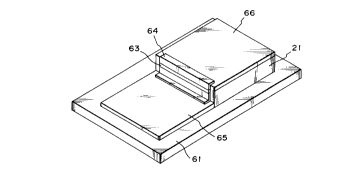
Shown in Figs. 6A, 6B are a substrate ~'1, device
2 S' electrodes 65, 66, and a thin film 64 including an
electron emission portion 63.
-.~ ~1~D3~0
- 26 -
Examples of the substrate 61 are quartz glass,
glass having a reduced impurity content such as of Na,
sodalime glass, a glass substrate obtained by depositing
a layer of Si02, which is formed by a sputtering process
or the like, on sodalime glass, or a ceramic such as
alumina.
Any material may be used for the opposing device
electrodes 65, 66 so long as it is electrically
conductive. Examples that can be mentioned are the
1 0 metals Ni, Cr, Au, Mo, W, Pt, Ti, Al, Cu and Pd or
alloys o.f these metals, printed conductors formed from
the metals Pd, Ag, Au, Ru02, Pd-Ag or from metal oxides
and glass, transparent conductors such as In20g-Sn02 and
semiconductor materials such as polysilicon.
Spacing L1 between the device electrodes is on the
order of several hundred angstroms to several hundred
micrometers. This is decided by the basic
photolithographic technique of the electrode.
manufacturing process, namely the capability.of the
2 0 exposure equipment and the etching process, as well as
by voltage applied across the device electrodes and the
electric field strength capable of producing the
electron emission. Preferably, Ll is on the order of
several micrometers to several tens of micrometers.
2 5 Length W1 and film thickness d of the device
electrodes 65, 66 are selected upon taking into
.-~ 2~.~~3~~
- 27 -
consideration the resistance values of the electrodes
and problems encountered in placing a number of arrayed
electron sources. Ordinarily, the length W1 of the
device electrodes is on the order of several micrometers
$ to several hundred micrometers, and the thickness d of
the device electrodes 65, 66 is on the order of several
hundred 1-lngstroms to several micrometers.
The thin film 64 of the device that includes the
electron emission portion 63 is partly laid on the
device electrodes 65, 66 as seen in Fig. 6B. Another
possible alternative arrangement of the components of
the device will be such that the area of the thin film
64 for preparing an electron-emitting region 63 is
firstly laid on the substrate 61 and then the device
electrodes 65 and 66 are oppositely arranged on the thin
film. Still alternatively, it may be so arranged that
all the areas of the thin film 64 found between the
oppositely arranged device electrodes 65 and.66 operates
as an electron-emitting region 63. The film.thickness
2 0 of the thin film 64 that includes this electron emission
portion preferably is on the order of several angstroms
to several thousand angstroms, with a range of 10
angstroms to 500 angstroms being particularly preferred.
This is selected appropriated depending upon'the step
2 5 coverage to the device electrodes 65, 66, the resistance
values between the electron emission portion 63 and the
2~~~3J0
- 28 -
device electrodes 65, 66, the particle diameter of the
electrically conductive particles constituting the
electron emission portion 63 and the electrification
process conditions. The resistance value of the thin
film indicates a sheet resistance value of from 103 to
107 SZ/
Specific examples of the material constituting the
thin film 64 that includes the electron emission portion
are the metals Pd, Pt, Ru, Ag, Au, Ti, In, Cu, Cr, Fe,
Zn, Sn, Ta, W and Pb, etc., the oxides PdO, Sn02, In203,
Pb0 and Sb203, etc., the borides HfB2, ZrB2, LaB6, CeB6,
YB4 and GdBq, the carbides TiC, ZrC, HfC, TaC, SiC and
WC, etc., the nitrides TiN, ZrN and HfN, etc., the
semiconductors Si, Ge, etc., and fine particles of
1 5 carbon .
The term "a fine particle film" as used herein
refers to a thin film constituted of a large number of
fine particles that may be loosely dispersed, tightly
arranged or mutually and randomly overlapping.(to form
2 0 an island structure under certain conditions).
The electron-emitting region 63 is constituted of a
large number of the fine conductor particles with a mean
particle size of preferably between several'angstroms
and hundreds of several angstroms and most ~sreferably
2 5 between 10 and 200 angstroms.
The electron emission portion 63 comprises a number
2~.~~~~~
which numeral 62 denotes a thin film for forming the
electron emission portion. An example of the thin film
--r
- 29 -
of electrically conductive fine particles having a
particle diameter on the order of several angstroms to
several hundred angstroms, with a range of 10 ~ 500
angstroms being particularly preferred. 'Phis depends
upon the film thickness of the thin film 64 that
includes the electron emission portion and the
manufacturing process, such as the conditions of the
electrification process. The material constituting the
electron emission portion 63 is a substance that is
to partially or completely identical with the devices of
the material constituting the thin film 64 that includes
the electron emission portion.
Various processes for manufacturing the electron-
emitting device having the electron emission portion 63
are conceivable. One example is shown in Fig. 7, in
- SD -
2) The part of the substrate between the device
electrodes 65 and 66 formed thereon is coated with an
organic metal solution, which is then left standing.
The result is formation of an organic thin metal film.
The organic metal solution is a solution of an organic
compound whose principal device is a metal such as the
aforesaid Pd, Ru, Ag, Au, Ti, In, Cu, Cr, Fe, Zn, Sn, .
Ta, w or Pb. Thereafter, the organic thin metal film is ..
subjected to a heating and baking treatment and
patterning is carried out by lift-off or etching to form
the thin film 2 for the electron emission portion [Fig:
7B]. Though formation of the thin film is described as
being performed by application of an organic metal film,
the invention is not limited to this technique.
Formation may be carried out by vacuum deposition,
sputtering, chemical vapor deposition, a dispersive
coating process, a dipping process, a spinner process,
etc.
3) Next, an electrification process referred to as
2 0 "forming" is carried out. Specifically, a voltage is
impressed across the device electrodes 65, 66 in pulsed
form by means of a power supply (not show).
Alternatively, an electrification process based upon
elevating voltage is executed. As a result'bf
2 $ electrification, the electron emission portion 63, the
structure of which has undergone a change, is formed on
~:1~~3~0
_ 31 _
the location of the thin film 62 for forming the
electron emission portion [Fig. 7C]. Owing to the
electrification process, the thin film 62 fox forming
the electron emission portion is locally destroyed,
deformed or changed in property. The resulting region
of changed structure is referred to as the electron
emission portion 63. As described earlier, the
applicants have observed that the electron emission
portion 63 is composed of fine conductive particles.
Fig. 8 illustrates the voltage waveform in a case where
pulses in the forming treatment are applied.
In Fig. 8, T1 and T2 represent the pulse width and
pulse interval, respectively, of the voltage waveform.
The pulse width T1 is on the order of 1 .sec to 10 msec,
the pulse interval T2 is on the order to 10 ,sec to 100
msec, and the crest value of the triangular wave (the
peak voltage at the time of forming) is selected
appropriately. The forming treatment is applied over a
- 32 -
the crest value, pulse width and pulse interval thereof
also are not limited to the values mentioned above.
Desired values may be selected .in accordance with the
resistance value, etc., of the electron-emitting device
so as to form a favorable electron emission portion.
The electric process following forming is carried
out within a measuring apparatus shown in Fig. 9. This
apparatus will now be described.
Fig. 9 is a schematic block diagram of a measuring
apparatus for measuring the electron emission
characteristic of the device having the constitution
illustrated in Figs. 6A and 6B. Shown in Fig. 9 are the
substrate 61, the device-electrodes 65 and 66, and the
thin film 64 for forming the electron emission portion
1~ 63: Further, numeral 91 denotes a power supply for
applying an device voltage Vf to the device, 90 an
ammeter for measuring an devicecurrent If that flows
through the thin film 64 inclusive of the electron
emission portion between the device electrodes_65 and
2 0 ~ 66, 94 an anode electrode for capturing an emission
current Ie emitted by the electron emission portion of
the device, 93 a high-voltage power supply for applying
a voltage to the anode electrode 94, and 92 an ammeter
for measuring the emission current Ie emitted by the
2 5 electron emission portion 63 of the device.
To measure the device current If and emission
~:~~~~~0
- 33 -
current Ie of the electron-emitting device, the power
supply 91 and ammeter 90 are connected to the device
electrodes 65, 66, and the anode electrode 94 to which
the power supply 93 and ammeter 92 are connected is
placed above the electron-emitting device. The
electron-emitting device and anode electrode 94 are
placed inside a vacuum apparatus, which is equipped with
equipment (not shown) such as an exhaust pump and vacuum
gauge and other pieces necessary for vacuum operating
chamber. The device is measured and evaluated in the
desired vacuum.
Measurement is performed at an anode-electrode
~~~o~foo
- 34 -
indicated by Vth in Fig. 7) is applied to the device,
the emission current Ie suddenly increases. When the
applied voltage is less than the threshold voltage Vth,
on the other hand, almost no emission current Ie is
detected. In other words, the device is a non-linear
device having the clearly defined threshold voltage Vth
with respect to the emission current Te.
Second, since the emission current Ie is dependent
upon the device voltage Vf, it is capable of being
controlled by the device voltage Vf.
Third, the emitted electric charge captured by the
anode electrode 94 is dependent upon the time over which
the device voltage Vf is applied. That is, the amount
of electric charge captured by the anode electrode 94 is
capable of being controlled based upon the time over
which the device voltage Vf is applied.
Since the characteristics of the surface-conduction
electron-emitting device set forth above are such that
the device current If and emission current Ie~
2 0 monotonously increase with respect to the applied device
voltage, the electron-emitting device according to the
present invention can be,applied in a wide variety of
ways.
An example of the characteristic in which the
2 5 device current If increases monotonously with respect to
the device voltage Vf tthis is referred to as an MI
- 35 -
characteristic) is indicated by the solid line 1f in
Fig. 10. However, there are also cases in which the
device current if exhibits a voltage-controlled negative
resistance characteristic (referred to as a VCNR
characteristic) with respect to the device voltage Vf
(see the dashed line in Fig. 10). These characteristics
of the.device current are believed to be dependent upon
- 36 -
The substrate 61, the device electrodes 65 and 66,
the thin film 64 that includes the electron emission
portion and the electron emission portion 63 consist of
materials similar to those use in the plane-type
surface-conduction electron-emitting device described
above. The step forming portion 21 and the thin film 64
including the electron emission portion, which
characterize the step-type surface-conduction electron-
emitting device, will now be described in detail.
The step forming portion 21 consists of an
insulative material such as Si02 formed by vacuum '
deposition, printing, sputtering, etc. The thickness of
the step forming portion"21 which corresponds to the
electrode spacing L1 of the plane-type surface-
1$ conduction electron-emitting device described earlier,
is on the order of several hundred angstroms to several
tens of micrometers. The thickness is set depending
upon the manufacturing method of the step forming
portion, the voltage applied across the device
2 0 electrodes and the electric field strength capable of
producing the electron emission. Preferably, the
thickness is on the order, of several thousand angstroms
to several micrometers.
Since the thin film 64 that includes the electron
2 5 emission portion is formed after the device electrodes
65, 66 and step forming portion 21 are fabricated, it is
~~~~~~Q
v
- 37 -
formed on the device electrodes 65, 66. In some cases
the thin film 64 is given a predetermined shape devoid
of an overlapping portion that carries the electrical
connections of the device electrodes 65, 66. Further,
S the film thickness of the thin film 64 that includes the
electron emission portion depends upon the manufacturing
process thereof. There are many cases in which film
thickness at the step portion and film thickness of the
portions formed on the device electrodes 65, 66 differ.
The film thickness at the step portion generally is
less. It should be noted that though the electron
emission portion 63 is shown as being linear on the step
forming portion 21 in Fig. 2, this does not place a
limitation upon its shape and position. The shape and
position are dependent upon the fabrication conditions,
the forming conditions, etc.
Though the basic construction and manufacturing
process of the surface-conduction electron-emitting
device has been described, the scope of the ~,nvention is
2 0 such that the invention is not limited to the foregoing
construction so long as it possesses the three features
described above in connection with the characteristics
of the surface-conduction electron-emitting device. The
surface-conduction electron-emitting device'is
2 S applicable also to wn electron source and an image
forming apparatus such as a display apparatus described
---~ 2~.~0~~0
- 38 -
later.
The electron source and an image forming apparatus
according to the present invention will now be
described.
An electron source or an image forming apparatus
can be constructed by arraying a plurality of the
electron-emitting devices of the invention on a
substrate.
One example of a method of arraying the electron-
emitting devices on the substrate is the ladder array.
Here, as in the prior art, a number of surface-
conduction electron-emitting devices are arrayed in
parallel and both ends of the individual devices are
connected by wiring to form a row of the electron-
emitting devices. A number of these rows are arrayed
along the row direction. Control electrodes (referred
to as a grid) are arranged in the space above the
electron source in a direction (referred to ws the
column direction) perpendicular to the wiring~.of the
rows. This arrangement is called a ladder arrangement
and in this arrangement, the electrons are controlled by
the control electrodes. Another example is referred to
as a simple matrix arrangement. Here n-number of Y-
direction wires are placed upon m-number of,X-direction
2 $ wires via an interlayer insulating layer, and the X- and
Y-direction wires are connected to respective ones of
~~.2~13~~
- 39 -
the pair of device electrodes of each surface-conduction
electron-emitting device. The simple matrix arrangement
will now be described in detail.
A surface-conduction electron-emitting device
according to the present invention has three basic
features in terms of its characteristics.
First, when an device voltage greater than a
certain voltage (referred to as a threshold voltage,
indicated by Vth in Fig. 10) is applied to the device,
the emission current Ie suddenly increases. When the
applied voltage is less than the threshold voltage Vth,
on the other hand, almost no emission current Te is
detected. In other words, the device is a non-linear
device having the clearly defined threshold voltage Vth
with respect to the emission current Ie.
Second, since the emission current Ie is dependent
upon the device voltage. Vf, it is capable of being
controlled by the device voltage Vf.
Third, the emitted electric charge captured by the
2 0 anode electrode 94 is dependent upon the time over which
the device voltage Vf is applied. That is, the amount
of electric charge captured by the anode electrode 94 is
capable of being controlled based upon the time over
which the device voltage Vf is applied.
2 5 In accordance with the foregoing, the electrons
emitted by the surface-conduction electron-emitting
-~ 2'~~~ ~~D
- 40 -
devices, even when they have the form of the simple
matrix array, are controlled by the peak value and width
of a pulsed voltage applied across the opposing device
electrodes at a voltage above the threshold value.
Almost no electrons are emitted at an applied voltage
below the threshold value. In accordance with this
characteristic, surface-conduction electron-emitting
devices can be selected in accordance to an input signal
if a pulse voltage is suitably applied to the individual
to devices even in a case where a number of the devices are
placed in an array. This makes it possible to control
the amount of electron emission.
The construction of an electron-source substrate
produced on the basis of this principle will now be
described with reference to Fig. 11, in which there are
shown an insulative substrate 111, X-direction wiring
112, Y-direction wiring 113, surface-conduction
electron-emitting devices 114 and connections 115. It
should be noted that the surface-conduction electron- _
2 0 emitting devices 114 may be of the plane or step type.
In Fig. 11, the insulative substrata 111 is the
above-mentioned glass substrate or the like, the size
and thickness of which are suitably set depending upon
the number of surface-conduction electron-emitting
2 5 devices placed on the substrate 111, the shape of the
individual devices in terms of design and, if the
~~~~J~~
substrate 111 is a part of a vessel which is constructed
for the purpose of using the devices as an electron
source, the conditions for maintaining the interior of
the vessel in an evacuated state. The X-direction wires
112 comprise m-number of wires Dxl, Dx2. ~~~ Dxm~ These
consist of an electrically conductive metal in desired
patterns formed on the insulative substrate 111 by
vacuum deposition, printing or sputtering, etc. The
material, film thickness and wiring width are set in
such a manner that a substantially uniform voltage will
be supplied to a number of the surface-conduction
electron-emitting devices. The Y-direction wires 113
comprise n-number of wires DY1, DY2, ~~~ Dyn. Like the
X-direction wiring 112, these consist of an electrically
1S conductive metal in desired patterns formed on the
insulative substrate 111 by vacuum deposition, printing
or sputtering, etc. The material, film thickness and
wiring width are set in such a manner that a.
substantially uniform voltage will be supplied to a
2 0 number of the surface-conduction electron-emitting
devices: An interlayer insulating layer (not shown) is
placed between the m-number X-direction wires 112 and n-
number of Y-direction wires 113 to electrically isolate
them and construct matrix wiring (it should'be noted
2 $ that m, n are positive integers).
The interlayer insulating layer (not shown) is a
W ~~~~~~~
- 42 -
material such as Si02 formed by vacuum deposition,
printing or sputtering or the like. The layer is formed
in a desired shape on the entire surface, or on a part
thereof, of the insulative substrate 111 on which the X-
direction wiring 112 has been formed. The film
thickness, material and method of manufacture are
suitably selected so that the insulating layer will be
capable of withstanding the potential difference at the
points of intersection between the X-direction wiring
112 and Y-direction wiring 113. The wires constituting
the X-direction wiring 112 and Y-direction wiring,113
are led out as external terminals.
Further, as set forth earlier, the opposing
electrodes (not shown) of the surface-conduction
electron-emitting devices 114 are electrically connected
by the m-number of X-direction wires 112 and n-number of
Y-direction wires 113 and by the wires 115 comprising an
electrically conductive metal or the like foamed by
vacuum deposition, printing or sputtering, ebG.
2 0 The electrically conductive metal of the m-number
..--
- 43 -
these metals, printed conductors consisting of the
metals Pd, Ag, Au, Ru02, Pd-Ag or metal oxides and
glass, transparent conductors such as In203-Sn02 and
semiconductor materials such as polysilicon. Further,
the surface-conduction electron-emitting devices may be
formed on the insulative substrate 111 or on the
iriterlayer insulating layer, not shown.
More specifically, scanning-signal generating means
(not shown) is electrically connected to the X-direction
wiring 112, as will be described later. The scanning-
signal generating means applies a scanning signal for
scanning, in dependence upon the input signal, the rows
- 94 -
devices can be selected and driven independently merely
by simple matrix wiring.
Current is fed to the device through the above-
described wiring when the aforementioned surface-
conduction electron-emitting devices are formed by the
forming process. However, owing to the problems
mentioned earlier, the voltage applied at the time of
the forming process causes a distribution in the amount
of electron emission of each device owing to a
distribution in the potential drop resulting from the
wiring and heat damage in the wiring. When the surface-
conduction electron-emitting devices are used as an
electron source, it is difficult to obtain a uniform
quantity of electrons with a simple driver. In a case
where the surface-conduction electron-emitting devices
are used as an image forming apparatus, a shortcoming is
that a distribution in luminance occurs.
This problem is solved by using the above-described
process_for forming the plurality of electron-emitting
2 0 devices according to the present invention. preferred
means will be described below for each and every means.
Means A-1 will be described first.
In the electron source having the simple matrix
arrangement of Fig. 11, a potential V2 is applied to all
2 $ wiring terminals DXl to Due, in the X direction, a
potential V1 different from V2 is applied to at least
.. _.,.. .v , ,,... :. .-.: ~..: ~,:",~.z ~~.; °~ .:>:. .,.. ._ :.
...~;. ~~...w :. _..., .:: ,.. ;.,:
:.: ... w
«: . .. , , .. :~..:., . . , : '
.-~ ~~.~~~~o
- 45 -
one arbitrarily selected wiring terminal Dyi in the Y
direction, and the potential V2 is applied to all of the
remaining Y-direction wiring terminals. In accordance
with the present invention, forming is carried out by
applying a voltage of V1-V2 [V] solely to the surface-
conduction electron-emitting devices connected to the
arbitrarily selected Y-direction wiring, and applying a
voltage of V1-V2 = 0 [V) to the other unselected
surface-conduction electron-emitting devices. Forming
1~ is concluded by repeating this process successively.
(This process shall be referred to as "line forming".)
More specifically, the unselected surface-
conduction electron-emitting devices do not attain a
floating state (a state of unstable potential) and the
voltage applied to the devices (while forming is in
progress) is not diverted by the matrix wiring. As a
consequence, the surface-conduction electron-emitting
devices not undergoing the forming treatment.are not
damaged or destroyed by static electricity arnd the
2 0 electron emission portions can be prevented from
deteriorating owing to the influence of the voltage
being applied to the devices undergoing forming, This
makes it possible to obtain uniform characteristics for
each device. ~~
2 5 The aforementioned potentials V1 and V2 are not
necessarily limited to a fixed potential (DC) that does
--, 2~.~~~90
- 46 -
not fluctuate with time. These potentials can be pulsed
waveforms such as triangular or square waves. Further,
both of the potentials V1, V2 may be DC waveforms or
pulsed waveforms or only one may be a pulsed waveform.
At this time the difference voltage V1-V2 (V7 applied to
surface-conduction electron-emitting devices that are to
be subjected to the forming treatment can be supplied as
a voltage waveform sufficient to form the electron
emission portions by the forming treatment. In the case
of a pulsed waveform, the difference voltage V1-V2 [V]
is a peak voltage. Further, a column arbitrarily
selected in order to carry out the forming treatment may
be one column or a plurality of columns simultaneously.
In a case where a plurality of columns are selected, the
temperature distribution within the substrate, which is
caused by the evolution of heat at forming, is taken
into consideration. Accordingly, it is preferred that
the columns be selected in, say, a zigzag manner to
uniformalize the temperature distribution. In a case
2 0 where a plurality of columns are subjected to forming
simultaneously, the time required for forming is
shortened but this requires that the voltage supply have
a large current capacity. Accordingly, in working the
present invention, it is preferred that forming be
2 S carried out by selecting the number of columns giving
the best economical effects upon taking into
_ q~ _
consideration the time required for forming and the
current capacity of the voltage supply.
Furthermore, which of the X- and Y-direction wiring
is selected to perform line farming should be decided in
the manner described below.
Fig. 12 illustrates an equivalent circuit of a
simple-matrix display apparatus using surface-conduction
electron-emitting devices. Here R represents device
resistance and rX, ry represent wiring resistance, in
the horizontal and vertical directions, per pixel.
Further, let NX represent the number of devices in the
horizontal direction and Ny the number of devices in the
vertical direction. When this display apparatus is
subjected to the forming treatment, electric forming
usually is carried out one column at a time or one row
at a time. This so-called "line forming" means carrying
out forming by supplying electric power to a number of
devices from a predetermined power supply portion (one
or a plurality of locations); it does not neoessarily
2 0 mean forming a number of devices simultaneously. Fig.
13 is an equivalent circuit schematically illustrating
line forming. Here the impedance of the wiring, etc.,
outside the apparatus is negligible in comparison with
rz, ry, R. Fig. 13 shows an example in which forming is
2 S carried out collectively in the horizontal direction
(the k-th line from ground). If the device resistance R
48
and wiring resistances rx, ry do not exhibit variance,
the potential division at the devices is such that the
device nearest the power supply portion always is the
highest, as evident from Fig. 13. In addition, the
resistance of a formed device is more than two or three
digits greater that the resistance R prior to the
forming treatment. Accordingly, when line forming is
carried out, devices are electrically formed (=cut off)
successively from the power supply portion side. Fig.
14 is an equivalent circuit for when devices are
electrically formed up to the (n-1)th device and the n-
th device is subjected to forming. More specifically,
in this state also, the ii-th device nearest the power
supply portion is electrically formed and the equivalent
circuit at the next point in time becomes a ladder-
shaped configuration having one less device than in the
circuit of Fig. 14. If a constant voltage vp is applied
to the power supply portion in a state in which devices
up to the (n-1)th device are electrically formed, the
2 0 voltage impressed upon the n-th device will be given by
the following equation:
v (k, n) _ [1-kx ry/R-n x (Nx-n+1) x rX/R] vp ~ (1)
this equation can readily be evaluated as a series
of N-n stages of an ordinary four-terminal matrix. Here
2 5 rX, ry are made sufficiently small in comparison with R.
If this is expressed in terms of power, then the power
.. . '':.~ . ~ ,=. .,,,:;: ~ v : ,: . ,., ~, .. :' : 'a .. ..=..' :: -.
". : ,,: ;: .. :.. ,, ; ;: , ._:
' : _,.. ' :::. . . .' ' .,,:: : ': : : ::' _ ,' . : v;.. , ;,
ti's' .::: ( :, :.:. :. .:..
': ';'. .: ,: ,,., ..,. ..: ,~ .. :: '
applied to the n-th device will be given by the
following equation:
p(k,n) _ [1-2x kx ry/R-2x nx (Nx-n+1)xrx/R]xvpxvp/R (2)
In other words, it may be appreciated that v, p are
functions of k, n and vary as a second degree function
of the device address n in the line-forming direction
and as a first degree function of the device address k
in the other direction. Fig. 15 is a schematic view of
voltage or power distribution within this example.
The line-forming method described above leads to
the following problem: As will be understood from Fig.
15, even if a constant voltage is applied to the power
supply portion, a difference develops, depending upon
the device address, in the voltage and power applied '
when the device is electrically formed. This phenomenon
has a great influence when the number of devices is
large and when the wiring resistance becomes large in
comparison with the device resistance. The~difference
between maximum and minimum, in the n direction, of
power applied immediately before each device is
electrically formed is given by Equation (3) below.
Specifically, maximum power is developed at the power
supply end (n=1) and minimum power is developed at the
central portion (n=Nx/2). If p0 = vpXvp/R,~~ae have
2S p(k,1)-p(k,NX/2) ~ NXxNx/2x(rX/R)xp0 (3)
wherein NX »1.
- 50 -
Further, the difference between maximum and minimum
in the k direction is given by the following equation
since the maximum is developed at the power supply
portion end (k=1) and the minimum is developed at the
ground end (k=Ny).
p(1,n)-p(Ny"n) ~ 2xNyx(ry/R) (4)
wherein Ny »1.
When the number of elements (devices) in the line-
forming direction increases, a difference in the forming
conditions between elements (devices) suddenly develops,
as indicated by the two equations given above.
Accordingly, adverse effects that cannot be ignored
arise when a panel is made for an image forming
apparatus. The example of Fig. l5 is for a case in
(or column). In a case where power supply portions are
at both ends, the power applied immediately before each
which the power supply portion is at one end of the row
device is electrically formed becomes large; owing to
the symmetry of the system, at both ends and~at the
2 ~ central portion of the line (or column) subjected to
line forming, and becomes small in the vicinity of a
length of one-quarter~of the line from both ends. Thus,
a variance occurs depending upon the device address.
In the end, therefore, in a case where~'a simple
~1?~3~0
- 51 -
when a constant voltage vp is applied to the power
supply portion: ,
In order to generalize a method of power supplying
in the embodiment, N' is introduced. The relation N°=N
holds in case of power supplying on one side, and the
relation N°=N/2 holds in case of power supplying on both
sides
p(k,n) - [1-2xkxry/R-2xnx(N'n+1)xrX/R]p0
:P~ = vOxvp/R (5)
Difference between maximum and minimum power in n
direction: 8p = N'x N'/2x(rX/R)xp0 (6)
Difference between maximum and minimum power in k
direction: ,gyp = 2xNyx(ry/R)xp0 (7)
wherein the relation n> Nx/2 is corresponding to n<_
Nx/2 in case of power supplying on both sides.
Furthermore, the same problem occurs also in a case
where the surface-conduction electron-emitting devices
are arrayed in the shape of a one-dimensional ladder
rather than a simple matrix. Figs. 16A, B, and C
2 0 illustrate examples of equivalent circuits and examples
of the difference, due to the device address, in applied
power immediately before each device is electrically
formed in a case where a constant voltage is applied to
the power supply portion.
2 S vet N represent the number of devices, r the wiring
resistance per device and R the device resistance.
- 52 _
Fig. 16A is an example in which the power supply
portion is placed at one location at one end of the
ladder line and the grounded portion is placed at one
location at 'the other end. When a voltage vp is applied
S to the power supply portion, devices are electrically
formed up to the (n-1)th device and the power applied
when the n-th device is electrically formed is a
function of n, as follows:
p(n) - [1+(nxn+n-NxN-3xN-2)x(r/R)]xp0
1 0 ;p0 = v~xv~/R (8)
The difference between maximum and minimum becomes
~p = p(N)-p1 (1) - (N+2)x(N-1)xp0 (9)
Fig. 16B is an exarriple in which the power supply
portion and the grounded portion are placed at one end
1$ on the same side of the ladder line.
Fig. 16C is an example in which the power supply
portions,and the grounded portions are each placed at
..~ ~1203~0
- 53 -
a constant voltage is applied to the power supply
portion, even in the case of a one--dimensional array,
power applied immediately before each device is
electrically formed will develop a variance owing to the
device address.
Accordingly, when an apparatus having surface-
conduction electron-emitting devices in a two-
dimensional array is subjected to electrification
forming one line at a time, good results will be
obtained if forming can be carried out by selecting the
direction (row or column direction) that will reduce the
variance in power applied to each device.
More specifically, this is a forming method for
multiple electron sources characterized in that forming
is carried out in the x direction if the following
holds:
(NyxNX-axNX)xr <_ (NyxNy-axNy)xry (12)
and forming is carried out in the y direction if the -
following holds:
2 0 (NxxNx-axNX)xr > (NyxNy-axNy)xry (13)
where x and y are the two-dimensional directions, NX, Ny
represent the numbers of pixels in the respective
directions and rX, ry.represent the wiring resistances
per device in the respective directions.
2 5 Here a = 8 holds in a case where a power supply
portion is at one end of x or y, and a = 24 holds in a
'"'~. ~~~~~~~
- 54 -
case where power supply portions are at both ends of x
or y. Tt should be noted that the direction is decided
by the power applied when each device is electrically
formed.
S The equations representing the foregoing conditions
will now be described in simple terms.
Since forming by electrification is considered to a
thermal phenomenon, the power applied to each device
represents a problem. Accordingly, the equation set
forth above may be considered as follows
p (k, n) - [1-2XkXr' /R-2xnX (N-n+1) xr/R] xp0
:p0 = vOXv~/R (14)
Tn this case, if the forming is performed in X
.~ ~~~~~~~
- 55 -
of devices on a substrate:
p(1,1)/p0 = 1-2xNxx(rx/R)-2x(ry/R) (16)
Minimum value of the power:
p(Nx/2,Ny)/p0 ~ 1-NXXNx/2X(rx/R)-2XNy(ry/R) (17)
Variance of the power:
,px = fP(1vl)-P(Nx/2,Ny)]Pp ~ (NxxNx/2-
2XNx)X(rx/R)+2XNy(ry/R) (18)
(2) In case of line forming in y direction
p(k,n) - [1-2XnX(rx/R-2Xkx(Ny-k+1)X(ry/R)]Xp0
1 0 ;po = voxvo/R
(19)
Here p becomes maximum when n=k=1 holds and minimum
when n=Nx, k=Ny/2 hold.
Maximum value within surface:
p (1, 1) /p0 = 1-2X (rx/R) -2xNyx (ry/R) (20)
Minimum value within surface:
p~Nx~.Ny/2)/p0 ~ 1-2XNxX(rx/R)-NyXNy/2X(ry/R) t21)
Variance within surface:
Py = LP (1v ~-)-P (NxsNy/2) ]P~ "' 2XNXX(rx/R)'t' (NyxNy/2-
2xNy)x(ry/R) _ , (22)
2 0 Accordingly, if px _< Py holds, i.e., if (NxxNx-
8XNx)xrx <_ (NyxNy-8xNy)xry holds, it is better to perform
forming collectively in the x direction. If px > py
holds, i.e., if (NXxNx-8xNx)Xrx > (NyXNy-BXNy)Xry holds,
it is better to perform forming collectively~in the y
2 5 direction.
In a case where power supply portions are at both
.-\
ends of x or y, as shown in Fig. 17B, the expression of
the condition is as follows if this arrangement is .
considered to be symmetrical with respect to the center
of a line formed collectively:
The condition is set based on whether (NxxNx-
24XNx)Xrx or (NyXNy-24XNy)Xry is larger.
Thus, as set forth above, the direction suited to
line forming is decided by the relationship between the
wiring resistance and number of devices in two
directions.
The voltage waveforms of the forming process.are
similar to those of Fig. 8 and are set in an appropriate
manner.
Means A-2 will now be described.
Forming is carried out upon connecting a forming
power supply (a potential of V1 or V2) to row wiring
(nxi~m) and column wiring (Dyl ~ n) by the arrangement
shown in Fig, l8. At this time V1 is applied to k-
number of the wires among the entirety of row,wires, V2
2 0 is applied to the remaining (m-k)-number of row wires,
V2 is applied to one wire among the entirety of column
wires, and V1 is applied to the remaining (n-1)-number
of the column wires. As a result, kx1+(m-k)x(n-1)-
number of the surface-conduction electron-emitting
2 5 devices among the entirety thereof are selected. In the
selected surface-conduction electron-emitting devices,
- 57 -
the voltage V2-V1 is applied across the device
electrodes 65, 66 of Fig. 6, and electron emission
portions 63, in which there is a change in structure at
parts of the thin film for forming the electron-emitting
devices, are formed.
Next, by interchanging the potentials V1 and V2
connected to the column wiring (or row wiring), the
remaining surface-conduction electron-emitting devices
not selected earlier are selected and forming is carried
out in similar fashion. Waveforms of the kind shown in
Fig. 8 are used as the voltage waveforms of the forming
process.
The difference between this means A-2 and means A-1
is that whereas forming is performed in line units
according to means A-1, here forming is carried out in
block units. The effects are similar to those of A-1.
Specifically, voltage is not diverted to the surface-
conduction electron-emitting devices that have not been
subjected to forming. Further, the number of. devices to
2 0 which the forming voltage is applied is reduced to one
half, as a result of which the value of the current that
flows through the wiring is reduced. As a consequence,
a variance in the characteristics of the surface-
conduction electron-emitting devices owing to a drop in
2 5 the potential of the wiring can be suppressed.
Means B-1 will be described next.
_ ~~zo3~o
The features of the manufacturing process will now
be described with reference to the block diagram of Fig.
19A, the circuit diagram of Fig. 19B and the sectional
view of an individual device of Fig. 19C.
In Fig. 19A, numeral 191 denotes a multiple
electron source, 192 electrical connecting means, 193 a
temperature controller, 194 a forming power supply and
195 a temperature sensor. The portion enclosed by the
solid line represents an electrification treatment
apparatus according to the present invention. The
multiple electron source 191 is an apparatus in which a
plurality of the above-described electron-emitting
devices are arrayed. The devices are connected by
common wiring. The electrical connecting means 192 has
a mechanism for performing an electrical connection at a
plurality of portions of the electron-emitting devices
arrayed in the multiple electron source 191. The
connecting means is connected to each portion of the
multiple electron source via resistors rfl, rf2, as
2 0 shown in Fig. 19B). Since the electrical connecting
means is not restricted in terms of shape (film shape
and size within, one pixel if this apparatus is an image
forming apparatus) such as with regard to the common
wiring of the electron-emitting devices, the'resistances
2 S rfl, rf2 are made sufficiently small in comparison with
the resistance r of the common wiring between devices.
~~.~~3~0
- 59 -
When a connection is made at a plurality of portions of
the electron-emitting devices arrayed in one row and a
voltage is supplied from a power supply VE, as shown in
Fig. 198, the value of a potential drop across the
resistance rf2 is sufficiently small since the number of
parallel wires is small arid the resistance is minute.
The voltage impressed upon the connecting portions to
the common wiring is substantially equal. Further, the
parallel resistances as seen from the junctions are all
equal values since equal numbers of devices on the left
and right axe connected. As a result, the variance in
voltage directly applied to each device can be made very
small in comparison with the case in which
electrification is carried out using the common wiring.
Furthermore, the arrangement is such that a
material having excellent thermal conductivity is used
as connecting mechanisms FC, a component having a large
thermal capacity is provided in the succeeding state,
heating and cooling mechanisms are provided as well as a
2 0 mechanism for controlling them. According to this
arrangement, the connecting mechanisms FC are not only
for passing current through the devices but also act as
conduction paths for heat and function to change the
temperature of the electron emission portions through
2 5 the device electrodes. A schematic sectional view of a
connecting portion is shown in Fig. 19C. Numeral 195
2~~~~~~
- 60 -
denotes a substrate, 65, 65 the device electrodes for
obtaining the electrical connection, 64 the thin film
including the electron emission portion 63, and 197
electrical connecting means.serving as the path for
thermal conduction. Though the electrical connecting
means 197 is shown to be connected on the device
electrodes, it goes without saying that they can be
connected on the wiring.
Examples of the material that can be used to
construct the connecting means 197 are metals such as
aluminum, indium, silver, gold, tungsten and molybdenum
and alloys such as brass and stainless steel. In order
to reduce the contact resistance with respect to the
wiring and suppress a distribution in the contact
1~ resistance at a plurality of contact portions, it is
preferred that the connecting means provided have its
surface, which is a highly rigid metal, coated with a
metal exhibiting a low resistance, and that~each
connecting means be equipped with load applying means
2 0 (not shown) by applying a load in excess of several tens
of grams to the contacting wiring. The load applying
mechanism comprises a resilient member. For example, a
coil spring or leaf spring, etc., may be used.
The above-mentioned electrical connecting means is
2 5 connected to one or a plurality of columns of the matrix
wiring and the forming treatment is applied to one row
2~.~(~~~0
- 61 -
or a plurality of rows simultaneously, after which the
rows connected are shifted so that the forming treatment
is applied to all rows successively) If the number of
electrical connecting means is made large, it is also
possible to form all of them simultaneously.
Furthermore, in a case where the electrical
connecting means is provided on the wiring of the layer
below the insulating layer in the simple matrix
arrangement described above, it is preferred that a
contact window be formed in the contact portion and that
the portion of contact between the wiring of the lower
layer and the electrical connecting means be coated with
a low-resistance metal. "Further, in a combination of
this means with means A-1, satisfactory effects can be
expected by provided the X-direction wiring or x-
direction wiring, namely only the wiring of a row or
column selected in order to apply the forming voltage,
with a plurality of electrical connecting means, and
merely applying a voltage from the terminals~to the
2 0 unselected wiring in the same direction and the wiring
in the other direction.
Though forming means, in an electron source having.a
simple matrix array has been described thus far, it is
possible to utilize means B-1 in an electron source
2 5 having a ladder array as well.
When the forming voltage is applied while the
-1, 2~.~'D~~O
- 62 -
device electrodes are being cooled in the arrangement
described above, the temperature of the film 64 rises
owing to Joule heat produced by the forming current If.
The temperature profile at this time is steep in
S comparison with that of the prior art, in which cooling
is not carried out. The reason for this is that the
heat produced by the devices escapes in a larger amount
from the metal electrodes 65 and 66 than from the quartz
or glass constituting the substrate 67. By cooling the
metal electrodes 65 and 66 through the connecting means
197, the efficiency with which the heat escapes by
conduction is greatly improved.
The inventors have verified that an electron.
emission portion is produced at the peak position of the
temperature profile of the device by the heat of
electrification. The inventors believe that this
temperature is the cause of fissures formation.
Conventionally, the temperature profile. is
broadened when the electrode spacing exceeds.~.0 dim. It
2 0 is believed that the electron emission portion develops
a large variance for this reason. Accordingly, if the
electrode temperature is controlled to be low to make
the temperature profile steep, as is done in this
invention, it becomes possible to make the ~Yariance of
~~.~03~0
- 63 -
In actuality, when forming is carried out while
controlling temperature through the electrification
process of the present invention, the temperature
profile of the film becomes steep and the width of the
S peak region is narrowed, even if the electrode spacing
is made greater than 10 Vim. As a result, the variance
in the electron emission portion is kept small.
Furthermore, it is possible to perform control in
such a manner that each portion of the plurality of
arrayed electron-emitting devices in the above-described
arrangement is kept at a constant temperature. The
aforementioned problem of the prior art, namely the
temperature difference at the central portion and edge
portions of the multiple electron source apparatus, is
1S eliminated. As a result, variance in the electron
emission portions at the time of forming becomes small.
Next, means B-2 will be described.
First, methods of implementation will be described
for an arrangement in which at least one of the row
~.~~~3~~
- 64 -
wiring is fabricated by photolithography or printing.
Tn either case, if the masking pattern is provided with
dividing gaps in advance, wiring having dividing gaps at
predetermined intervals can be obtained with ease. Of
S course, wiring having the gaps at predetermined
intervals may be obtained also by forming continuous
wiring and then severing the wiring by melting it using
a YAG laser or by mechanical means relying upon a dicing
saw.
A method of providing high-impedance portions is as
follows:
A metal having a high resistivity, such as a thin
,,~ 2~.~~~~0
- 65 -
of the wiring. Current may be fed using means similar
to the special electrical connecting means used in means
B-1 described above.
After farming is applied to the predetermined
portions, the dividing gap portions or high-impedance
portions are short-circuited. This method will now be
described.
One method is to achieve the short circuit simply
by using wire bonding or ribbon bonding consisting of Au
1 U or A1.
Another method is as follows: one side of the gap
portion, or the vicinity of the high-impedance portion,
~or part of the high impedance-portion, is coated is
,~ ~~.~Oa~O
- 66 -
According to this method, one row or one column of
devices is subjected to line forming while a voltage
applied to power supply portions is controlled in such a
manner that applied power or applied voltage will be
rendered constant for all devices at the forming of each
device arrayed in a simple matrix, one dimensionally or
in the form of a ladder. In consideratian of the
problem of the prior art, namely the fluctuation in the
voltage supplied to external terminals in order to carry
out forming, line forming is implemented by controlling
the voltage applied to the power supply portions while
sensing up to which device forming has been completed in
a row (or column) undergoing line forming. This makes
it possible to maintain constant forming conditions with
respect to all devices:
In a case where a power supply portion is on one
end of a row (or column) in a two-dimensional simple
matrix array, the voltage applied to the power supply
portion should be made small when forming devices in the
2 0 vicinity of both ends of the row (or column) undergoing
line forming. The voltage applied to the power supply
portion should be made large when forming devices in the
vicinity of the center) Further, in a case where power
supply portions are at both ends of a row (o'r column),
2 5 the voltage applied to the power supply portions should
be made small when forming devices at both ends and in
-~ ~~~f~~~0
- 67 -
the vicinity of the center of the row (or column)
undergoing line forming. The voltage applied to the
power supply portions should be made large when forming
devices in the vicinity of one°quarter of a line inward
from both ends. Further, in a case where one end (or
both ends) of a row (or column) opposing a row (or
column) to undergo line forming is grounded, the voltage
applied to the power supply portions should be made
small if the row (or column) to undergo line forming is
near the grounded end. The applied voltage should be
made large if the above-mentioned row (or column) is far
from the grounded end. -
With regard to a case in which devices are arrayed
in a one-dimensional ladder, if a power supply portion
is placed at one location at one end of the ladder line
and a grounded portion is placed at the other end, then
the voltage applied to the power supply portion is made
small when forming devices in the vicinity of the power
supply end. The voltage applied to the poweW supply
2 0 portion is made large when forming devices in the
vicinity of the grounded end. If a power supply portion
and grounded portion, are placed at an end on, the same
side of a ladder line, then voltage applied to the power
supply portion is made small when forming devices in the
2 5 vicinity of both ends, and voltage applied to the power
supply portion is made large when forming devices~in the
2~.~~~~a
- 68 -
vicinity of the central portion of the line. If pocaer
supply portions and grounded portions are placed at one
location each on both ends of a ladder line, then
voltage applied to the power supply portions is made
small when forming devices in the vicinity of both ends
and in the vicinity of the central portion. The voltage
applied to the power supply portions is made large when
forming devices in the vicinity of one-quarter of a line
inward from both ends.
More specifically, when forming an device at an
device address (k,n) in a simple matrix, for example, in
X direction, it will suffice to apply a voltage va(k,n)
to the power supply portion in accordance with the
equation
1 5 v0 (k, n) = C' X ( 1+kXry/R-l~nX (N-n+1 ) XrX/R] ( 23 )
(where C' is a constant)
to compensate for the voltage distribution of Equation
(1) and attain a constant voltage. Here C'~'decides the
optimum value experimentally. Further, in order to
2 O detect the address of an device that has already
undergone forming, it will suffice to measure the
impedance between the power supply portion and the
grounded portion. The impedance measurement may be
carried out by making one or a plurality of,~forming
2 5 pulses having a fixed pulse height one block, and
inserting a pulse whose voltage is lower than that of
2~~03~~
- 69 -
forming pulses between blocks. An example of pulse
application is shown in Fig. 23. Here T1 is on the
order of 1 ~s ~ 10 msec, and T2 is on the order of 10 ~s
100 msec. Further, N represents 1 ~ 100 pulses, and
S Vi is on the order of 0.1 V.
If the number of blocks (the number of impedance
measurements) is small, the algorithm of forming control
will be simple and the time needed far forming an entire
line can be shortened. If the number of block is large,
to on the other hand, a variance in forming conditions
between devices can be kept small.
It should be noted that the method of applying
forming pulses and the method of detecting device
addresses are not limited to the foregoing. Detection
1$ of device addresses can be dispensed with as long as
fixed conditions are imposed.
Next, with reference to Figs. 24 and 25A, B, an
image forming apparatus used in a display or. the like
that employs an electron source fabricated as, set forth
2 0 above will be described with regard first to a simple
matrix arrangement. Fig. 24 is a basic structural view
showing the image forming apparatus, and Figs. 25A, 25B
show fluorescent films.
Shown in Fig. 24 are an electron-source substrate
2 5 111 on which the electron-emitting devices are
fabricated as set forth above, a rear plate 241 to which
2~~~~~0
- 70 -
the substrate 111 is secured, a face plate 246 having a
phosphor film 244 and a metal back 245 formed on the
inner surface of a glass substrate 243, and a supporting
frame 242. The rear plate 241, supporting frame 242 and
S face plate 246 axe coated with frit glass or the like,
which is then baked in the atmosphere or in a nitrogen
environment at 400 ~ 500°C for more than 10 min to
effect sealing and construct a vessel 248.
In Fig. 24, numeral 247 corresponds to the electron
emission portion in Fig. 1. Numerals 112, 113 denote X-
direction wiring and Y-direction wiring connected.to the
pairs of device electrodes of the surface-conduction
electron-emitting devices. If the device electrodes and
wiring are made of identical material, then are cases in
I5 which the wiring to the device electrodes will be
referred to as device electrodes.
As mentioned above, the vessel 248 is constructed
by the face plate 246, supporting frame 242~and rear
plate 241. However, since the rear plate 241,is
2 0 provided mainly for the purpose of reinforcing the
substrate 111, it may be dispensed with if the substrate
111 itself has sufficient strength. The supporting
frame 242 may be sealed directly on the substrate 111 so
that the vessel 248 may be constructed by the face plate
2 ~ 246,.supporting frame 242 and substrate 111.
Figs. 25A, 25B illustrate the fluorescent film 244.
'~
~1
The fluorescent film 244 comprises only fluoresces if
the apparatus is for monochromatic use. In the case of
a fluorescent film for color, however, the fluorescent
film comprises a black.electrically conductive material
S 251, referred to as black stripes or a black matrix, and
fluoresces 292. The purpose of providing the black
stripes or black matrix is to make color mixing and the
like less conspicuous by blackening the coated portions
between.the fluoresces 252, which are fluoresces of the
three primary colors necessary to present a color
display, and to suppress a decline in contrast caused by
reflection of external light at the fluorescent film
244. As for the material constituting the black
stripes, use can be made of a substance whose principal
ingredient is graphite. I~owever, this does not impose a
restriction upon the invention;. any material may be used
so long as it is electrically conductive and allows but
little light to pass through on to be reflected.
As for the methods of coating the glass~Substrate
2 0 243 with the phosphors, a precipitation method or
printing method irrespective of whether the display is
monochromatic or color:
The inner side of the fluorescent film 244 usually
is provided with the metal back 245. The purpose of the
2 S metal back 245 is to raise luminance by reflecting the
part of the fluorescent light emission that is directed
- 72 -
toward the inner surface to the side of the face plate
246, to act as an electrode for applying an accelerating
voltage to the electron beams, and to protect the
fluorescer against damage due to bombardment of negative
ions generated within the vessel. The metal back is
fabricated by applying a smoothing treatment (usually
referred to as "filming") to the inner surface of the
fluorescent film after the fluorescent film is formed,
and then depositing aluminum (A1) by vacuum deposition.
In order to improve the conductivity of the
fluorescent film 244, there are cases in which the face
plate 246 is provided with transparent electrodes (not
shown) on the side of the outer surface of the film 244.
When the above-mentioned sealing operation is
carried out, it is required that sufficient positioning
be carried out since the color fluorescers of the
various colors and the electron-emitting devices must be
made to correspond in the case of a color display.
The vessel 248 is evacuated to about 10-7 Torr
2 0 through an exhaust pipe (not shown) and then sealed.
There are cases in which a Better treatment is applied
in order to maintain the vacuum after sealing. This is
a treatment in which a Better, which has been disposed
at a predetermined position (not shown) in the vessel
248, is heated by a heating method such as resistive
heating or high-frequency heating immediately before
,.-
~~.~~3~0
- 73 -
sealing is performed or after sealing, thereby forming a
vacuum-deposited film. The principal ingredient of the
Better usually is Ba, etc. By way of example, a vacuum
on the order of 1 x 10⁻⁵ ~ 1 x 10-~ Torr is maintained by
the adsorbing action of the vacuum-deposited film.
In the image display apparatus of the invention
completed as described above, a voltage is applied to
each of the electron-emitting devices through external
terminals Doxi ~ Doxmr Doy1 ~ Doyn. whereby electrons are
emitted. A high voltage Hv greater than several kV is
impressed upon the metal back 245 or transparent
electrodes (not shown). through a high-voltage terminal
Hv, thereby accelerating the electron beams. The
electrons irradiate the fluorescent film 244, thereby
exciting the fluorescer into light emission to display
an image. It should be noted that the external
electrodes Dox1 ~ Doxin. Doyi ~ Doyn of the vessel are
connected to wiring Dxl ~ Dxm, Dyl ~ Dyn, respectively.
The components described above are thosewecessary
2 0 to fabricate a preferred image forming apparatus used in
a display or the like. The particular parts of the
,~ ~~~~~'~3~
- 74 -
An image forming apparatus using an electron source
having the above-described ladder arrangement will now
be described with reference to Fig. 21.
Fig. 21 is a schematic showing the panel structure
S of an image forming apparatus equipped with a multiple
electron source in a ladder array. This differs from
the image forming apparatus of the simple matrix array
described earlier in that grid electrodes are provided
between the electron sources (substrate S) and the face
plate. In other aspects the two apparatuses are
constructed of identical members and are arranged in the
same manner.
Grid electrodes GR (or referred to controlled
electrodes) are provided intermediate the substrate S
1S and face plate FP. The grid electrodes are capable of
modulating the electron beams emitted by the surface-
conduction electron-emitting devices. By way of
example, the grid of Fig. 21 is provided with circular
openings Gh, each of which corresponds to a device, in -
2 0 order to transmit the electron beams to stripe-shaped
electrodes provided perpendicular to the device rows of
the ladder array. The shape of the,grid and the
position at which it is placed need not necessarily be
as shown in Fig. 21. In addition, there are~instances
2 5 win which a number of transmission;holes are provided as
the openings in the farm of a mesh. Further, the gxid
~1?(~~30
_ 75 _
may be provided at the periphery of the surface-
conduction electron-emitting devices or near the
periphery.
The electrodes of the electron source and the grid
electrodes are electrically connected to a control
circuit outside the evacuated vessel.
In the image forming apparatus of the invention,
modulating signals of one line of an image are applied
simultaneously to a row of grid electrodes in
synchronism with successive driving (scanning) of the
device rows one row at a time, thereby controlling the
irradiation of the phosphors with each electron beam and
displaying an image one .Line at a time.
A preferred example of electric circuitry for
1$ carrying out a display operation in which the display
panel created as described above serves as an image
~z~o~~o
- 76 -
register, 225 a line memory, 226 a synchronizing-signal
separating circuit, and 227 a modulating signal
generator. Further, Vx, Va represent DC voltage
sources.
$ The function of each component will be described in
due course. First, the display panel 221 is connected
to external electric circuitry via terminals Dxl ~ Due,
terminals Dyl ~ Dyn and a high-voltage terminal Hue.
Scanning signals for successively driving, one row (N
devices) at a time, the multiple electron-beam sources
provided within the display panel, namely the group of
surface-conduction electron-emitting devices matrix-
wired in the form of an m-row, n-column matrix, are
applied to the terminals DX1 ~ D,~. Modulating signals
for controlling the output electron beams of the
respective devices of the surface-conduction electron-
emitting devices in a row selected by the scanning
signals are applied to the terminals Dy1 ~ Dyn. A DC
voltage of, say l0 KV is supplied to the high=voltage
2 0 terminal Hv from the DC voltage source Va. This DC
voltage is an accelerating voltage for imparting the
electron, beams, which are. delivered by the surface-
conduction electron-emitting devices, with enough energy
to excite the phosphors.
2 5 The scanning circuit 222 will now be described.
The scanning circuit 222 is internally provided
_ 77
with M-number of switching devices (schematically
illustrated by S1 through Sm in Fig. 22). Each
switching device selects either 'the output voltage of
the DC power supply Vx or 0 V (the ground level) and
electrically connects the selected voltage to a
corresponding one of the terminals DX1 through D~ of the
display panel 221. Though the switching devices S1 ~ Sm
operate on the basis of a control signal TSCAN output by
the control circuit 223, in actuality it is possible to
readily realize the switching devices by combining
switching devices such as FETs, by way of example:
In this embodiment, the DC voltage supply Vx has
been set, based upon the characteristic (the electron-
emission threshold voltage) of the surface-conduction
electron-emitting devices, so as to output such a
constant voltage that the driving voltage applied to an
device not being scanned will fall below the electron-
emission threshold voltage. '
On the basis of an image signal that enters from
2 0 the outside, the control circuit 223 acts to coordinate
the operation of each component so as to present an
appropriate display, On.the basis.of a synchronizing ;
signal TSyNC sent from the synchronizing-signal
separating circuit 226 described next, the control
2 5 circuit 223 generates control signals TSCArI. TSFT and
T~qgy to each of the components.
_ 78 _
The synchronizing-signal separating circuit 226
separates a synchronizing signal component and a
luminance signal component from an externally entered
NTSC television signal. If a frequency separating
circuit (filter) is used, the circuit 226 can be readily
constructed, as is well known. Though the synchronizing
signal separated by the synchronizing-signal separating
circuit 226 comprises a vertical synchronizing signal
and a horizontal synchronizing signal, as well known,
here these signals are expressed by the signal TgyNC for
the sake of simplicity. The image luminance signal
component separated from the aforementioned television
signal is represented by a DATA signal for the sake of
simplicity. This signal is applied to the shift
1$ register 224.
The shift register 224 is fox converting the DATA
signal, which enters serially in a time series, into a
parallel signal every line of the image. The shift
register 224 operates based upon the control'signal TgFT
2 0 sent from the control circuit 103. (That is, the
control signal TgFT may be referred to as the shift
clock of the shift register 224.) The serial/parallel-
converted data of one line of the image (which
corresponds to the drive data of N-number of~electron-
2 5 emitting devices) is output from the shift register 224
as N-number of parallel signals ID1 ~ Ipn~
- 79 -
The line memory 105 is a memory apparatus that
stores one line of the image data for a requisite period
of time only. The line memory 105 stores the contents
of ID1 ~ IDn suitably in accordance with the control
signal T MRY sent from the control circuit 223. The
stored contents are output as I'D1 ~ I DN, which enter
the modulating signal generator 227.
The modulating signal generator 227 is a signal
source for appropriately modulating the drive of each of
the surface-conduction electron-emitting devices in
dependence upon individual items of image data I'D1 ~
I'DN. The output signals of the modulating signal
generator 227 are applied to the surface-conduction
electron-emitting devices within the display panel 221
through the terminals D y1 ~ D yn.
As described again, the electron-emitting devices
of the present invention have the following basic
characteristics with respect to the emission current Ie:
Specifically, as mentioned above, the electron emission
has a clearly defined threshold voltage Vth, and an
electron emission is produced only when a voltage
greater than the threshold voltage Vth is applied.
Further, the emission current also changes in
dependence upon a change in the applied voltage of the
devices with regard to a voltage greater than the
electron emission threshold voltage. There are cases in
- 80 -
which the value of the electron-emission threshold
voltage Vth and the degree of change in the emission
current with respect to the applied voltage are changed
by changing the material, construction and method of
manufacture of the electron-emitting devices. In any
case, the following can be said to hold:
Specifically, in a case where a pulsed voltage is
applied to a device, no electron emission takes place
even if a voltage below the electron emission threshold
1~ value is applied. In a case where a voltage greater
than the electron emission threshold value is applied,
however, an electron beam is output. First, it is
possible to control the intensity of the output electron
beam by changing the peak value Vm of the pulse
waveform. Second, it is possible to control the total
amount of electric charge of the output electron beam by
changing the pulse width Pw.
Accordingly, a voltage modulation method and a
pulse-width modulation method can be mentioned as
methods of modulating the electron-emitting devices in
conformity with the input signal. In order to implement
voltage modulation, a circuit used as the modulating
signal generator 227 employs a voltage modulating method
according to which voltage pulses of a fixed~width are
2 5 generated but the peak value of the pulses is suitably
modulated in conformity with the input data.
- 81 -
In order to implement pulse-width modulation, a
circuit used as the modulating signal generator 227
employs a pulse-width modulating method according to
which voltage pulses of a fixed peak value axe generated
but the width of the voltage pulses is suitably
modulated in conformity with the input data.
By virtue of the series of operations described
above, a television display is presented using the
display panel 221. Though not particularly touched upon
above, the shift register 224 and line memory 225 may be
of digital or analog type. What is important is that
the parallel./serial conversion of the image signal and
the storage of the converted signal be performed at a
predetermined speed. In a case where a digital
arrangement is used, it is necessary that output data
DATA of the synchronizing-signal separating circuit 226
be converted to a digital signal. It goes without
saying that this can be readily achieved if'~an A/D
converter is provided at the output of the
2 0 synchronizing-signal separating circuit 226. Further,
it goes without saying that the circuit used as the
modulating signal generator 227 is slightly different
depending upon whether 'the output signal of the line
memory 225 is digital or analog. That is, in case of a
2 5 digital signal, a well-known D/A converting circuit may
be used in the modulating signal generator 22? if
,~ ~~.~~3~D
._ g2 -
modulation is by the voltage modulating method. If
necessary, an amplifier circuit or the like may also be
provided) In a case where modulation is by the pulse-
width modulating method, the modulating signal generator
227 can readily be constructed by one skilled in the art
if use is made of circuit that is a combination of a
high-speed oscillator, a counter for counting the number
of waves output by the oscillator, and a comparator for
comparing 'the output value of the counter with the
output value from the above-mentioned memory. If
necessary, an amplifier circuit may also be provided for
voltage-amplifying the pulse-width modulated signal from
the comparator to the driving voltage of the surface-
conduction electron-emitting devices.
In case of an analog signal, an amplifier circuit
employing a well-known operational amplifier, for
example, may be used in. the modulating signal generator
227 if modulation is by the voltage modulating method.
If necessary, a level-shift circuit or the like may also
2 0 be provided. In a case where modulation is by the
pulse-width modulating method, a well-known voltage-
controlled oscillator (VCQ) may be used. . If necessary,,
an amplifier circuit may also be provided for voltage-
amplifying the pulse-width modulated signal~to the
2 5 driving voltage of the surface-conduction electron-
emitting devices.
''~ ~~~~~~~
- 83 -
Examples of the present invention will now be
described in detail.
[Example 1] '
This example relates to an example of an electron
source in which a number of the surface-conduction
electron-emitting devices fabricated in accordance with
means A-1 are in the form of a simple matrix array.
Fig. 26 is a plan view illustrating a portion of an
electron source. Fig. 27 is a sectional view taken
along line A-A' of Fig. 26. Components in Figs. 26 and
27 that are identical are designated by like reference
characters. Here numeral 261 denotes a substrate, 262
the X-direction wiring (also referred to as "lower
wiring") corresponding to Dx in Fig. 24, and 263 the Y-
direction wiring (also referred to as "upper wiring")
corresponding to Dy in Fig. 24) Numeral 264 denotes a
thin film that includes an electron emission portion.
Numerals 272, 273 denote device electrodes,~'274 an
interlayer insulating-layer, and 275 a contact. hole for
2 0 electrically connecting the device electrode 272 and the
lower wiring 262.
The method of manufacture will now be described in '
detail in accordance s~ith the process steps while
referring to Figs. 28A ~ 28H:
[Step a]
Cr having a thickness of 50 ~ and Au having a
--w
- 84 -
thickness of 6000 A were successively formed by vacuum
deposition on the substrate 261, which was obtained by
forming a film of silicon oxide to a thickness of 0.5 ~.m
on a cleaned plate of sodalime glass 261 by sputtering.
S Thereafter, a photoresist (AZ1370, manufactured by
Hoechst Japan Ztd.) was rotatively applied by a spinner
and then baked. A photomask image was then exposed and
developed to form the resist pattern of the lower wiring
262. The deposited film of Au/Cr was then subjected to
wet etching to form the lower wiring 262 of the desired
shape.
[Step b]
Next, the interlayer insulating layer 274, which
comprises a silicon oxide films having a thickness of
0.1 [Lm, was deposited by RF sputtering.
[Step cl
A photoresist pattern for forming the contact hole
275 in the silicon oxide film, which was depbsited at
- step b; was produced, and the interlayer insulating
2 0 layer 274 was etched away, using the photoresist pattern
as a mask, to form the contact hole 275. The etching
method was RIE (reactive ion etching) using CF4 and H2 ,
gas, by way of example.
[Step dl
2 5 Next, to obtain the device electrodes 272, 273 and
a gap L1 between the device electrodes, a pattern was
85 -
formed by a photoresist (RD-2000N-41, manufactured by
Hitachi Kasei K.K.), after which Ti and Ni were
successively deposited to thicknesses of 50 1~ and 1000
respectively, by vacuum deposition. The photoresist
S pattern was dissolved by an organic solvent and the
deposited film of Ni/Ti was lifted off to form the
device electrodes 272, 273 having the gap L1 between
them. Here the gap was 2 ~.m and the width W1 of the
terminal electrode W1 was 220 ~Lm.
Step e]
After a photoresist for the upper wiring 263 was
formed on the device electrodes 272, 273, Ti and Au were
successively vacuum-deposited to thicknesses of 50P. and
5000 A, respectively. Unnecessary. portions were then
removed by being lifted off to form the upper wiring 263
of the desired shape.
(Step f]
Fig. 29 is a partial plan view showing'a mask of a
thin film 271 for forming the electron emission portion '
2 0 of each surface-conduction electron-emitting device
according to this process. This mask has the gap L1
between the device electrodes and openings in the
vicinity thereof. By using this mask, a Cr film having
a film thickness of 1000 A was deposited by~vacuum
2 5 deposition and subjected to patterning. Organic Pd
(CCP4230, manufactured by Okuno Seiyaku K.K.) was then
--~ ~~.~~~~0
- 86 -
rotatively applied to the Cr thin film by a spinner,
after which a heating and baking treatment was applied
for 10 min at 300°C. The thus formed thin film, which
is for forming the electron-emitting device, comprising
S fine particles the principle device of which was Pd had
a film thickness of 100 A. The sheet resistance value
was 5 ~ 104 SZ/ . The film of fine particles is a film
constituted of a large number of fine particles, as set
forth earlier. As for the fine structure, the fine
particles are not limited to loosely dispersed
particles; the film may be one in which the fine
particles are tightly arranged or mutually and randomly
overlapping (to form an island structure under certain
conditions). The fine particles have a mean particle '
1S size of preferably between several angstroms and
hundreds of several angstroms.
LStep g1
g7 _
angstroms, respectively, by vacuum deposition. By
removing unnecessary portions of the photoresist by
lift-off, the contact hole 275 was left filled.
Thus, by performing the foregoing process, the
S lower wiring 262, the interlayer insulating layer 274,
the upper wiring 263, the device electrodes 272, 273 and
the thin film 277 for forming the electron emission
portion were formed on the same insulative substrate
261. The substrate fabricated as set forth above is
referred to as an electron-source substrate that has not
been subjected to forming.
Next, a detailed example will be described in
which, using the electron-source substrate that has not
been subjected to the forming treatment, an electron
1S source is fabricated by carrying out the forming
treatment according to the present invention.
Fig. 30 is a diagram for describing this embodiment
and shows the electrical connections when foaming is
applied to part of a group of surface-conduct$on
2 0 electron-emitting devices wired in the form of a simple
matrix in the manner described earlier. For the sake of
convenience, only 6 x 6 surface-conduction-electron-
emitting devices are shown to be wired in the form of
the simple matrix. According to this embodiment,
2 S however, a 300 x 200 matrix has been fabricated.
In order to distinguish among the surface-
2~~D390
conduction electron-emitting devices in the description,
the devices are represented by (X,Y) coordinates in the
form D(1,1), D(1,2), ~~~, D(6,6) iri Fig. 30.
Further, Dxl r Dx2 r ~ . , r Dx5 and Dyl, Dy2, ~ . . , Dys in
Fig. 30 represent the respective wires of the simple
matrix wiring. These wires electrically connect the
matrix to the outside via terminals P.
Further, VE represents a voltage source having the
capability to generate a voltage necessary for the
forming of the surface-conduction electron-emitting
devices.
Fig) 30 illustrates a voltage application method
for simultaneously forming 300 devices, namely D(1,3),
D(2,3), D(3,3), D(4,3), D(5,3), D(6,3), -~ ~, D(300,3) .
As shown in Fig. 30, ground level, namely 0 V, is
applied to the wire Dx3. A potential of, say, 6 V from
a voltage source Vform is applied to the X-direction
wiring other than wire Dxg, namely to wires,Dxl, Dx2r
Dx4r DxSr Dx6. °~°, Dx2Op) At the same time, ,a potential
2 0 from the voltage source Vgprm is applied to each of the
wires D~,lr Dy2r Dy4r DySr Dy6r ~ "s Dy300~
As a result, the output voltage of the voltage
source Vform is impressed across the devices D(1,3),
D(2,3), D(3,3), D(4,3), D(5,3), D(6,3). ° ° °;' D(300,3)
2 5 that have been selected from among the plurality of
matrix-wired devices. Consequently, these 300 devices
'~1
- 89 -
are subjected to forming in parallel.
As for the devices other than the above-mentioned
300 devices, a substantially equal potential (the output
potential of the voltage source VE) is applied to both
ends of each device, so that the voltage across each
device is approximately 0 V. Naturally, this means that
these devices are not subjected to forming. The thin
film comprising the electron emission material does not
deteriorate and is not damaged.
1D The electron emission portions thus fabricated
consisted of fine particles, the principle ingredient of
which was palladium, in a dispersed state. The average
particle diameter of the particles was 30 angstroms.
The resistance of each device was about 1 kS2, the
resistance (in the x direction) of the lower wiring per
device was about 0.03 SB, and the resistance (in the y
' direction) of the lower wiring per device was about 0.1
S2 . , .
In a case where the power supply portion is on one
2 0 side, we have the following from Equation (12), as set
forth earlier: .
(NxXNx-8N~)Xrx = 262$, (NyXNy-8Ny)Xry = 3840
Therefore, though the number of devices is large, the
devices in the x direction should be subjected to
2 5 forming.
In order to ascertain the characteristics of a
--, 212~J3~~?
- 90 -
number of plane-type surface-conduction electron-
emitting devices fabricated by the foregoing process,
the electron emission characteristics were measured
using the measuring apparatus of Fig.9.
$ As for the measurement conditions, the distance
between the anode electrode and the surface-conduction
electron-emitting device was made 4 mm, the potential of
the anode electrode was made 1 kV, and the degree of
vacuum within the evacuated vessel at the time of
measurement of the electron emission characteristic was
set at 1 x 10⁻⁶ Torr.
In a typical surface-conduction electron-emitting
device in this embodiment, emission current Ie increased
sharply from an device voltage of 8 V. At an device
voltage of 14 V, device current If was 2.2 mA, and the
emission current Ie was 1.1 plA. Electron emission
efficiency = Ie/If (o) was 0.050.
According to this embodiment, the variance in
electron emission efficiency was less than 74,for all
2 0 devices, indicating that substantially uniform
characteristics were obtained.
(Example 2)
Here an example will be described in which an image
forming apparatus was constructed using the~~electron-
2 S source substrate, fabricated according to Example l,
that has not been subjected to the forming treatment.
_~., 21?~~~Q
_ 91 -
This will be described with reference to Figs. 24 and
25A, 25B.
The electron-source substrate 111, obtained by
arranging 300 x 200 devices, which have not been
subjected to the aforementioned forming treatment, was
secured to the rear plate 241, after which the face
plate 246 (comprising the phosphor film 244, which is an
image forming member, and the metal back 245 on the
inner surface of the glass plate substrate 243) was
disposed 5 mm above electron-source substrate 111 via
the supporting frame 242, and the joints of the face
plate 246, supporting frame 242 and rear plate 241 were
coated with frit glass, which was then baked in the
atmosphere at 400'C for 10 min to effect sealing.
1$ Fixing of the electron-source substrate 111 to the rear
plate 241 was also accomplished by using frit glass.
The fluorescent film 244 comprises only fluorescer
if the apparatus is for monochromatic use. .In this
embodiment, however, the fluorescent film 244.,was
2 0 fabricated by forming black stripes (as shown in Fig.
25) in advance and applying a coating of various color
phosphors between the stripes. As for the material
constituting the black stripes, use was made of a
substance whose principal ingredient was graphite. The
2 5 slurry method was used to coat the glass substrate 244
with the phosphors.
.,~ ~~~o~oo
The metal back 246 provided on the inner side of
the fluorescent film 245 was fabricated by applying a
smoothing treatment (usually referred to as "filming")
to the inner surface of the fluorescent film after the
fluorescent film was fabricated, and then depositing A1
by vacuum deposition. In order to improve the
conductivity of the fluorescent film 245, there are
cases in which the face plate is provided with
transparent electrodes on the side of the outer surface
of the film 245. In this embodiment, however, the
electrodes were not used since satisfactory conductivity
was obtained with the metal back 246 alone. When the
above-described sealing operation is performed,
sufficient positioning is carried out since the color
fluorescer and the surface-conduction electron-emitting
devices must be made to correspond in the case of a
color display.
The environment within the glass vessel. completed
as described above was withdrawn through an exhaust pipe
2 0 (not shown) using a vacuum pump. After a degree of
vacuum on the order of 10'5 Torr was attained, a voltage
was applied across the device electrodes through
external terminals,DOX1 ~ DOXm~ DOY1 ~ DOYn according to
the scope of Example 2, whereby the above-described
2 5 electrification treatment (forming treatment) was
applied to form the electron emission portions and
~~~Q3~p
fabricate the surface-conduction electron-emitting
devices.
Next, the exhaust pipe (not shown) was heated by a
gas burner in a vacuum on the order of 1 x 10'6 Torr,
thereby sealing off the vessel by fusing it.
Finally, a Better treatment was applied in order to
maintain the vacuum after sealing. Specifically, a
Better of Ba, which was disposed at a predetermined
position (not shown) in the image forming apparatus, was
heated by a high-frequency heating method after the ..
sealing treatment, thereby forming a vacuum-deposited
film.
In the image forming apparatus of the invention
completed as described above, scanning signals and
modulating signals were applied to each of the surface°
conduction electron-emitting devices through the
external terminals Dpgl ~ Dpi, Dpyl ~ Doyn by signal
generating means (not shown), whereby electrons were
emitted. A high voltage greater than several, kilovolts
2 0 was impressed upon the metal back 245 through the high-
voltage terminal Hv, thereby accelerating the electron
beam. The electrons were thus caused to bombard the
fluorescent film 244, thereby exciting the fluorescer
into light emission to display an image.
2 5 In the image forming apparatus fabricated according
to this Example, it was confirmed that the device
2:~~D~~O
characteristics were uniform and that a great
improvement was achieved in the uniformity of the
luminance of the display image owing to the fact that a
number of surface-conduction electron-emitting devices
wired in the form of a simple matrix could be formed
uniformly.
In actuality, two display apparatuses fabricated as
described above were prepared. In one apparatus, the
power supply portion was provided on one side only and
line forming was carried out in the x direction. In the
other apparatus, the power supply portion was provided
on one side only and line forming was carried out in the
y direction. A cons~tant-voltage was applied to each
pixel, 5 kV was applied to the high-voltage terminal Hv
and luminance was measured. Whereas line forming in the
x direction resulted in luminance irregularity of less
than 70, line forming in the y direction resulted in
luminance irregularity of 150. In other words, it will
be understood that the direction in which line forming
2 0 should be carried out can be decided prior to forming.
(Example 3)
Described next will be an image forming apparatus
fabricated in the same manner as in the Example 2 using
means A-1 according to the present invention. Tn this
2 S example, however, the number of devices, the shape of
- 95 -
Example 2. An electron-source substrate was fabricated
in which NX = 50, rX = 0.3 3Z, Np = 50, ry = .1 S2, R = 1
kS2, using the expressions already described. Further,
the image forming apparatus had a structure in which
S current could be fed from both ends of the wiring in the
X,and Y directions.
In a case where power supply portions are provided
on both sides of each wire, we have the following, as
described earlier:
1 ~ (NXXNx-24NX) XrX = 39, (NyXNy-24Np) Xrp = 18
That is, it will be appreciated that the surface-
conduction electron-emitting devices in the Y direction
should be subjected to forming.
As in the Example 2, two panels subjected to the
15 forming treatment by two methods, namely the line
forming method in the x direction and the line forming
method in the y direction, were compared. It was found
that luminance irregularity bras 12% with the.former and
less than 6o with the latter. Clearly, carrying out the
2 ~ forming treatment in the y direction gives less
luminance irregularity. 2n other words, it will be
understood that the direction in which line forming
should be carried out can be decided prior to forming.
(Example 4)
2 5 A treating apparatus for carrying out the forming
treatment of means A-1 according to the present
,. ... : . ' .:: ..~. .. - ::. .°. ; .;. -:.: ~ : ~» .. . ~. ; . . . :
: . :;
2~.~~ a~0
_ 96 _
invention will now be described.
Fig. 31 shows an example of an electric circuit
arrangement of a forming treating apparatus. Numeral
311 in Fig. 31 denotes an electron°source substrate,
which has not been subjected to the forming treatment,
obtained by wiring, in the form of a simple matrix, m x
n surface-conduction electron-emitting devices
fabricated through a process similar to that of Example
1. Numeral 312 denotes a switching device array, 313 a
forming pulse generator, and 314 a control circuit.
The electron-source substrate 311 is electrically
connected to the peripheral electric circuitry via
terminals Dx1 ~ Dxn, Dyl w Dyn. The terminals Dxl ~ D~
are connected to the switching device array 312, and the
terminals Dyl a Dyn, are connected to the output of the
forming pulse generator 313.
The switching device array 312 is internally
equipped with n-number of switching devices..Sl ~ Sn.
The switching devices function to connect respective
---~ 2~.~~3~0
97 _
a circuit for controlling the operation of the switching
devices and the operation of the forming pulse generator
313, as described above. ,.
The functions of the various components are as
described above. Overall operation will now be
described.
First, before forming is started, all of the
switching devices of the switching device array 312 are
connected to the ground-level side in response to
control by the control circuit 314. Further, the output
voltage of the forming pulse generator 313 also is held
at the ground level of 0 V.
Next, in order to select one row of the device rows
and subject them to the forming treatment, as described
in connection with Fig. 30, the control circuit 314
generates the control signal SC1 in such a manner that
all of the switching devices in the switching device
array 312 other than those connected to the~.row to
undergo the forming treatment will be connected to the
2 0 side of the forming pulse generator 313. (In the
example illustrated in Fig. 31, all switching devices
excluding S3 are connected to the side of the forming ,
pulse generator 313).
Next, the control circuit 314 sends the forming
2 $ pulse generator 313 the control signal SC2, in response
to which the generator 313 generates voltage pulses
~:~?~390
--~1
9$ _
suitable for forming.
If forming for the selected row of devices is
completed, the control circuit 314 generates the control
signal SC2, causing the forming pulse generator 313 to
halt pulse generation and sending the output voltage to
O.V. Furthermore, the control signal 314 generates the
control signal SC1 so that all of the switching devices
contained in the switching device array 313 will be
connected to the side of the ground level.
By virtue of the foregoing operational procedure,
forming of the arbitrarily selected row of devices is
completed. By successively forming other rows of
devices by a similar procedure, it is possible to
.~ 2~.~~~~0
- 99 -
measure a typical device in a fabricated electron
source, it was found that emission current Ie increased
sharply from an device voltage of 8 V. Further, at an
device voltage of 14 V, device current If was 2.4 mA,
and the emission current Ie was 1.0 ~t.A. Electron
emission efficiency '~= Ie/If ( o) was 0.04.
When a variance in fissure formation occurs, the
above-described uniformity of electron emission
efficiency between devices is not obtained. However, in
accordance with the forming apparatus of the present
invention, the variance in voltage effectively applied'
to each device becomes small at the instant forming is
carried out, and the variance in electron emission
efficiency between devices is held below 10o as an
device characteristic.
(Example 5)
Next, a specific example will be described in which
an electron source is produced by carrying out the
forming treatment based upon the aforesaid means A-2
2 0 using an electron-source substrate, identical with that
fabricated in Example l, which has not been subjected to
the forming treatment.
Fig< 18 is a diagram for describing this embodiment
and shows the electrical connections when fb~ming is
2 S applied to part of a group of surface-conduction
electron-emitting devices wired in the form of a simple
~~~D3~D
- 100 -
matrix in the manner described earlier.
According to the arrangement of Fig. 18, forming is
carried out by connecting a forming power supply (a
potential of V1 or V2) to row wiring (Dxl~m) and column
wiring (Dyl ~ n). At this time the potential V1 is
applied to k-number of the wires among the entirety of
row wires, the potential V2 is applied to the remaining
(m-k)-number of row wires, the potential V2 is applied
to L-number of wires among the entirety of column wires,
and the potential V1 is applied to the remaining (n-L)-
number of the column wires. As a result, KXL+(m-K)x(n-
L)-number of the surface-conduction electron-emitting
devices among the entirety thereof are selected. A
voltage of substantially V2-V1 (6 V in this embodiment)
is applied to the selected surface-conduction electron-
emitting devices to carry out forming.
As for the devices other than the above-mentioned
selected devices, a substantially equal potential is
applied to the electrodes at both_ends of the, devices,
2 0 so that the voltage across each device is approximately
0 V. Naturally, this means that these devices are riot
subjected to forming. In addition, the thin film for
forming the electron emission portions does not
deteriorate and is not damaged. ,
2 5 Next, by interchanging the potentials V1 and V2
connected to the column wiring (or row wiring), the
.--~
- 101 -
remaining surface-conduction electron-emitting devices
not selected earlier are selected and forming is carried
out in similar fashion.
In order to ascertain the characteristics of the
number of surface-conduction electran-emitting devices
fabricated in the foregoing process with m, n set at
100, K and I. set at 50, the electron emission
characteristics were measured using the measuring
apparatus of Fig.9.
As for the measurement conditions, the distance
between the anode electrode and the surface-conduction
electron-emitting device was made 4 mm, the potential of
the anode electrode was made 1 kV, and the degree of
vacuum within the evacuated vessel at the time of
measurement of the electron emission characteristic was
set at 1 x 10-s Torr, as in the above-described example.
As a result, the electron emission efficiency 'r, = Ie%If
(o) was 0.040. Further, substantially uniform
characteristics were obtained for all devices.. For
2 0 example, variance in the electron emissian efficiency
was less than 80 overall.
tExample 6)
An image forming apparatus fabricated by applying a
forming treatment identical with that of Example 5 will
2 5 now be described with reference to Fig. 24.
Though the arrangement and method of fabrication
2~~~~9~
- 102 -
are similar to those of Example 2 described earlier,
here an image forming apparatus that has not been
subjected to the electrification treatment is fabricated
using an electron-source substrate on which 100 x 100
$ devices are wired in the form of a simple matrix, i.e.,
a substrate identical with that fabricated in Example 5.
The environment within the glass vessel completed
as described above was withdrawn through the exhaust
pipe (not shown). After a degree of vacuum on the order
of 1 x 10⁻⁵ Torr was attained, a voltage was applied
across the device electrodes through external terminals
Doxl ~ Doxm~ DOY1 ~ DoYn according to the scope of Example
5, whereby the above-described electrification treatment
(forming treatment) was applied to form the electron-
emitting devices and fabricate the surface-conduction
electron-emitting devices.
Next, the exhaust pipe (not shown) was heated by a
gas burner in a vacuum on the order of 1 x 10'6 Torr,
thereby sealing off the vessel by fusing it.~~
2 0 Finally, a Better treatment was applied in order to
maintain the vacuum after sealing.
Tn the image forming apparatus of the invention
completed as described above, scanning signals and
modulating signals were applied to each of ~~e surface-
2 5 conduction electron-emitting devices through the
external terminals Doxl ~ Dog, Dpyl ~ DoYn by signal
- 103 -
generating means (not shown), whereby electrons were
emitted. A high voltage was applied through the high-
voltage terminal Hv to display an image.
In the image forming apparatus fabricated according
to this Example, it was confirmed that the device
characteristics were uniform and that luminance
irregularity of the displayed image was less than 8~
owing to the fact that a number of surface-conduction
electron-emitting devices wired in the form of a simple
matrix could be formed uniformly.
(Example 7)
Described next will be an electron source
fabricated by carrying aut the forming treatment
according to another method based upon means A-2 of the
invention using the electron-source substrate, which has
not been subjected to the forming treatment, fabricated
according to Example 1.
Fig. 33 illustrates the electrical connections when
forming is carried out with regard to half the number of
2 0 a group of 640 x 400 surface-conduction electron-
emitting devices, which have not been subjected to the
forming treatment, wired in a simple matrix array.
In Fig. 33, Dxl, Dx2, ~.~, Dx400 and Dyl, Dy2, ...~
D~'640 represent the individual wires of the'simple
2 5 matrix wiring. Further, V1, V2 denote power supplied
for generating forming pulses.
.~ ~~.~fl~flfl
- 104 -
Fig. 33 illustrates a voltage application method
for a case where the devices indicated in black are
subjected to selective forming. Specifically, Vl is
ground level and V2 is a potential Vfo~. A voltage of
approximately V2-V1, namely Vform, is applied across both
end of the black devices, and approximately 0 V is
applied across the white devices. As a result, the ..
black devices undergo forming selectively and the white
devices are unchanged.
1~ Fig. 34 illustrates an electric circuit arrangement
for carrying out the forming treatment by the above-
described method. Numeral 341 denotes a substrate of an
electron source obtained by wiring, in the form of a
simple matrix, 640 x 400 surface-conduction electron-
emitting devices that have not been subjected to the
forming treatment. Numeral 342 denotes.a switching
circuit, 343 a forming pulse generator and 344 a control
circuit.
Of the row wires (Dxl, Dx2r ' ' ~ Dx400) ~ ~~he odd-
2 0 numbered groups are connected to ground level and the
even-numbered groups are connected to the output of the
forming pulse generator 343. Of the column wires (Dyl,
Dy2. " '. Dy640). the odd-numbered groups are connected
to ground level or to the output of the form~.ng pulse
2 5 generator and the even-numbered groups are connected to
ground level or to the output of the formingpulse
~'~.~~390
- 105 -
generator. However, the column wires are not all
connected to the forming pulse generator simultaneously.
The switching circuit 342 changes over the
connections of the column wires in response to a signal
from the control circuit 344. The forming pulse
generator 343 outputs the forming pulses in accordance
with a control signal generated by the control circuit
344.
First, prior to the start of forming, all wires are
1 0 held at ground level. Next, the control circuit 344
sends a signal to the switching circuit 342 so as to
connect the odd-numbered groups of the column wires to
the output of the timing pulse generator 343 and
connected the even-numbered groups of the column wires
to ground level. The control circuit 344 then sends a
signal to the forming pulse generator 393 so that
forming is carried out. The forming pulses are applied
to the selected surface-conduction electron-emitting
devices. At this time a forming current for~320
2 O devices, which is half the 640 surface-conduction
electron-emitting devices in the row direction, flows
into each row wire, and current for 200 devices
similarly flows into each column wire.
When the forming of all'selected devices is
2 5 completed, the switching circuit 342 is changed over to
connect the odd-numbered column wires to ground level
e~
- 106 -
and the even-numbered column wires to the output of the
timing pulse generator 3~3, whereby the remaining
devices are selected so that the forming pulses may be
applied and forming carried out in a similar manner.
In 'this Example, pulses having a voltage waveform
of the kind shown in Fig. 8 were applied to the selected
devices and the electric forming treatment was performed
in accordance with the procedure set forth above.
Furthermore, in this Example, pulse width T1 was 1 msec,
pulse interval T2 was 10 msec, the peak value of the
triangular waveform (the peak voltage at the time.of
forming) was 5 V, and the forming treatment was carried
out for 60 sec under a vacuum of about 1 x 10⁻⁶ Torr.
In this Example, a temperature rise due to the
1$ current that flows into each wire at forming time could
be suppressed and there was no damage to the wiring or
substrate whatsoever. Furthermore, since a number of
the matrix-wired surface-conduction electron-emitting
devices were formed in staggered fashion, as~,shown in
2 0 Fig. 33, a temperature irregularity did not develop and
forming could be carried out in excellent fashion.
As a result, as in Example 5, measuring the
electron emission characteristics showed that the
electron emission efficiency 'i'~ = Ie/If (~a 3~as 0.05.
2 5 Further, substantially uniform characteristics were
obtained for all devices. For example, variance in the
~~2~~~D
- 107 -
electron emission efficiency ~ was less than 13~
overall.
Further, with respect to the image forming
apparatus, prior to the forming treatment, fabricated
with an arrangement similar to that of Example 6, a
number of surface-conduction electron-emitting devices
wired in the form of a simple matrix could be formed
uniformly also in the image forming apparatus fabricated
by applying the forming treatment according to the
method of this Example. As a result, it was confirmed
that the device characteristics were uniform and that
the luminance irregularity of the displayed image was
less than 130.
(Example 8)
Examples 1 through 7 relate to a method of
supplying current through wiring from external terminals
so as to apply a forming voltage to only some of the
devices. In this example, however, current~'is supplied
to devices by the aforesaid means B-1 using electrical -
2 0 connecting means other than wiring.
The method used in this Example can be implemented
.,.~
- 108 -
devices are connected in the ladder array will be
described with reference to Fig. 65.
A thin film of Ni having a thickness of 1000
angstroms was formed by vacuum deposition on a substrate
651 obtained by forming a film of silicon oxide to a
thickness of 0.5 N,m on a cleaned sheet of blue glass by
means of sputtering. Device electrodes 655, 656 were
then formed by photolithography.
A Cr film having a film thickness of 1000 angstroms
was deposited by vacuum deposition and subjected to
patterning by photolithography using a mask (Fig. 29)
having the inter-device electrode gap L1 and an openings
in the vicinity thereof... Organic Pd (CCP4230,
n
- 109 -
feature of the present invention. Numeral 351 denotes a
surface-conduction electron-emitting device, 1000 of
which are arrayed in parallel. Numeral 352 denotes an
Ni electrode, which serves as common wiring for passing
S current through each of the devices. Needle-shaped
cppper terminals 353 serve as terminals for achieving
electrical connection at a plurality of portions of the
common wiring 252. Bulk wiring 354 made of copper
electrically connects the copper terminals 353 and a
forming power supply. The above-mentioned copper
terminals are so arranged as to be connected in 332 sets
every three surface-conduction electron-emitting
devices. The copper terminals are.contact-bonded to the
common wiring 352 and a voltage necessary for the
forming of devices is applied to the common wiring 352
from the forming power supply to form fissures that
~~~~Q~a
- 110 -
invention, the variance in the voltage at the portions
in contact with the copper terminals (353 in Fig. 35)
was held to less than 0.001 V. Variance in the electron
emission efficiency between devices was held to less
than 5o as an actual characteristic of the devices.
(Example ~)
Here an example will be described in which an image
forming apparatus was constructed using the electron-
source substrate, fabricated through a process the same
as that of Example 8, that has not been subjected to the
forming treatment. This will be described with
reference to Figs. 21 and 60.
First, a forming treatment using electrical
connecting means was performed in a nitrogen environment
in the same manner as in Example 8, and the substrate
was fixed to the rear plate.
Fig. 21 is a schematic showing the panel structure'
of an image forming apparatus equipped with,a multiple
electron.source in a ladder array. In Fig. 2~, VC
2 0 represents a vacuum vessel made of glass, a portion FP
of which is a face plate on the front surface side.
Transparent electrodes made of ITO, for example, are
formed on the inner surface of the face plate FP, and
the transparent electrodes are coated with f~luorescer
2 5 for red, green and blue in a mosaic pattern or striped
pattern. In order to avoid a complicated diagram, the
2~.~(~3~(D
- 111 -
transparent electrodes and fluoresces axe represented
collectively by P~3 in Fig. 21.
A black matrix or black stripes well known in the
CRT field may be provided between the fluoresces of each
color, and it is also possible to form a well-known
metal back layer on the fluoresces. The above-mentioned
transparent electrodes are electrically connected to the
outside of the vacuum vessel through a terminal EV so
that an electron-beam accelerating voltage can be
applied. In this Example, a high voltage of 4 kV was
applied.
The rear plate S is the substrate of the multiple
electron beam source and.is secured to the bottom of the
vacuum vessel VC. Surface-conduction electron-emitting
devices are formed and arrayed on the substrate in the
manner described above. In this Example, 200 device
rows are provided, in each of which 200 devices are
wired iri parallel. The two wiring electrodes of each
device row are connected alternately to electrode
2 0 terminals Dpl ~ Dp200 and Dml ~ D~00, which are provided
on respective side faces of the~panel. Thus, electric
driving signals can be applied from outside the vessel.
Further, grid electrodes GR in the form of stripes.
are provided intermediate the rear plate S and the face
2 5 plate FP. The grid electrodes GR are .200 independent
electrodes pravided perpendicular to the device rows
--~ 2 .~. 2 0 ~ ~ 0
- 112 -
(i.e., in the Y direction). Each grid electrode is
provided with an opening Gh through which an electron
beam is transmitted. The holes Gh are circular and each
is provided to correspond to one of the surface-
s conduction electron-emitting devices. In certain cases,
however, a number of them may be provided in the form of
a mesh. The grid electrodes are electrically connected
. with the outside of the vessel by electrode terminals G1
"' 6200~ As long as the grid electrodes are capable of
modulating the electron beams emitted by the surface-
conduction electron-emitting devices, the shape at. the
positions at which they are placed need not necessarily
be as shown in Fig. 21. For example, the grid
electrodes may be provided at the periphery of the
surface-conduction electron-emitting devices or near the
periphery.
In this display panel, ~a 200 x 200 XY matrix is '
constructed by the device rows of,the surface-conduction
electron-emitting devices and the grid electrodes.
2 0 Accordingly, by simultaneously applying modulating
signals for one line of an image to a grid electrode row
in synchronism with successively row-by-row drive
(scanning) of the device rows, irradiation of the
phosphors with each electron beam is controlled to
2 5 display the image line by line.
Fig. 53 is a block diagram illustrating an electric
2~~~3~0
- 113 -
circuit for driving the display panel of Fig. 21. Shown
in Fig. 53 are the display panel of Fig. 21, indicated
at number 600, a decoding circuit 601 for decoding a
composite image signal that enters from the outside, a
serial/parallel converting circuit 602, a line memory
603, a modulating signal generating circuit 604, a
timing control circuit 605 and a scanning signal
generating circuit 606. The electrode terminals of the
display panel 600 are connected to various electric
circuits. The terminal EV is connected to a high-
voltage source HV that generates an accelerating voltage
of 10 kV, terminals G1 ~ G200 are connected to the
modulating signal generating circuit 604, terminals Dpl
Dp2p0 are connected to the scanning signal generating
1J circuit 106, and terminals Dmi ~ D~00 are connected to
ground.
The functions of these components will now be
described. The decoding circuit 601 is for~decoding a
composite image signal, such as an NTSC television
2 0 signal, that enters from the outside. The decoding
circuit 601 separates the composite image signal into a
luminance signal component and a synchronizing signal
component, outputs the former to the serial/parallel
converting circuit 602 as a data signal Data~and outputs
2 5 the latter to the timing control circuit 605 as a
synchronizing signal TSyNC. More specifically, the
~~.~~3~0
- 114 -
decoding circuit 601 arrays the luminance of each of the
R, G, B color components in conformity with the color-
pixel array of the display panel 600 and successively
outputs the result to the serial/parallel converting
circuit 602. Further, the decoding circuit 601 extracts ..
a vertical synchronizing signal and a horizontal
synchronizing signal and outputs these signals to the
timing control circuit 605. Using the synchronizing
signal TgyNC as a reference, the timing control circuit
605 generates various timing control signals to
coordinate the operating timing of each component. In
other words, the timing control circuit 605 outputs
timing control signals Tgp, TMRy, TMOD and TgCAN to the
serial/parallel converting circuit 602, the line memory
603, the modulating signal generating circuit 604 and
the scanning signal generating circuit 606,
respectively. '
The serial/parallel converting circuit~.602
successively samples the luminance signal Data which _
2 0 enters from the decoding circuit 601, based upon the
timing signal Tgp entering from the timing control
circuit 605, and outputs the result to the line memory
603 as 200 parallel signals I1 ~ I200~ The timing
control circuit 605 outputs the write timini~ control
2 5 signal TMRy to the line memory 605 at the moment one
dine of data of the image is converted from serial to
2~.~~33~Q
- 115 -
parallel data. Upon receiving the signal Tay, the line
memory 603 stores the contents of the signals I1 ~ I200
and outputs this to the modulating signal generating
circuit 604 as I'1 ~ T°200~ However, I'1 ~ I'2pp is held
J in the line memory 603 until the next write timing
signals Tay enters.
On the basis of the luminance data of one line of
the image that enters from the line memory 603, the
modulating signal generating circuit 604 generates a
modulating signal that is applied to the grid electrodes
of the display panel 600. Specifically, the modulating
signal' generating circuit 604 applies modulating signals
to the terminals Gl ~ G2~O simultaneously in conformity
with the timing control signal TMOD generated by the
timing control circuit 605. The modulating signals
employ a voltage modulation method for changing the
magnitude of voltage in dependence upon the luminance
data of the image. However, it is possible~to employ a
pulse-width modulation method for modulating~the width
2 0 of voltage pulses in dependence upon the luminance data.
The scanning signal generating circuit 606
generates voltage pulses for suitably driving device
rows of the surface-conduction electron-emitting devices
constituting the display panel 600. A switching circuit
2 5 within the scanning signal generating circuit 606 is
changed over in accordance with the timing control
- 116 -
signal TgCAN generated by the timing control circuit
605, thereby selecting either a suitable driving voltage
VE [V], which is generated by a constant-voltage source
DV and exceeds a threshold value of the surface-
s conduction electron-emitting devices, or the ground
level (i.e., 0 v) and applying the selected potential to
the terminals Dpl ~ Dp200~
By virtue of the circuitry described abave, drive
signals are applied to the display panel 600 at a
specific timing. That is, the voltage pulses of
amplitude VE [V] are applied to the terminals Dpl, Dp2,
Dp3 successively in the order mentioned at the display
time of each. line of the image. On the other hand, the
ground level of 0 V is connected to the~terminals Dm1
Dm200 at all times. Therefore, the device rows are
successively driven by the voltage pulses starting from
the first row. The driven devices emit electron beams.
Further, in synchronism with the foregoing, the
modulating signal generating circuit 604 applies
2 0 modulating signals of one line of the image to the
terminals G1 ~ G200 simultaneously. The modulating
signals are changed over successively in synchronism
with the changeover of the scanning signals to display
one screen of the image. By continuously repeating this
2 5 operation, it is possible to display a moving television
picture.
'~' ~.~.~0~9Q
- 117
In the image forming apparatus fabricated according
to this Example as well, it was confirmed that the
device characteristics were uniform and that luminance
irregularity of the displayed image was less than 5$
owing to the fact that a number of surface-conduction
electron-emitting devices wired in the form of a
parallel ladder could be formed uniformly.
(Example 10)
According to this example, a plurality of the
needle-shaped copper terminals, which constitute the
electrical connecting means described in Example 8, are
joined transversely to form a unitary body.
Fig. 36 is a perspective view illustrating an
electrical connecting portion for describing this
Example. Numeral 361 denotes a surface-conduction
electron-emitting device, 362 wiring and 363 a contact
terminal for making electrical connection. The latter
consists of copper, as in Example 8. As will be
understood from_Fig_. 36, the contact terminals, which
2 0 were needle-shaped in Example 8, here are joined
transversely to form a knife edge. Consequently, the
- 118 - 2~~~~~~
variance in the forming voltage applied to the devices
at the time of the electrification process. In a case
where an electron-source substrate the same as that used
in Example 8 is subjected to forming using the above-
mentioned electrical connecting means, the variance in
voltage applied to each device at the time of forming
was 0.001 V in Example 8. Tn this example, however, the
variance is less than 0.0001 V. As a result, it was
confirmed that the variance in electron emission
efficiency (0.05 0) between devices was held to less
than 5$ as an actual device characteristic. Further,
when the image forming apparatus is formed in the same
manner as in Example 9, it was confirmed that the device
characteristics were uniform and that luminance
irregularity of the displayed image was less than 5a
owing to the fact that a number of surface-conduction
electron-emitting devices could be formed uniformly.
(Example 11) ,.
Examples 8 and 10 relate to the forming~of a
2 0 multiple electron source composed of surface-conduction
electron-emitting devices arrayed in one transverse row.
In this Example a case is described in which the
aforementioned means B-1 is applied to a multiple
electron source in which_100 x 100 devices are wired
2 5 two-dimensionally in the form of a simple matrix.
Reference will be had to Figs. 37A, 378, 37C to
- 119 -
describe a process in which the wiring arrangement and
the surface-conduction electron-emitting devices
constituting the electron sources are formed in the same
manner as set forth in Example 1, and forming is carried
out by connecting electrical contact means to an
electron-source substrate on which a plurality of
surface-conduction electron-emitting devices are
arrayed.
As shown in Fig. 37C, electrical connecting means
377, 37F3 (needle-shaped connecting portions referred to
as probes) are arranged in two rows in staggered
fashion. The probes are connected to the devices at a
ratio of one set per device, and respective probes are
connected by low-resistance wires 3710, 3711 to the
1$ vicinity of both ends of surface-conduction electron-
emitting devices, which are connected in a certain row,
~~.~o~oo
- 120 -
These probes are connected to a power supply for
generating forming pulses. The forming pulses have the
waveform shown in Fig. 8, where T1 was set to 1 msec, T2
to 10 msec and the peak voltage to 4 V. Upon completion
of the forming of one line, the line to which the probes
are connected is changed. This process is repeated to
carry out forming successively until all of the surface-
conduction electron-emitting devices are formed.
Upon applying a forming voltage using the forming
apparatus of the invention, it was found that variance
in the voltage at the contact portions of the spring
pins was held to less than 0.01 V, and that the variance
in electron emitting efficiency (0.05 %) between devices
was held to less than 5% as an device characteristic.
In this Example, one set of probes was connected to
one surface-conduction electron-emitting device.
However, upon taking into consideration the wiring
resistance and the device resistance, the same effects
can be obtained even if one set of probes is.connected
2 0 to several devices at a time.
Further, the probe was brought into contact with
exposed portion. of the wiring surface in this Example.
However, in a case where the wiring surface is not
exposed, such as when it has been covered b~ an
2 5 insulating layer, the same effects can be obtained by
fabricating a substrate from which the insulating layer
- 121 -
at the probe-contact portion has been removed and
carrying out forming in the same manner as in this
Example.
(Example 12)
S An example of an image forming apparatus
constructed using the electron-source substrate, which
has not been subjected to the forming treatment,
fabricated according to Example 11 will now be described
with reference to Fig. 24.
First, a forming treatment similar to that of
Example 11 was performed in air or in a nitrogen
environment, and the substrate was fixed to the rear
plate 241.
Thereafter, an image forming apparatus was
fabricated through an arrangement and method similar to
those of Example 2. In the image forming apparatus thus
completed, scanning~signals and~modulating signals were
applied by signal generating means (not shown) to each
of the surface-conduction electron-emitting devices
2 0 through.the external terminals Dxl ~ Due" Dyl ~ Dyn, and
a high voltage of 5 kV was applied through the high-
voltage terminal Hv to display an image.
In the image forming apparatus fabricated according
to this Example as well, it was confirmed that the
2 $ device characteristics were uniform and that luminance
irregularity of the displayed image was less than 5~
- 122 -
owing to the fact that a number of surface-conduction
electron-emitting devices wired in the form of a simple
matrix could be formed uniformly.
(Example 13)
This Example also relates to a case in which the
means B-1 is applied to an electron source in which
surface-conduction electron-emitting devices are
arranged in the form of a simple matrix. This is a
forming method in which electrical connecting means is
provided for rows only or columns only. Reference will
be had to Fig. 38 to describe a process in which a
wiring arrangement and an electron-source substrate,
which is equipped with a plurality of devices before not
yet subjected to the forming treatment,, are formed in
.. 1~ the same manner as described in Example 1, and forming
is carried out by connecting current injecting terminals
to the electron-source substrate.
In Example 8, the surface-conduction electron-
emitting. devices were electrified by two sets, of
2 0 electrical connecting means. In this Example, however,
forming was carried out by selecting devices of one
horizontal row as in Example 1. More.specifically, the
end of the common wiring of one selected row (the DxL
line in Fig. 38) was grounded, electrical connecting
2 5 means similar to that of Example 8 was connected to the
portion of this wiring to which each selected device is
- 123 -
connected, and this means also was grounded. Further,
the wiring of each column wire (Dyl ~' Dyn in Fig. 38) and
the row wiring other than that of the DxL line (namely
Dx1 ~ Dxm with the exception of Dxy) was connected to a
forming power supply having a potential Vf. Since the
voltage Vf is applied in parallel at the same parallel
resistance to each individual device on the anode side,
variance in the forming voltage is sufficiently
suppressed even though the electrical connecting means
of the invention is provided on the ground side. All of
the devices can be subjected to forming by successively
changing the lines selected.
Upon applying the electric forming treatment
according to the above--described method to an electron-
source substrate in which m, n were each set at 1000, it
was found that variance in the voltage at the contact
portions of the spring pins was held to less than 0.01
V, and that the variance in electron emission efficiency
(0.05 %) between devices was held to less than 5% as an
2 o actual device characteristic.
Further, with respect to the image forming
apparatus fabricated in the same manner as described in
Example 12, using the electron-source substrate
fabricated according to this Example, a number of
2 5 surface-conduction electron-emitting devices wired in
the form of a simple matrix could be formed uniformly.
- 124 -
As a result, it was confirmed that the device
characteristics were uniform and that the luminance
irregularity of the displayed image was less than 5~.
Though the electrical connecting means was provided
for each selected device at a ratio of 1:1 in this
Example, it is possible to improve upon the variance in
applied voltage even in a case where the connection
point of the electrical connecting means is one point.
For example, the variance in the electron emission
efficiency between the fabricated devices could be held
to less than 10% even in a case where the forming
treatment was carried out by grounding both ends of the
row wire DxL in Fig. 38 and connecting the electrical
contact means solely to the central portion of this
1 5 wire .
(Example 14)
This Example relates to an arrangement in which the
final stage of the copper terminals serving~as the
electrical connecting means described in Example .8 is
2 0 provided with a portion having a high thermal capacity
to embrace a heating/cooling apparatus.
Fig. 39 is a perspective view of an apparatus for
describing this Example, and Fig. 40 is a block diagram
for describing the general features of the apparatus.
2 5 Numeral 391 denotes a glass substrate and 392 a film of
fine particles constructing surface-conduction electron-
-1
- 125 -
emitting devices fabricated through a process similar to
that of Example 8) The electrode gap L1 is 20 /a,m, and
1000 of the devices are formed in one row. Numeral 393
denotes an Ni electrode pattern for commonly passing a
current through a plurality of the surface-conduction
electron-emitting devices, and numeral 394 denotes a
needle-shaped copper terminal serving as an electric
contact terminal that applies the forming voltage. Here
332 sets of the copper terminals are arrayed for every
three devices.
Numeral 395 denotes a bulk conductor joined to the
copper terminals 394 both electrically and thermally.
Here a copper bar having a cross section of 5 mm x 20 mm
is used. Numeral 396 designates a Peltier device
serving as a heating/cooling apparatus, and 397 a copper
bar, which has a cross section of 20 mm x 20 mm, serving
as a conductor of a high thermal capacity. Numeral 401
denotes a heat radiator, 402 a detector (here a
thermocouple is used)_for detecting the temperature of
2 0 the bulk conductor 395, 403 a temperature controller
for driving the heading/cooling apparatus and 404 a
forming power supply.
In the arrangement described above,. the copper
terminals 394 are contact-bonded to the comidon wiring
2 5 393 and a voltage necessary for the electric forming of
devices is applied to the common wiring 393 from the
- 126 -
forming power supply 404 to form fissures that become
electron emission portions.
At this time the resistance of the copper bar 395
between devices becomes less than 1/1000 that of the
common wiring 393, as a result of which the variance in
forming voltage applied to the devices vanishes in the
same manner as described in Example 8.
Further, since the thermal capacity of the copper
bar is very much larger than that of the common wiring
393, the temperature at the portions of contact between
the common wiring and the copper terminals remains '
constant at all times. Even if the devices are heated
by Joule heat resulting from electric forming,
monitoring is performed by the thermocouple 402 and the
Peltier device 396 is controlled by the temperature
controller 403 to cool the copper bar 395, whereby it is
possible to hold the multiple electron source at a
substantially constant temperature. Furthermo=e, since
the temperature of the electrodes is held low,at all
2 0 times without variance between devices, the temperature
profile of the film 392 of fine particles becomes steep
and a temperature peak is,obtained., As a result, the
region at which thermal breakdown occurs is narrowed and
the relative position of this region between~devices is
2 ~ rendered constant. Consequently, variance in the
position and shape of the fissure is kept small.
%'1 ~
-- 127 -
In a case where forming voltage was applied to an
electron-source substrate similar to that of Example 8
suing the forming apparatus of this Example, variance in
voltage at the contact portion of the copper terminal
394 was held to less than 0.01 'V and the variance in the
temperature of each device also was held to less 'than
1°C. Despite the fact that the interelectrode gap h1
was widened to 20 ~.m, the variance in electron emission
efficiency between terminals was held to less than 5~ as
an actual device characteristic.
Further, in the image forming apparatus fabricated
in the same manner as described in Example 12 using the ~:
electron-source substrate fabricated according to this
Example, a number of surface-conduction electron
emitting devices could be formed uniformly. As a
result, it was confirmed that the device characteristics
a
were uniform and that the luminance irregularity of the
displayed image was less than 5W.
(Example 15) ,
2 0 This Example relates to an apparatus for actually
implementing means B-1.
Here an electron-source substrate, on which a
wiring arrangement and surface-conduction electron-
emitting devices, to which the forming treatment has not
2 5 yet been applied, are formed in the same manner as in
Example 1, is provided with electrical contact means, in
- 128 -
which a plurality of the electrical contact means axe
provided on one wire on which devices are arrayed in one
row. Forming is carried out using this arrangement)
With regard to one horizontal row having 300 of these
S devices, forming can be carried out by the above-
described apparatus. However, in a -case where 200 rows
of the devices are arrayed in the vertical direction, as
in this Example, the process requires too much time if
this operation is repeated one row at a time. This is
inconvenient in terms of mass production. Accordingly,
a plurality of the above-described forming mechanisms
are prepared, these are arranged in parallel and driven
simultaneously to shorten process time. Fig. 41 is a
perspective view showing the apparatus, in which numeral
1$ 411 denotes a multiple electron source whose devices are
arranged in the form of a simple matrix array, 412 a
forming mechanism in which three of the aforesaid
electrical connecting means are arranged in~parallel,
413 a temperature controller, and 414 a forming power
2 0 supply. Though the arrangement of Fig. 41 has three of
the electrical connecting means, the number can be
selected suitably depending upon space on the substrate
and the allowable current capacity of the forming power
supply. The greater the number of electrical connecting
2 5 means, the more the time required far the process is
shortened.
,: ,..,.. ':,. :- : >.v :> ~ '-
Y.;.: ,, :~ .; :..,, ,. . ,., ,;, ... -:. ; . '' :, :.,. y,.
:
:;: . ~ ~ ; ,. , v ~:~~
, : .
a ., ' ~ .-.
~~ 212030
- 129 -
When the forming operation described in Example 12
was carried out, variance in the electron emission
efficiency of each surface-conduction electron-emitting
device was held to less than 5~ and forming was carried
out in one third the time in comparison with the case in
which forming was performed repeatedly one row at a
time.
Though an arrangement having three electrical
connecting means is shown in Fig. 41, the number can be
selected suitably depending upon space on the multiple
electron source and the allowable current capacity of
the forming power supply. The greater the number of
electrical connecting means, the more the time required
for the process is shortened.
1$ Examples 8 through 15 relate to a multiple electron
source arrayed in one row or a multiple electron source
arrayed two-dimensionally in the form of a sample
matrix. However, the electrification method of the w
- 130 -
of Example 1 described above. However, parts of tha row
wiring are provided with gaps 423, as shown in Fig. 42.
A process for connecting the gaps 423 by high-
impedance wiring 424 will be described with reference to
S Figs. 43A ~ 43p.
Fig. 43A is a sectional view taken along line
A-A' o.f Fig. 42. Next, a nickel-chrome alloy is vacuum-
deposited to a thickness of about 2000 A using the
sputtering method, patterning is carried out by
lithography and a high-impedance portion 424 is provided
on the gap 423 [see Fig. 43B]. Next, one side of the
gap portion 423 is coated with gold-silver paste 928
using a micro-dispenser [Fig. 43C]. Fig. 44 shows the
relevant circuit diagram in simple form. For the sake
of simplicity, the electron source of this example
comprises 6 x 6 devices. However, an actual electron
source according to this Example is composed of 1000 x
1000 devices. Each wire of the X-direction.lines Dx1
Dx1000 is provided with high-impedance portions (split
2 0 portions) at 10 equally spaced locations (i.e., every
- 131 -
supply portion relative to the nigh-impedance portions,
namely devices D (1, 1) ~ D (1, 6) and D (2, 1) ~ D (2, 6) , are
formed device by device. The method of applying voltage
at this time is as shown in Fig. 44. The latter shows
S the state in which voltage is impressed across D,~1 and
Dyl in order to carry out the forming of device D(1,1).
The voltage applied has a pulsed waveform similar to
that of Example 8 described earlier. As a result, at a
- 132 -
surface-conduction electron-emitting devices 482 arrayed
in the form of a simple matrix of the kind shown in Fig.
46.
The electron source thus created has its electron
emission characteristic measured by the above-described
apparatus. Variance in the electron emission efficiency
~ =Ie/If (%) was 0.050. The variance of the efficiency
was less than 7o for the overall panel.
In this Example, a case is described in which
forming is carried out device by device in the regions
divided by the high-impedance portions. However, it is
possible to select one line in the region and carry out
line forming, as in Example 1. In such a case the
variance in the electron emission efficiency was held to
less than 5o for the substrate overall.
- 133 -
scanning signals and modulating signals were applied by
signal generating means (not shown) to each of the
surface-conduction electron-emitting devices through the
external terminals Dxl ~ Due, Dyl ~ Dyn, and a high
voltage of 5 kV was applied through the high-voltage
terminal Hv to display an image.
In the image forming apparatus fabricated according
to this Example as well, it was confirmed that the
device characteristics were uniform and that luminance
irregularity of the displayed image was less than 30
owing to the fact that a number of surface-conduction
electron-emitting devices wired in the form of a simple
matrix could be formed uniformly.
In the Example described above, the image forming '.
apparatus is fabricated by carrying out the forming
treatment and then fixing the substrate to the rear
plate. However, the variance in the device
characteristics was held to less than 5o as,.in the
previous Example even by constructing the image forming
apparatus using an electron-source substrate not yet
subjected to the forming treatment, then carrying out
forming by supplying current through the external,
terminals DX1 ~ D,~, Dy1 ~ Dyn and making the change from
the high-impedance portions to the low-resi's~ance
2 5 portions by applying heating through the rear plate
w ing laser light.
- 134 -
(Example 18)
Fig. 47 is a plan view of an electron source
according to another example applying means B-2.
In this Example, surface'-conduction electron-
S emitting devices are wired one-dimensionally in the form
of a ladder, as shown in Fig. 47, and a portion of the
wiring is provided with a gap. The process for
fabricating wiring with a gap will be described in line
with Example 16.
Accordingly, the forming treatment and a process
for connecting gaps 491 after implementation of the
forming treatment will be described with reference to
Fig. 47 and Figs. 48, 49A, 49B.
Fig. 20B is a simple circuit diagram showing.the
completed wiring with gaps. For the sake of simplicity,
the number of pixels in the display panel is 6 x 6, and
the blocks are divided every two devices. However, the
electron source used here is composed of 1000 rows in
each of which 1000 devices are wired, and the,wiring is
2 0 split at ten equally spaced locations (every 100
devices).
Fig. 49A illustrates a cross section of the gaps.
Probes 512 identical with those of Example 6 are
connected to probe connection points 511 in,Fig. 49B, a
2 5 forming power supply 513 is connected and the forming
treatment is carried out for the devices on one line
v.. ' . ~:
' ' . ,;:
. . ~ ;
~: v:
' ' ; :: :
: ;
'
~ :
. ~
;
.
, ,,
.. , ,
. " .
. ..... : :
v ,~
. .,
.
. .
. . :: ... ,
~~2~~~Q
- 135 -
simultaneously. The method of applying voltage is shown
in Fig. 49.
Each forming voltage was 5 V, and the current fox
each block (100 devices) at this time was about 3.0
This is equivalent to one-tenth of that in the case
where the wiring is not split.
Next, as shown in Fig. 48B, the gap 491 is
connected by being bonded using three gold wires 492,
each of which has a diameter of 30 Vim, per location,
1~ thereby completing the multiple electron-source
substrate.
In accordance with the basic concept of the
invention, as described 'above, the structure of the
devices, the material and the method of manufacture are
not necessarily limiting. Accordingly, the size of the
divisions may be decided in dependence upon the forming
current per device.
When the device characteristics per pixel were
actually_measured in the same manner as in Example 16,
2 0 it was found that the electron emission efficiency ~ _
Ie/If (a) was 0.050 on average. Further, the variance
thereof was held to less than 6o for. the panel overall.,
In an image forming apparatus formed in the same
manner as in Example 9 using the forming method of this
2 5 Example, it was confirmed that the device
characteristics were uniform and that luminance
- 136 -
irregularity of the displayed image was less than 6~
owing to the fact that a number of surface-conduction
electron-emitting devices wired in the form of a simple
matrix could be formed uniformly.
S (Example 19)
,Another example will now be described in which the
means B-3 is applied to fabricate an electron source
having surface-conduction electron-emitting device wired
in the form of a simple matrix.
Through a process similar to that of Example 1, an
electron-source substrate on which surface-conduction
electron-emitting devices not yet subjected to the
forming treatment are wired in the form of a simple
matrix is fabricated. In this Example, a simple matrix
arrangement having devices wired in a 100 x 100 array
was fabricated. The resistance of each device was about
l kS~ in the state prior to forming, and the resistance
of the upper and lower wiring per device was~about 0.01
Two_of the electron-source substrates thus
2 0 fabricated were prepared and forming was carried out
through two different methods described below.
(Forming Method 1)
First, the forming method of the present invention
will be described with reference to Fig. 55:' An
2 5 external scanning circuit 632 and a voltage source 633
are connected for controlling connections in such a
'~ 2~.2~39~
- 137 -
manner that connection terminals Doyl ~ Doy~, which lead
to the upper wiring of an electron-source substrate 631
completed in the manner described above, become power
supply portions 635 in successive fashion (Doyk is the
power supply portion in Fig. 55). Connection terminals
Dox1 ~ DoxN leading to the lower wiring are grounded.
Here the current that flows through the power supply
portion is capable of being monitored by a current
monitoring circuit 634. The arrangement is such that
the impedance of one line to be subjected to the forming
treatment is capable of being sensed.
A forming waveform shown in Fig. 54 was applied to
carry out forming. Here~Tl, T2 and N were set at 1
msec, 10 msec and 10, respectively. The number of
blocks was ten. When forming is carried out for k lines
and m blacks, the voltage (peak value) applied to the
current power supply portion Doyk was made
v0(k,m) = 8.5x[1+k/10000+0.05m-0.001mxm];m=110
_ Impedance was measured by applying a voltage Vi
2 0 less than the applied voltage v0 (k, m) after application
of N-number of the forming pulses of Fig. 54. The
measurement of impedance was performed without
influencing devices not yet subjected to forming. In a
case where the measured impedance is less than that
2 5 which prevails when it is judged that k lines and m
blocks, which are object of forming, have been formed,
- 138 -
it is judged that the devices that are the object of
forming nave not yet been formed, and an additional
forming pulse is generated [Fig. 59B].
(Forming Method 2s Example far Comparison)
A circuit is connected by.an arrangement similar to
that of Forming Method l to one more electron-source
substrate prepared in the manner set forth above. In
this method, however, the current monitor circuit did
not operate and line forming was carried out using the
forming waveform of Fig. 18, with T1 set at 1 msec, T2
at 10 msec and at a constant applied voltage having a
peak voltage value of 9.3 V.
In the multiple surface-conduction electron-
emitting device electron source completed as described
above (according to both Forming Methods l and 2), the
device characteristics per surface-conduction electron-
emitting device were measured, in the same manner as in
Example 16, through the terminals Dx1 ~ Due," Dyl ~ Dyn.
With Forming Method 1, the electron emission~efficiency
2 0 ~ = Ie/If (o) was 0.10. The variance thereof was less
than 5o for the panel overall. With Forming Method 2,
on the other hand, the electron emission efficiency ~ _
Ie/If (~) was 0.05. The variance thereof was greater
than loo for the panel overall:
2 5 Address detection was carried out by measurement of
impedance in this Example. Means for detecting
- 139 -
addresses based upon the potential distribution of
wiring will be described with reference to Figs. 51A and
51B.
Owing to a change in the impedance of each device
before and after forming, potential of the wiring in the
vicinity of the device undergoes a large change when
forming is concluded [see Fig. 51B)). The address of an
device that has undergone forming can be detected also
by detecting this change, namely by connecting probe
pins 531 to wiring and detecting the change in the
potential distribution of the wiring.
(Example 20)
An example of an image forming apparatus
constructed using the electron-source substrate, which
1S has not been subjected to the forming treatment,
fabricated according to Example 5 will now be described
with reference to Fig. 24.~
The electron-source substrate 111; which has not
been subjected to the aforementioned forming~treatment,
2 0 was secured to the rear plate 241, after which the face
plate 246 was disposed above the electron-source
substrate via the supporting frame,242. The joints of
the face plate 246, supporting frame 242 and rear plate
241 were coated with frit glass, which was then baked in
2 5 the atmosphere or in a nitrogen environment at 400'C for
no less than 15 min to effect sealing. Fixing of the
- 140 -
electron-source substrate 211 to the rear plate 241 was
also accomplished by using frit glass.
The environment within the glass vessel completed
as described above was withdrawn through an exhaust pipe
(not shown) using a vacuum pump. After a degree of
vacuum greater than 1 x 10'5 Torr was attained, a
voltage was applied across the device electrodes through
external terminals DX1 ~ Due,-" Dyl ~ Dyn according to the
Example l9, whereby the above-described electrification
treatment (forming treatment) was applied according to
two methods identical with those of Example 19 to form
the electron emission portions and fabricate the
surface-conduction electron-emitting devices.
Next, the exhaust pipe (not shown) was heated by a
gas burner in a vacuum on the order of 1 x 10⁻⁶ Torx,
thereby sealing off the vessel by fusing it,
Finally, a Better treatment was applied in order to
maintain the vacuum after sealing. ..
In the image forming apparatus of the invention
2 0 completed as described above, scanning signals and
modulating signals were applied to each of the surface-
conduction electron-emitting devices through the
external terminals Dx1 ~ Due, Dyl ~ Dyn by signal
generating means (not shown), a high voltage'of 6 kV was
2 5 applied through the high-voltage terminal Hv and an
~ ~~~~~~ ..
- 191 -
tn)hen the luminance of all pixels was measured, the
results shown in Fig. 50 were obtained. Specifically,
with Forming Method 1 of the present invention as set
forth in Example 19, it was found that irregular
luminance was very small across the entire panel. By
contrast, with Forming Method 2 it was found that
luminance was high along three edges of the screen but
very low along the middle of the screen. In other
words, by controlling the voltage value applied to the
power supply portions in dependence upon the address of ,.
each device, irregularity in luminance was reduced to
less than 5o and a high-quality image forming apparatus
could be obtained.
(Example 21)
Next, an image forming apparatus constructed using
an electron source, in the form of a ladder array,
fabricated by applying the aforesaid means B-3 will be
described with reference to Fig. 21. Surface-conduction
electron-emitting devices not yet subjected to forming
2 0 were fabricated on the insulative substrate 21. The
fabrication process was the same as that of Example 8,
and the dimensions of the surface-conduction electron-
emitting devices (prior to forming) also were the same
as those in Example 8. The number of devices in one row
2 5 was 200, and the electrode power supply portion and
grounded portion were provided at one location each at
."
- 142 -
both ends of the line. The equivalent circuit is as
shown in Fig. 16E.
The electron-source substrate thus fabricated was
subjected to forming using the forming waveforms shown
in Fig. 52. The peak value of this~pulse group
gradually increases from 8 V, reaches a maximum of 9 V,
then gradually decreases and returns to 8 V. This
process is repeated twice. T1 was set at 1 msec and T2
at 10 msec, and the overall process for the two
repetitions was about 5 sec. The voltage value used,
here was the most suitable selected from a variety of
considered conditions. As a result, the variance in
electron emission efficiency was less than 7o and highly
uniform electron emission characteristics were obtained
for each device. In this Example, excellent line
forming was carried out without detecting the address of
devices already subjected to forming.
In Examples 1 to 21 described above, it. is
illustrated that several of the aforementioned means A- .
2 0 1, A-2, B-1, B-2 and B-3 can be combined. However,
- 143 -
triangular waves; any desired waveform such as a square
wave may be used and the peak value, pulse width and
pulse interval thereof are not limited to the above-
mentioned values. Desired values can be selected as
long as the electron emission portions are formed in
favorable manner.
Similar results were obtained in the foregoing
Examples in a case where step-type surface conduction
emission device were used as the surface-conduction
electron-emitting devices.
Further, application of the invention is not
limited to surface-conduction electron-emitting devices.
The invention can be used in other devices requiring
forming, such as MIMs.
Thus, according to the present invention as
described above, there are provided an electron source
having a plurality of electron-emitting devices arrayed
on a substrate, an image forming apparatus and a method
of manufacturing the same. In the forming.process for
2 0 forming the electron emission portions of the plurality
of electron-emitting devices, (A) an external current
supplying mechanism is provided in such a manner that
voltage is applied solely to groups of the devices at
desired portions and not to other groups of~~levices,
2 5whereby forming is carried out not simultaneously for
all electron-emitting devices on the substrate but
~ ~~.~03~0
- 144 -
successively by dividing the devices into a plurality of
groups, and (B) a mechanism is provided so that when a
group of devices at a desired portion is subjected to
forming, each device undergoes forming at substantially
the same voltage or at substantially the same power and
forming is carried out in successive fashion.
Accordingly, the following effects are obtained:
(1) Destruction due to static electricity during
forming does not occur, as a result of which a higher
manufacturing yield is obtained.
(2) Diversion of voltage and current to the
surface-conduction electron-emitting devices during
forming does not occur, and a decrease in the
distribution of forming voltage or power due to a
potential drop in the wiring is reduced. As a result,
it is possible to create an electron source in which a
distribution in electron emission characteristics is
reduced.
(3) As a result of (2) above, it is possible to
2 0 obtain an image forming apparatus having little
irregularity in luminance, thus making it possible to
display a high-quality picture.
(4) The limitation upon the number of devices
capable of being connected to one line of wring is
2 5 alleviated, thus making it possible to obtain an image
forming apparatus that displays a high-quality picture
- 195 --
of large area. ,
(5) It is unnecessary to use comparatively costly
materials such as gold or silver in order to lessen
wiring resistance. There is greater degree of freedom
in terms of selecting the material, and less expensive
material can be used.
(6) It is unnecessary to farm thick wiring in
order to lessen wiring resistance. As a result, the
time required for the manufacturing process, namely for
the forming and patterning of the electrodes, is
shortened and it is possible to reduce the cost of the
equipment required.
As many apparently widely different embodiments of
the present invewtion can be made without departing from
the spirit and scope thereof, it is to be understood
that the invention is not limited to the specific
embodiments thereof except as defined in the appended
claims. 1
-; : :. ' ' : . ~ ' : . : .:. r ~. . ~ ' v:: . .. ,.; - t.. ~ ~~~
~ , . ' ~'. v' ~:. , '... .
. ; ; , . , . .; ;; . ~ ',
, - t . :::. ,...; ;, ' :;,
, .. , ~, ; .. :
.: ~.. . . . .. .