Note: Descriptions are shown in the official language in which they were submitted.
W093/07608 PCT/US91/07161
21206~9
Electrode Structure For An Electrophoretic
DisplaY Apparatus
DescriPtion
Technical Field
The present invention relates to a segmented
type anode electrode for an electrophoretic display
and, in particular, to an anode electrode for use in
fabricating a flat panel display such as an
electrophoretic display panel.
Background Art
Electrophoretic displays are known which
incorporate a plurality of parallel cathode lines and
a plurality of transverse grid lines insulated from the
cathode lines. The cathodes and grids are referred to
as rows and columns and the terms can be interchanged.
The grid cathode structure forms an X-Y matrix enabling
one to address the display at each X-Y intersection to
enable pigment particles to migrate to the anode
electrode. Such electrophoretic displays have been the
subject matter of other prior art patents and
essentially the assignee herein, namely CopyTele, Inc.
of Huntington Station, New York, has developed many
such displays as well as operating techniques for such
displays.
As is well known to those of ordinary skill
in the art, a display is formed in an electrophoretic
display panel as a result of movement of electrically
charged particles that are suspended in a fluid which
is disposed within a panel structure, which panel
structure supports the row and column electrodes and
the anode electrode structure. The movement of the
CA 02120699 1997-12-09
electrically charged particles is caused by applying
potentials to predetermined intersections of the row and
column electrodes and to the anode electrode structure to
provide predetermined electric fields. As described in U.S.
Patent No. 4,655,897, entitled "Electrophoretic Display
Panels and Associated Methods", issued on April 7, 1987 and
in U.S. Patent No. 4,850,819, entitled "Electrophoretic
Display Panel Apparatus and Methods Therefor", issued on
July 25, 1989, a typical 8.5" x 11" electrophoretic display
panel having a resolution of 200 lines per inch comprises
approximately 2200 cathode or row electrodes, approximately
1700 grid or column electrodes, and an overlying anode
electrode structure.
There is an anode electrode structure which
comprises conductor strips instead of a solid thin layer of
ITO. This anode structure is described in a copending
application entitled DUAL ANODE FLAT PANEL ELECTROPHORETIC
DISPLAY, filed on May 1, 1989, Serial No. 345,825 to Frank
J. DiSanto and Denis A. Krusos and assigned to CopyTele,
Inc., the assignee herein, which is now U.S. Patent
5,053,763, issued on October 1, 1991. In an electrophoretic
display panel which is used to display characters,
characters are formed utilizing a predetermined number of
such anode conductor strips in a group, the predetermined
number of anode conductor strips being referred to as a
character line and each of the predetermined number of anode
conductor strips in the character line being referred to as
an anode line segment. For example, in a typical such
electrophoretic display panel, a character line is comprised
of 26 anode line segments, each of which is approximately
.125" wide and each of which is spaced approximately .001"
from adjacent segments.
As is well known to those of ordinary skill
W093t07608 212 0 6 9 9 PCT/US91/07161
in the art, an entire electrophoretic display panel
which is fabricated in accordance with the prior art
described above can be erased by applying a negative
voltage to all of the anode line segments in the anode
electrode structure. In addition, to provide a "hold"
mode of operation or a "write" mode of operation, which
modes of operation are described in the U.S. patents
identified above, a positive voltage is applied to all
the anode line segments in the anode electrode
structure. Further in addition, a "selective" erase
operation of a multiplicity of character lines, each of
which comprises a multiplicity of anode line segments,
is achieved by applying a negative voltage to the anode
line segments which comprise each of the selected
character lines. However, when the above-described
"selective" erase operation in such an electrophoretic
display panel is utilized to erase a single character
line by applying a negative voltage to the anode line
segments for the selected character line, a part of
adjacent character lines on either side of the selected
character line are also erased. Although such partial
erasure also occurs when a multiplicity of character
lines are erased, partial erasure is particularly
unacceptable when few character lines are erased
because it produces a display which is illegible and
hard to read.
In general, notwithstanding that movement of
particles in the electrophoretic display panel is
almost perpendicular to the anode and cathode surfaces,
some inherent spreading occurs. We have discovered
that this inherent spreading causes the above-described
erasure of parts of character lines which are adjacent
to a character line which is to be erased. Further, we
have discovered that such partial erasure of adjacent
character lines can be eliminated if the spacing
W093/07608 PCT/US91/07161
2120699
between adjacent anode line segments is increased.
However, such a solution is unsatisfactory because the
amount of spacing which is required to eliminate the
partial erasure is so large that the line structure of
the display becomes noticeable to a viewer. The
increased spacing also affects resolution as one could
not achieve 200 lines per inch without proper line
spacing.
As a result of the above, there is a need in
the art for an anode electrode structure for a display
and, in particular, for an electrophoretic display
panel which provides selective erasure of lines without
partial erasure of adjacent lines.
Disclosure of the Invention
Embodiments of the present invention
advantageously solve the above-identified need in the
art by providing an anode electrode structure for a
display and, in particular, for an electrophoretic
display panel which provides selective erasure of a
line without partial erasure of adjacent lines.
An embodiment of the present invention is an
anode electrode structure which is comprised of a
multiplicity of anode line segments wherein each anode
line segment comprises at least a first and a second
conductor. In a preferred embodiment of the present
invention, the first conductor is larger than the
second conductor and the inventive anode electrode
structure is applied to an electrophoretic display.
One provides a full panel erase operation in
an electrophoretic display panel fabricated using an
embodiment of the present invention by applying a
negative voltage to all anode line segments in the
display panel, i.e., to the first and second conductor
of each anode line segment. Further, with such a
2 1 2U699
-- 5
display panel, one provides a "hold" operation or a "write"
operation by applying a positive voltage to all anode line
segments in the display panel, i.e., to the first and second
conductor of each anode line segment. Lastly, with such a
display panel, one provides a selective erase operation by
applying a negative voltage to a selected group of anode line
segments, i.e., to the first and second conductor of each of
the selected group of anode line segments, and by applying a
positive voltage to all the other anode line segments in the
display panel, i.e., to the first and second conductor of each
of the other anode line segments.
Advantageously, in accordance with the present
invention, the addition of a conductor between anode line
segments of an anode electrode structure which is fabricated
in accordance with the prior art eliminates partial erasure of
lines which are adjacent to a line which is being erased.
Further, as will be set forth in detail below, the additional
conductor can be made sufficiently small that it is not
visible to a viewer.
According to a still further broad aspect of the
present invention, there is provided an electrophoretic
display having a fluid-tight envelope having a portion thereof
which is at least partially transparent. An electrophoretic
fluid is contained within the en~elope. The fluid has pigment
particles suspended therein. A cathode and grid electrode
structure are provided and have a plurality of cathode and
grid conductors passing through the envelope and the fluid.
The improvement in this combination comprises an anode
electric having a plurality of elongated parallel anode
conductors passing through the envelope and the fluid and
arranged in a multiplicity of groups of at least two
conductors. One of the at least two conductors of each group
of conductors is larger than another of each group of
conductors.
The invention, from another broad aspect also
encompasses the method of selectively erasing an
electrophoretic display. The method comprises the steps of
- 5a - 2 1 20699
positioning a conductive control line beneath an anode
character line in a display. A voltage of a given polarity is
applied to the control line when an erase voltage of the
opposite polarity is applied to the character line The given
voltage is also applied to all other character lines not being
erased.
Brief Description of the Drawinqs
A complete understanding of the present invention
may be gained by considering the following detailed
description in conjunction with the accompanying drawing, in
which:
FIG. 1 shows, in pictorial form, a portion of a
preferred embodiment of an anode electrode structure which is
fabricated in accordance with the present invention for use in
providing an electrophoretic display panel.
Best Mode for CarrYinq Out The Invention
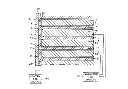
FIG. 1 shows a preferred embodiment of anode
2120699
PCT/l~S 91 /07161
6 ~3 Rec'd P~JT/P~Q 0 l SEP 1993
electrode structure 12 for use in fabricating an
electrophoretic display panel. Electrophoretic display
panels are well known in the art and detailed
descriptions regardi,ng their fabrication and operation
can be found in the U.S. Patents identified above in
the Background of the Invention plus many others.
Thus, for purposes of clarity, the following detailed
description will only show details of the anode
electrode structure of the present invention. Further,
for purposes of illustration, the electrophoretic
display panel which is fabricated using an embodiment
of the inventive anode electrode structure is adapted
to display characters. Lastly, in accordance with the
present invention, a line of displayed characters is
formed utilizing a predetermined number of anode line
segments wherein each anode line segment comprises a
first and a second conductor.
FIG. 1 shows a portion of anode electrode
structure 12 which is fabricated in accordance with the
present invention and which forms at least a portion of
a line of displayed text in the display. Typically,
each anode line is fabricated from a thin layer of IT0
deposited on a glass sheet. The IT0 layers are
practically transparent and fabricated on the glass
sheet by conventional processing techniques as
described in the above-noted patents. The IT0 lines
are deposited on a glass sheet 60. In a typical
electrophoretic display panel which is fabricated in
accordance with the present invention, a line of
displayed text is comprised of 26 anode line segments.
As shown in FIG. 1, anode electrode structure 12 is
comprised of a multiplicity of anode line segments,
however, only segments 2, 7, 13, and 18 are shown for
the sake of clarity. In accordance with the
illustrative embodiment of the present invention, each
SUBSTITIJTE SHEEl~
212~699 ..
PCT/US 91 /o7 l 61
Rec'd P~r/PTO ~ 1 SEP 1993
of anode line segments 2, 7, 13, and 18 is comprised of
two, spaced apart conductors. In particular, anode
line segment 2 is comprised of larger conductor strip
3 and smaller conductor strip 5; anode line segment 7
is comprisPd of a larger conductor strip 8 and smaller
conductor strip 10; anode line segment 13 is comprised
of larger conductor strip 14 and smaller conductor
strip 16; and anode line segment 18 is comprised of
larger conductor strip 19 and smaller conductor strip
10 21.
In a preferred embodiment of the present
- invention, larger conductor strips 3, 8, 14, and 19 are
each .115" wide and smaller conductor strips 5, 10, 16,
and 21 are each .013" wide. Further, the spaces
between the conductors --spaces 4, 6, 9, 11, 15, 17,
20, and 22-- are each .001" wide. As a result of this,
each anode line segment in the preferred embodiment is
.130 " wide.
It should be appreciated that embodiments of
20 the present invention are not limited to an anode
electrode structure having the dimensions given above.
For example, one may fabricate an anode electrode
structure wherein larger conductor strips 3, 8, 14, and
19 are each .110" wide; smaller conductor strips 5, 10,
25 16, and 21 are each .016" wide; and the spaces between
the conductors --spaces 4, 6, 9, 11, 15, 17, 20, and
22-- are each .002" wide. In such an embodiment, each
anode line segment is .130" wide.
It should further be appreciated that
30 embodiments of the present invention are not limited to
an anode electrode structure having uniform dimensions.
As such, an embodiment of the present invention may be
fabricated so that anode line segments associated with
respective lines of displayed text have dimensions
35 first given above as well as anode line segments having
212Qfi99 . - - -
- P~-~SCi/07~
dimensions second given above.
As shown in FIG. 1, smaller conductor strips
5, 10, 16, and 21 are all electrically connected. Such
connections would apply for all anode line segments
5 associated with a g~ven display line of said display
and there would typically be no such connection between
similarly situated conductor strips of different lines.
Of course, it should be appreciated that the present
invention does not require such electrical connection
10 because appropriate voltages, as will be set forth in
detail below, may be applied independently to these
- conductor strips. However, for a panel which is
utilized in a character display mode, the electrical
connection shown in FIG. 1 is preferred. In the
15 preferred embodiment shown in FIG. 1, space 29 between
one end of larger conductor strip 3 and conductor 30 is
.0625" and conductor 30 is .0625" wide.
Table 1 helps illustrate the manner in which
voltages are applied to anode electrode structure 12
20 for use in conjunction with an electrophoretic display
panel to provide full panel erase, "hold", "write", and
selective erase operations in accordance with the
present invention. A full panel erase operation is
provided by applying a negative voltage to all anode
25 line segments 2, 7, 13, and 18, i.e., by applying a
negative voltage to larger conductive strips 3, 8, 14,
and 19 and by applying a negative voltage to smaller
conductor strips 5, 10, 16, and 21. Further, a "hold"
or a "write" operation is provided by applying a
30 positive voltage to all anode line segments 2, 7, 13,
and 18, i.e., by applying a positive voltage to larger
conductive strips 3, 8, 14, and 19 and by applying a
positive voltage to smaller conductor strips 5, 10, 16,
and 21. Lastly, a selective erase operation of a line
35 of text is achieved by applying a negative voltage to
SU~STITUTE SHEET
2l2o699 ,.
PCT/IJS 91 /o7 l 6~
03 Rec'd PCt/PTO O 1 SEP 1993
-
all of the anode line segments associated with that
character line and by applying a positive voltage to
all the anode line segments associated with the other
lines of text.
TABLE I
Operation Voltages for Larger Voltages for Smaller
Conductor Strips Conductor Strips
Full Panel -V -V
Erase
15Hold +V +V
Write +V +V
Selective-V for those +V
20 Erasure of associated with
a line of erased text lines
text to be
+V for those
associated with
other text lines
The respective voltages discussed above are
supplied to the smaller conductor strips as 5, 10, and
so on by a conventional voltage generator 50 and to the
groups of larger conductor strips associated with
corresponding lines of displayed text by an anode line
driver circuit 51. With reference to Table I, however,
it will be observed that the respective groups of
larger conductor strips need not be connected together,
and hence, the larger strips associated with lines of
displayed text above and below a given line of text
being erased can be energized independently of the
those corresponding to the given line. Accordingly,
where anode line segment 7 is the lowermost segment of
a first line of displayed text and anode line segment
SUBSTITUTE SHEET
2120 69~ ..
03 Rec'd P~Y/PTL 8 1 ~EP 1993
13 is the uppermost line segment of the adjacent line
of displayed text beneath the first, one could
selectively erase the line of text by applying a
negative voltage to the large conductor strips as strip
8 associated therewith and a positive voltage to the
smaller conductor strips as 10 associated therewith,
which smaller conductor strips are connected together.
Lines of text which are not to be erased, as the
adjacent one associated with large strip conductor 14
and small strip conductor 16, would be held by applying
a positive voltage to all strip conductors associated
therewith.
Those skilled in the art will recognize that
further embodiments of the present invention may be
made without departing from its teachings and that the
present invention is not limited to the specific
embodiments described above.
SUBSllTUlE SIIE~T