Note: Descriptions are shown in the official language in which they were submitted.
CA 02120792 2004-07-13
i
SEI 94-09
TITLE OF THE INVENTION
Optical Waveguide Device
BACKGROUND OF THE INVENTION
Field of the Invention
The present invention relates to the structure of an
optical waveguide device that functions while a
functional component for performing optical branching,
coupling, switching, and the like is inserted in the path
of an optical waveguide and, more particularly, to a
structure for facilitating manufacture of such a device
which has a small transmission loss in an insertion
region of the functional component.
Related Background Art
An optical device that performs optical branching,
coupling, switching, and the like in a small region on a
millimeter-order is a very important constituent element
for downsizing or increasing the degree of functions of
an optical communication system, an optical sensor, or
the like. As such an optical device, a so-called parts
insertion type optical waveguide device which functions
by inserting a functional component for performing
optical functions such as optical branching, coupling,
switching, and the like in an optical waveguide has been
attracting attention in recent years.
In this optical waveguide device, functions such as
optical branching, coupling, and the like are
1
'94 04/07 20:23 ~C.1' 03 3564 8009 SO);I PAT~TOKYO ->-~-> i~IrIRKS ~J006/060
SET 9409
conventionally realized by fabricating a directional
coupler or an optical waveguide pattern having a
structure of , a . g. , a Y- or X-shaped waveguide, on a
waveguide substrate. The switching function is realized
by varying the propagation constant of the directional
coupler.
Other than the method described above, the functions
of branching, coupling, switching and the like of the
optical waveguide device can be realized by incorporating
9.4 a functional component that performs branching, coupling,
switching, and the like in the path of the optical
waveguide formed on the waveguide substrate.
Fig. 1 shows the arrangement of a conventional
parts-insertion type optical waveguirle device for
realizing the optical branching function. In this
conventional optical waveguide device, a half mirror 2
serving as a functional component for separating light is
inserted at the intersecting portion ~ an insertion region
where the functional component is to be inserted) of a
20 ~-shaped optical waveguide 1. the half mirror 2 has an
angle of 45° with respect to the optical path of the light
to be incident on it. Tn the conventional optical
waveguide device, the GUre width of the optical waveguide
1 is constant (the refractive index difference between
t he core and the cladding layer is also constant) . Tn
this arrangement, light propagating through an incident
2
' 94 04/07 20: 24 ~~ 03 3564 8004 SOEI PAT~TOKYO -~-~~ hIARKS ~J 007/060
n
~1~~~~~
SEI 94-09
side optical waveguide la (the incident side of the half
mirror 2) is separated into a transmission-side optical
waveguide 1b (the exit-side optical waveguide of the half
mirror 2 ) and a reflection-side optical waveguide 1c ( the
reflection-side optical waveguide of the half mirror 2)
by the half mirror 2.
The manufacturing steps of this conventional optical
waveguide device will be described. part of the
intersecting portion (the insertion region where the
functional component is to be inserted) of the T-shaped
optical waveguide 1 formed in advance on the optical
waveguide substrate (a portion indicated by a rectangle
in Fig. 1) is removed with a laser beam or the like to
form a space for inserting the half mirror 2 therein.
Then, the half mirror 2 as the functional component is
inserted.
'The conventional optical waveguide device is
manufactured by perfarming the above manufacturing steps.
SUNMAR71 OF T1HE INVENTION
For example, the manufacturing steps of an optical
waveguide device for optical branching are as follows .
hart of the intersecting portion of the T-shaped optical
waveguide 1 formed in advance on the waveguide substrate
where a functional component, such as a half mirror or a
beam sputter, is to be inserted is removed by a laser
beam process or the like. Then, the functional component
3
'fl4 09/07 20:24 ~ba103 3569 8009 SOEI PAT~TOKYO ->-~-> nIARKS. _ 't~1008/060
sEZ 94-09
for realizing a desired function is inserted in a space
formed by the laser beam process or the like. Generally,
a material forming the optical waveguide and the space
have different refractive indices. Thus, optical
diffraction occurs at this portion, causing an excessive
loss. The excessive loss is a transmission loss caused by
factors other than attenuation of the propagating light.
If the half mirror is not inserted at a correct position,
the traveling path of the light incident on this half
mixror is distorted, leading to an excessive loss again.
Therefore, in order to Correctly insert the
functional Component, the process must be done with a
micron- or submicron-order precision. ~lith an optical
waveguide device according to the present invention, the
countermeasure as described above for decreasing the
excessive loss caused by diffraction and improving a poor
parts-insertion precision is not necessary. Also, this
device can be manufactured easily (without requiring a
high-precision process) with a good reproducibility while
suppressing the transmission loss in the insertion region
as compared to the Conventional device.
The optical waveguide device according to the
present invention is not limited to an optical waveguide
device for optical branching but can also be applied to
other parts-insertion type optical wavegraide devices in
which a functional component for performing optical
4
'94 04/07 20:25 X03 35&4 8004 SOEI PAT~TOKYO -~-~-~ AfARKS 0009/060
SEI 94-09
coupling, switching, and the like is inserted.
An optical waveguide device according to the present
invention comprises a waveguide substrate and an optical
waveguide formed on the waveguide substrate and having a
core for propagating light and a cladding layer covering
the core. The optical waveguide is constituted by one or
at least two optical waveguide regions serving as
transmission paths of an optical signal, an insertion
region having at least one input/output terminal of an
ZO optical signal and in which an optical functional
component for realizing a desired function is to be
inserted, and a first optical connection region having a
first input/output terminal directly connected to one
terminal of the optical waveguide region and a second
input/output terminal directly connected to the
input/output terminal of the insertion region. The mode
field width of light propagating in the insertion; region
is larger than that of light at an arbitrary portion of
the optical waveguide region.
20 In particular, the first optical connection region
has a structure for properly connecting to the optical
waveguide region and the insertion region having
different mode field width of light propagating therein.
zn other words, the first optical connection region has a
structure fox changing the mode f field width of light
which becomes incident from the optical waveguide region
'94 04/07 20:26 X03 3564 8004 SOEI PAT~TOKI'0 -~->-> DIARKS I~j010/060
~~~~'~~2
SET 94-09
side and emerges to the insertion region side or the mode
field width of light which becomes incident from the
insertion region side and emerges to the optical
waveguide region side. Regarding a practical structure,
the core size (e.g. , the core width in the horizontal
direction with respect to the main surface of the
waveguide substrate ) of the core of the first optical
connection region is gradually increased from the first
input/output terminal connected to the optical wavegui~de
1.p region toward the second input/output terminal connected
to the insertion region. The size of the core of the
first connection region is gradually decreased from the
first input/output terminal connected to the optical
waveguide region toward the second input/output terminal
connected to the insertion region. At this time, the core
size is set such that the core size at the f first optical
connection region an the vicinity of the connection
surface with the insertion region becomes smaller than a
core size that minimizes the mode field width of
20 propagating light. In these arrangements, the sectional
shape of the core in the horizontal direction along the
surface of the waveguide substrate is narrowed or widened
at a predetermined taper angle an the traveling direction
of light. In other words, the sectional shape of 'the core
may be similar to a trapezoid.
The optical waveguide of the optical waveguide
6
'94 04/07 20:26 X03 3564 8004 SO1;I PAT~TOKYO -~->-> D1ARKS 0011/060
~'""~
s>~x ~4-09
device according to the present invention may also
comprise a plurality of insertion regions. xn this case,
a second optical connection region is provided between
each pair of insertion regions in order to provide a mode
field width substantially the same as theft of light
propagating in these insertion regions. The second
optical connection region has a core size substantially
the same as that of each pair of insertion regions. The
core size does not change between the incident and exit
sides of light. "'
As described above, in the optical waveguide formed
on the waveguide stabstrate by arbitrarily combining the
optical waveguide region, the first and second optical
connection regions, and the insertion region, a
refractive index difference between the core and the
cladding layer of a region where the first and/or second
. optical connection region directly connected to the
ir~sertian region is disposed is srnaller than the
refractive index difference between the core and the
ZO cladding layer at a predetermined portion of the optical
waveguide region.
Fig. 2 is a graph showing the off-axis dependency of
an optical excessive loss when the optical axis of the
optical waveguide ire the optical waveguide device
according to the present invention is deviated. In
Fig. 2, the broken line indicates the case of an optical
'94 04/07 20:27 ~~03 3564 8004 SOET PAT~TOKYO -~-~-~ hfARKS C~j012/060
SET 94-09
waveguide that sets the mode f field width of prapagating
light to 8 Vim, and the solid line indicates the case of an
optical waveguide that sets the mode field width of
propagating 1 fight to 18 ~.m .
A spot size is a parameter two-dimensionally
expressing the distribution of propagating light at a
predetermined portion of the optical waveguide disposed
Gn the waveguide substrate. In other words, assumzng
that the optical waveguide is cut perpendicularly to t he
traveling direction of light, a spot size means the size
of the distribution of light having a predetermined
light intensity' or more at this section of the optical
saaveguide. More specifically, this distribution can be
two-dimensionally grasped by setting the axis of abscissa
as the distance from the optical axis of the core and the
axis of ordinate as the light intensity.
In this specification, an area of the light
distribution whose light intensity in the horizontal
direction of the waveguide substrate is 1/e2 or more its
peak value is defined as the mode field. The mode field
width is uniformly def fined as the maximum total width in
the horizontal direction of the mode field defined in the
above manner. On the other hand, the spot size, a general
parameter, can be utilized instead of the mode field
width so as to express the characteristics of the present
invention.
8
'94 04/07 20:28 d03 3564 8004 SOEI PAT~TOKI'0 '>1-~ hIARKS ~013/O60
SET 94-a9
As is apparent from Fig. 2, when the mode field width
:is increased, the absolute value of the optical excessive
loss caused by deviation of the optical axis is
decreased. zn other words, the off-axis dependency of
the excessive loss i~ decreased. Therefore, as in the
optical waveguide device according to the present
invention, the path of the optical waveguide for
propagating light has a structure for increasing the mode
field width at the insertion region where an optical
functional component, such as a half mirror or a beam
splatter, is inserted than a mode field width at other
regions. Hence, even if the functional component is
inserted with a poor precision, the excessive loss can be
suppressed as compared to a conventional case wherein the
mode field width is not increased.
The mode field width changes depending on the
wavelength of propagating light, the refractive index
difference between the core and the cladding layer of the
optical waveguide, the core width, the core thickness,
and the like. Therefore, the mode field width at 'the
insertion region where the functional component is to be
inserted can be increased. It might be especially
effective if the core width at the input/output terminal
of the insertion region is set to have a different value
( larger or smaller than the width of the core at other
portions ) from the core width of other regions .
9
'94 04/07 20:28 ~U03 35&4 8004 SOEI PA'1'~TOKYO ->-~-~ MARKS . .014/060
SEI 94-09
For this reason, according to the present invention,
a connection region having a structure in which the core
size {core width) is linearly changed is provided between
the first and second input/output terminals.
Fig. 3 is a graph shaving the relationship between
the core width of the optical waveguide disposed on the
waveguide substrate and the mode field width. The
optical waveguide device of the example shown in Fig. 3 is
manufactured by setting the optical waveguide to an
SiC3a-TiO~ type, the refractive index difference between
the core, serving as the prospective optical waveguide,
and the cladding layer to 0 . 3 0, and the core thickness to
7 ~tm .
d~s is apparent also from Fig. 3, when, of the optical
waveguide, the core width of the optical waveguide region
is,~ e.g. , 7 Vim, the mode field width of this portion
{2nsertion region) is increased by increasing the core
width at the insertion region to be larger than 7 dam ( a
xange indicated by P in Fig. 3). On the other hand, as
shown in Fig. 3, when the core width is decreased to be
smaller than a predetermined value, the mode field width
is increased as well. This is because when the care width
is decreased, the optical power confinement capability of
the core exceeds its limit. ThereFore, in the example of
Fig. 3, when the core width of the optical waveguide
region is 4 Vim, the mode fiend width can be increased by
'94,04/07 20:29 'b'03 3564 8004 SOEI PAT~TOK10 -~->-> DIARKS f~015/060
SEI 94-09
decreasing the core width of the insertion region to
about 2 ~m (the range indicated by Q in Fig. 3) (note that
all the core widths explained above are values at the core
thickness of ? Vim) .
Tn order to increase the mode field width, a means
for decreasing the refractive index difference between
the core and the cladding layer of the optical waveguide
may also be employed. Fig. 4 is a graph showing the
relationship between the refractive index difference
between the core and the cladding layer and the mode field
width. In an optical waveguide device shown in the
example of Fig. 4, the optical waveguide is set to an
Si~Z-fi02 'type, and both the width and 'thickness of the
core serving as the prospective optical waveguide are set
to ? um.
As is apparent from Fig. 4, the mode field width can
be increased by decreasing the refractive index
difference between the core and the cladding layer.
The present invention will become more fully
understood from the detailed description given
hereinbelow and the accompanying drawings which are given
by way o~ illustration only, and thus are not to be
cont~i.dered as limiting the present invention.
Further scope of applicability of the present
invention will become apparent from the detailed
description given hereinafter. However, it should be
11
'9,4109/07 20:29 X03 3564 8004 SOEI PA1'~TOKYO -~-~-> DIARKS X016/060
SEI 94-09
understood that the detailed description and specific
examples, while indicating preferred embodiments of the
invention, are given by way of illustration only, since
various changes and modif ications within the spirit and
scope of the invention will become apparent to those
skilled in the art from this detailed
description.
BRIEF DESCRIPTTON OF THE DRAWINGS
Fig. 2 is a view showing the structure of a
conventional optical waveguide device;
Fig. 2 is a graph showing the relationship between
the deviation of the optical axis, when an optical
functional component is inserted in an insertion region,
and an optical excessive loss in each of two types of
optical waveguides having different mode field widths;
Fig. 3 is a graph showing the relationship between
the core width and the mode field width of an optical
waveguide having a constant core thickness;
Fig. ~ is a graph Showing the relationship between
the refractive index difference between the core and a
cladding layer covering the core, and the mode field
width of light propagating in the optical waveguide;
Fig. 5 is a view showing the arrangement of an
aptical wa,vegui.de device according to err embodiment of
the present invention which realizes an optical branching
function;
12
'94 04/07 20:30 X03 3664 8004 SOEI PAT~TOKYO -~-~-~ hIARKS 0017/060
SE:I 94-09
Fig. 6 is a view for explaining the respective
regions of the optical waveguide device shown in Fig. 5
that constitute the optical waveguide;
Fig. 7 is a view for explaining the respective
regions of an optical waveguide device equivalent to that
shown in Fig. 5 constitutes the optical waveguide;
Fig. 8 is a sectional view of an optical waveguide
region ,~ taken along the line X - X of the optical
waveguide device shown in Fig. 5 and of an optical
waveguide device shown in Fig. 15;
Fig. 9 is a sectional view of the optical waveguide
region A taken along the lines Y - Y and Z - Z of the
optical waveguide devices shown in Figs. 5 and 15;
Fig. 10 is a graph showing the loss frequency
distribution of the optical waveguide device ( 20 samples )
shown in Fig, 5;
Fig. 11 is a graph showing the loss frequency
distribution of the conventional optical waveguide device
(20 samples) shown in Fig. 1;
Fig. 12 is a graph showing the relationship between
the length (taper length) of a connection region C, seen
along the traveling direction of light propagating
through the optical waveguide, and an excessive loss in
the optical waveguide device according to the present
:invention;
Fig. 13 is a view showing 'the structure of an optical
13
'94 04/0? 20:30 n03 3564 8004' SOEI PAT~TOKI'0 ->-~-> hIARKS (~I018/060
SEI 94-09
waveguide type switch as a comparative example of the
optical waveguide device shown in Fig. 15;
Fig. 14 is a view for explaining the respective
regions constituting an optical waveguide in an
application of the optical waveguide device according to
the present invention;
Fig. 15 is a view showing the arrangement og an
optical waveguide type switch as an application of the
optical waveguide device according to the present
20 invention;
Fig. 16 is a view showing the structure of an optical
waveguide type switch as a conventional optical waveguide
device to be compared with the Optical waveguide device
shown in Fig. 15;
Fig. 17 is a graph showing the loss frequency
distribution of the optical waveguide device (20 samples)
shown in Fig. 13;
Fig. 18 is a graph showing the loss frequency
distribution of the optical waveguide device (20 samples)
20 shown in Fig. 15; and
Fig. 19 is a graph showing the loss frequency
distribution of the conventional optical waveguide device
( 20 samples ) shown in Fig . 16 .
:DESCRIPTION OF THE PREFERRED EMBODTMENTS
An optical waveguide device according to the present
invention will be described with reference to Figs. 5 to
14
'94 04/07 20:31 °t3°03 3564 8004 SU);I PA'r~TUKYO a->-~ MARKS .-
1~019/O60
SEI 94-09
19. Note that same portions in the drawings are denoted
by the same reference numerals, and a detailed
description thereof will be omitted.
Fig. 5 shows the arr~azxgement of r~ parts-insarti on
type optical waveguide device having an optical branching
function as a typical embodiment of the optical waveguide
device according to 'the present invention. This optical
waveguide device is constituted by a waveguide substrate
and a T-shaped buried type 5i02-Ti02 optical waveguide 10
formed on the waveguide substrate. A half mirror 2
serving as an optical functional component is inserted at
the intersecting portion (insertion region possibly
adapted to be inserted a functional component) of the
opt~.cal waveguide I0. A dielectric thin film may be used
as the optical functional component.
As shown in Fig. 6, the optical waveguide 10 is
constituted by at least three types of regions A, B, and
The region A is an optical waveguide region having
at least two input/output terminals, the regian A adapted
to b2 a light transmission path .
The region .B is a region having at least one
~.nput/output terminal of propagating light. This region
is an insertion region possibly adapted to be inserted an
optical functional component for realizing a
predetermined function. The mode field width of light
'94 04/07 20:32 ~~03 3564 8004 SOEI PAT~TOKYO -~-~-> B1ARKS C~J0201060
SEI 94-09
propagating in the region B is larger than that of light
at a predetermined portion of the optical waveguide
region .
The region C is a region having a first input/output
terminal directly connected to one input/output terminal
of the optical waveguide region and a second input/output
terminal directly connected to the input/output terminal
of the insertion region . This region C is a first optical
connection region for varying the mode field width of
light propagating in it.
Each of the optical waveguide devices shown in
Figs. 5, 6, and 7 has a structure ~ar changing the mode
yield width of propagating light by continuously changing
the core width of the first connection region C.
In particular, the optical waveguide 10 formed on
the waveguide substrate can be fabricated in accordance
with sputtering, CVD, flame deposition, or the like.
When a quartz-based optical waveguide is to be formed,
flame deposition is effective since it decreases losses.
~0 The manufacturing process of the Si02-Ti02 optical
waveguide 10 in accordance with flame deposition is
disclosed in "Bmall-boss QuartL-Based Optical waveguide"
in Optoronics ( 1992 ) No. 6, Which will be summarized as
follows.
More specifically, fine glass particles obtained by
burning a gas mixture material. of SiCl9 and TiCl~ in
16
'94 04/07 20:32 °Cj'03 3564 8004 SOEI I'AT~TOKI'0 -~-~-~ hIARKS
I7j021/060
SEI 94-09
oxyhydrogen flame are deposited on an Si substrate
(waveguide substrate) 11.. The composition of the fine
glass particles is controlled in this flame deposition
process, thereby forming a two-layered fine particle film
consisting of an Si02 lower cladding layer ( a layer
serving as the prospective cladding layer of the optical
waveguide 10 ) and an Si02-Ti02 core layer ( serving as the
core of the optical waveguide 10 ) .
Subsequently, this two-layered fine particle film
(the Si02 lower cladding layer and the Si02-Ti02 core
layer) is heated to a high temperature of 1,000°C or more
in an electric furnace to form a transparent planar
optical waveguide film. Then, an unnecessary glass film
portion is removed by reactive ion etching, thereby
forming a ridge-shaped core.
Finally, the core is covered with an Si02 upper
cladding layer in accordance with the flame deposition
process again and changed into a transparent glass layer
to foam a cladding layer that constitutes the optical
waveguide 10, thereby manufacturing the optical waveguide
device.
rn the embodiment shown in Fig. 5, of incident-
(incident side of the functional com:ponent),
transmission-, and reflection-side (which are both on the
reflection side of the functional component) optical
waveguides 10a, 10b, and 10c, the width of the core of
17
'9$4/07 20:33 ~CJ03 3564 8004 SOEI PAT~TOK1'0 -~-.-. DIARKS ~022f060
SEI 94-09
each connection region C is increased in the tapered
manner toward the T--shaped insertion region ( insertion
region having three input/output terminals) of the
functional component.
On the other hand, in the embodiment shown in Fig. 7,
of inaident~- (incident side of the functional component),
transmission-, and reflection-side (which are both on the
rarfleatian side of the functional component) optical
waveguides 10a, 10b, and 10c, the width of the core of
each connection region C is decreased in the tapered
manner toward the T-shaped insertion region (insertion
region having three input/output terminals) of the
functional component. A core width w1 at a portion of
the optical waveguide before widened in the tapered
manner, e.g., of the optical waveguide region A is, e.g.,
7 ~.m. More specifically, this corresponds to the core
width of the portion 1.2b indicated by the line X - X in
Fag. 5. Fig. 8 shows 'the sectional view of the portion of
this optical waveguide. A core width W2 at the insertion
region B is, e.g., 20 ~sm. More specifically, this
corresponds to the core width of the portion 12a
indicated by the line Y -- Y in Fig. 5. Fig. 9 shows the
sectional view of the insertion region H. The length of
the first optical connection region C where the care
width is gradually changed with a predetermined taper
angle with respect to 'the optical axis, i . a . , a taper
18
'94/07 20:33 ~U03 3564 8004 SOEI PAT~TOKYO ->-.-> BfARKS X023/060
sz;x 94-09
length L is 2 mm. A thickness T of the core 12a or 12b is
constantly 7 Vim, and the refractive index difference
between the core 12a or 12b and the cladding layer 13 is
0.3~.
The half mirror 2 is inserted in the insertion
~°eg2.on B which is formed to have a T shape in the optical
waveguide 10. The half mirror 2 is mounted at an angle of
.~5'° with respect to the optical axis of the incident light
propagating through the incident-side optical waveguide
10a. The half mirror 2 can be mounted in accordance with
various manners. Generally, a groove for inserting the
half mirror is formed at a corresponding portion of the
insertion region'B of the optical waveguide 10 by an
appropriate means, e.g., a laser beam process, chemical
etching, mechanical cutting, or the like. Thereafter,
the half mirror 2 is inserted in the' formed groove.
In particular, the half mirror 2 of this embodiment
has a thickness of 15 ~,m and vertical and horizontal sides
of 1 mm. This half mirror 2 is designed to transmit 50 0
and to reflect 50~ of light having a wavelength of
1. 31 ~,m .
In the above arrangement, the core v~idth of the care
~.2b in the optical waveguide region A is 7 ~,m and its mode
field width is about 8 Vim. The width of the core 12a at
the input/output terminal of the insertion region B in
the vicinity of the half mirror 2 is 20 ~srn. Accordingly,
19
' 9,4 , 04/07 20: 34 ~f~ 03 3564 8004 SOEI PAT~TOKYO -~->-~ hIARKS ~ 024/060
SEI 94-09
when light having a wavelength of 1.31 ~m becomes
incident on the incident-side optical waveguide 10a, the
mode field of this light is enlarged in the horizontal
direction as this light comes close to the half mirror 2
in the first optical connection region C. When light is
incident on the insertion region B, 50 0 of the incident
light is guided to the transmission-side optical
waveguide 10b and the remaining 500 of the incident light
is guided to the reflection-side optical waveguide lOc by
the half mirror 2.
At this time, a case will be studied wherein the
insertion position of the half mirror 2 in the insertion
region B has a poor precision and thus the optical axes of
the transmission and reflected light are deviated. In
this case, since the mode field width is increased, light
is propagated to the respective optical waveguides 10b
and 10c with a small loss .in the manner described above
with reference to Fig. 2. Figs. 10 and 11 are employed to
confirm this loss decreasing effect.
More specifically, Fig. 10 is a graph of the loss
frequency distribution which evaluates an excessive loss
in the reflection-side optical waveguide 19c obtained
with 20 optical waveguide devices each having the above
ax-rangement. Fig. 11 is a graph of the loss frequency
distribution of the conventional optical waveguide device
having a constant core width of 7 ~m while other
'9.9/07 20:35. ~~03 3564 8004 SOGI PAT~TOKI'0 -~-~-~ nIARKS I~J025/060
sEZ 9~.-09
conditions being set to be the same as those of the above
arrangement.
The excessive loss is supposed to be caused mainly
by the misalignment of the optical axis of the reflected
lights and the center of the core 12a of the
refhecti~n-side optical waveguide 10c du.e to the poor
precision of the insertion position of the half mirror 2
in the manufacturing process. As is apparent from
comparison of Figs. 10 and 11, in the optical waveguide
device according to the present invention, the excessive
loss is smaller than that of the conventional optical
waveguide device, and repeatability of the optical
excessive loss is improved as well. That is, the optical
waveguide device according to the present invention is
less influenced by the poor insertion precision.
In the above embodiment, the mode field width is
increased by increasing the width of the core 12a at a
portion corresponding to one input/output terminal of the
insertion region B, vahere the half mirror 2 is to be
inserted, to be larger than the width of the core 12b of
the optical waveguide region A. As described above,
however, the mode field width can be increased also by
decreasing the core width. 4vhen 'the core width is 7 dam in
the same manner as in the above embodiment, the mode field
width can be increased by decreasing the width of the core
12a at one input/output terminal of the insertion region
21
'9~" 0~ 20:35 X03 3564 8004 SOE1 PAT~TOKYO -~-~-~ bIr~RKS , f~026/060-
S~'I 94-09
B, where the half mirror 2 is to be inserted, to 2 ~m or
less. In this case as well, the excessive loss can be
decreased in the same manner as in the case wherein the
core width is increased (the range Q spawn in Fig. 3).
Even when the core width is constant, the mode field
width can be increased by decreasing the refractive index
difference between the core 12a and the cladding layer 13
at one input/output terminal of the insertion region B to
be smaller than the refractive index difference between
the core 12b and the cladding layer 13 of the optical
waveguide region A (Fig. 4) . To locally decrease the
difference in specific refractive index, the refractive
index of the core 12a at the insertion region B may be
locally decreased. More specifically, in the case of the
above embodiment, the refractive index can be decreased
by diffusing Ti02 in the Si02-Ti02 core 12a into the
surrounding cladding layer 13.
In the above embodiment, the Si02-TiOZ optical
waveguide is shown as the optical waveguide 10. Other
than this, an SiO2-Ge02 opta.cal waveguide can also be used
as a small-loss optical waveguide. when the Si02-Ge02
optical waveguide is used, in order to decrease the
refractive index of the core, GeOz is diffused from a
desired portion in the optical waveguide.
The optical waveguide device in which the half
mirror 2 is inserted in the T-shaped insertion region B of
22
'94 04/07 20:36 n03 3564 8004 SOEI PAT~TOHI'0 -~-~-~ t(ARKS 0027/060
SEI ~~-09
the optical waveguide 10 in order to provide the optical
branching function has been described. ~rhe present
invention is not limited to this specific embodiment but
can also be applied to other optical waveguide devices
that perform optical switching, coupling, and 'the like.
The relationship between the taper length L ( the
length of the connection region B seen along the
traveling direction of light) and the excessive loss o:E a
case wherein the core width of the optical waveguide is
1~ changed in a tapered manner (the core width is gradually
increased or decreased) as 7 ,gym ~ 20 ~,m ~ 7 um is obtained
by calculation. Fig. 12 shows data concerning an optical
wavegu?de in which an optical waveguide region A, a first
optical connection region C, an insertion region B, a
first optical connection region C, and an optical
waveguide region A are connected in series in the above
manner.
As is apparent from Fig. 12, when the taper length is
600 ~m or more, sufficient loss reduction can be
20 achieved.
However, from the above effect, when the first
optical connection regions C ( 800 ~.m in the above
embodiment) having a length ( taper length ) of 600 ~m or
more are directly connected to the four input/output
terminals (the incident and exit sides of the functional
component) of the insertion region B, and four insertion
23
'94 04/07 20:36 ~~03 3564 8004 SOEI PAT~TOKYO -~->-~ JfARKS X028/060
,, - _
SE1 94-09
regions B each having such an arrangement are formed in a
matrix manner as an optical waveguide, an optical
waveguide 'type switch in which mirrors are inserted in
the respective insertion regions B at an angle of 45 ° with
respect to the optical axis of the incident light is
constituted. In the optical waveguide device having this
arrangement, as shown in Fig. 13, two first optical
convention regions ~ and one optical waveguide region A
are present between each pair of the insertion regions B,
1(7 so that the size of the optical waveguide device is
increased accordingly. An optical waveguide type switch
capable of linearly transmitting light or changing the
traveling path of light can be manufactured by mounting
the half mirrors 2, although not shown in Fig. 13, in the
respective insertion regions B to be inclined at an angle
of 45° with respect to the optical axes of light
propagating through the corresponding optical waveguides
~.0, or by removing the mirrors 2.
~'.he present invention can also be applied to an
~0 optical waveguide device in which a filter is inserted irm
the optical waveguide for the purpose of selecting the
wavelength of light. ~Trien a filter is inserted, an
off-axis excessive loss is rarely caused. However, since
an excessive loss caused by the refractive index
difference between the groove, formed fox inserting 'the
Filter, and the optical waveguide can. be decreased by
24
'94 04/07 20:37 d03 3569 8004 SOEI PAT~TOK1'0 -~->-~ hIARKS f~029/060
SEI 94-09
increasing the mode field width, the present invention
can ~e applied to this optical waveguide device.
~,s an application of the optical waveguide device
according to the present invention, an optical waveguide
device for performing above-described optical switching,
coupling, and the like which is constituted by a
plurality of insertion regions B will be described
(Figs. 14 and 15) .
As described above, the optical waveguide according
20 to the present invention is formed by changing the core
width in each region such that the mode field width of
light propagating in each insertion region B becomes
larger than that of light propagating in the
cox°xesponding optical waveguide region A. Accordingly,
for the purpose of preventing an increase in excessive
loss with an abrupt change in core width, the first
optical connection regions C whose core width is
gradually changed from the first to second input/output
terminal are provided between insertion regions H and
20 optical waveguide regions A.
Fig. 14 shows an application of the optical
waveguide device according to the present invention.
3~Tote that the insertion regions ~1 and the first optical
connection regions C may have a structure shown in Fig. 7.
Referring to Fig. 14, each optical waveguide 10 has
an optical waveguide region A having at least two
'94 04/07 20:38 ~~03 3564 8004 SOEI PAT~TOKI'0 -~-~-~ DARKS (7~.t030/060
SEI 94-09
inpwt/output terrninals, the region .~ adapted to be a
light transmission path to provide a predetermined mode
field width to light. Each optical waveguide 10 also has
an insertion region B which is a .region having at least
one input/output terminal of light, the region B possibly
adapted to be inserted an optical functional component
for realizing a predetermined function. fhe mode field
width of light propagating in the insertion region B is
larger than that of light propagating at a predetermined
portion of the optical waveguide region A. Each optical
waveguide 10 also has a first optical connection region C
having a first input/output terminal directly connected
to one input/output terminal of the optical waveguide
region A and a second input/output terminal directly
connected to the input/output terminal of the insertion
region B for changing the mode field width of light
propagating in this region.
Furthermore, this optical waveguide 10 has a second
optical connection region b having a f first input/output
~0 terminal directly connected to the input/output terminal
of one insertion region B and a second input/output
terminal directly connected to the input/output terminal
of the other insertion reg-ion B. The core sizes of the
first and second input/output terminals of the second
optical connection region B are equal to the core sizes of
the input/output terminals of the corresponding insertion
26
' 94 04/07 20: 38 ~~ 03 3564 8004 SOEI PAT~TOKYO -~->-~ 11ARKS l~J 031/060
2
SEI 94-09
regions B to which the second optical connection region D
is connected. Therefore, the mode field width of light
propagating in the insertion regions B is also equal to
that of light propagating in the second optical
connection region D.
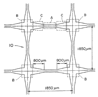
More specifically, as shown in Fig. 15, the core
width of the first optical connection regions C is
increased before propagating light passes through the
plurality of insertion regions B. That is, while the mode
3.~ field width of light once increased is maintained by the
second optical connection regions D, the propagating
light is passed through the plurality of insertion
regions ~. then, the mode field width is returned to the
original size by the first optical connection regions C.
With this arrangement, downsizing of the optical
waveguide device and an increase in integration degree of
the optical functional components are achieved.
In order to confirm the effect of the above optical
waveguide device (Fig. 15) according to the presemt
20 invention, the present inventors made an optical
waveguide device on an experimental basis :invention as
follows.
( 1 ) An optical waveguide type switch as a f first
comparative example, as shown in Fig. 13, which is
fabricated by forming four insertion regions B in a
matrix manner and disposing an optical waveguide region A
27
' 94 04/07 20: 39 n 03 3564 8004 SOEI PA'r~TOKYO ->->-> 11(ARKS f~ 032/060
SEI 94-09
and a first optical connection regions C between each
pair of insertion regions B. In this optical waveguide
device (first comparative example), the refractive index
difference between the core and the cladding layer is
0.3~, and the core width is 7 um. The core width of the
optical waveguide region A is 7 Vim. The core width of the
insertion regions B is 20 Vim. The length of the first
optical connection regions C for changing the core width
from 7 ~,m to 20 ~,m or vice versa, i . a . , the taper length
IO b, is 800 Vim, and the distance between the core centers of
each pair of insertion regions B is 1,850 Vim.
(2) An optical waveguide type switch which is made
as an apglication of the optical waveguide device
according to the present invention, as shown in I;ig. 15.
In this optical waveguide device, the refractive index
difference between the core and the cladding layer is
0.3~, and the core width is 7 um. the four insertion
regions B are formed in a matrix manner. The core width
of each second optical connection region D disposed
20 between each pair of insertion regions I3 is 20 Vim, which
is the same as that of each insertion region B. The
length pf the first optical connection regions C for
changing the core width from ? ~,m to 20 ~.m ar vice versa,
i . a . , the 'taper length Ia, is 800 ~,m, and the distance
between the core centers of each pair of insertion
regions B is 250 ~,m. Note that the sizes of the
28
'94 04/07 20:40 X03 3564 8004 SOEI PAT~TOK1'0 ->->-~ B1ARKS 0033/060
i~v
SEI 94-09
respective portians in Figs . 13 and 15 and corresponding
indicated values are not necessarily disclosed in the
same proportion.
( 3 ) An optical waveguide switch as a second
comparative example which is formed as a conventional
optical waveguide device, as shown in Fig. 16. In this
conventional optical waveguide device (second
comparative example), the refractive index difference
between the core and the cladding layer of the optical
waveguide is 0.3%, and the core width is constantly 7 ~,m.
The distance between the core centers of the intersecting
portions of an optical waveguide 1 is 250 ~.m.
~"wenty optical waveguide device samples that serve
as optical switches for light having a wavelength of
1.31 dam were fabricated for each of three types of optical
waveguide devices, and the excessive loss on the
reflection side was evaluated. Figs. 17 to 19 show the
results.
Fig, 1'~ is a graph showing the excessive loss
frequency distribution of the first comparative example.
Fig. 18 is a graph showing the excessive loss frequency
distribution of the optical waveguide device according to
the present invention. Fig. 19 is a graph showing the
excessive loss frequency distribution of tine second
comparative example (conventional optical waveguide
device shown in Fig. 16 ) .
29
' 94 04107 20: 40 ~ 03 3564 8004 SOEI PAT~'COKYO -~-» DIARKS ~J 034/060
SET 94-09
The excessive loss is supposed to be caused mainly
by the misalignment of the optical axis of the reflected
light and the center of the core of the reflection-side
optical waveguide due to the poor precision of the
insertion position of the half mirror. As is apparent
fxom Figs. 17 to 19, when the optical waveguide device of
the f first comparative example and that according to the
present invention (Fig. 25) were compared with that of
the second comparative example (conventional optical
3.0 waveguide device), it was confirmed that the optical
waveguide 10 having a tapering core at the insertion
region ~ where the mirror 2 (optical functional
component) is to be inserted had a smaller excessive loss
than that of the optical waveguide 1 ( second comparative
example j having a constant core width, and that
repeatability of the excessive loss was improved as well.
When the f first comparative example was compared with
the optical waveguide device according to the present
invention, it was confirmed that 'the latter had a similar
20 small loss although its size was greatly smaller than the
former. In other words, the optical waveguide device
shown in Fig. 1~ can provide the carne effect as that of
the first comparative example while it is capable of
downsizing.
Other examples (applicable embodiments) of the
optical waveguide device shown in Fig. 5 described above
'94 04/07 20:41 ~~03 3564 8004 SOGI PAT°TORI'0 ->->-> MARKS 035/060
SEI 94-09
can be applied to the optical waveguide device shown in
Fig. 1.5.
.As has been described above, according to the
present invention, in order to increase the mode field
width of the insertion region, where a functional
component, e.g., a mirror, is to be inserted, of an
optical waveguide to be larger than the mode f field width
of the optical waveguide region, a connection region i,5
provided in tight contact between the insertion region
and the optical waveguide region, thereby realizing a
desired function. Therefore, a transmission loss caused
by insertion of the functional component can be decreased
as compared to that of the conventional optical waveguide
device.
Furthermore,. according to the application of the
present invention, the same effect as described above can
Sae obtained, and the optical waveguide device can be
further downsized than that of the present invention
described above. These optical waveguide devices can be
2U used as optical devices that are useful in downsizing and
in improving the functions of an optical communication
system, an optical sensar, and the like. As a result, an
optical waveguide device which can be sufficiently
manufactured on a mass production basis without reciuiring
high precision can be provided.
Frorn the invention thus described, it will be
31
'94~f07 20:41 ~ti03 3564 8004 SOEI PAT~TOKI'0 -~->-~ nI:~RKS 1~J036/O60
SEI 94-~09
obvious that the invention may be varied in many ways .
Such variations are not to be regarded as a departure from
the spirit and scope of the invention, and all such
modifications as would be obvious to one skilled in the
art are intended to be included within the scope of the
following claims.
32