Note: Descriptions are shown in the official language in which they were submitted.
-
212~898
LIQUID CRYSTAL APPARATUS
FIELD OF THE INVENTION AND RELATED ART
The present invention relates to a liquid
crystal apparatus, such as a display panel or a
shutter-array printer, using a liquid crystal,
particularly a chiral smectic liquid crystal.
Hitherto, there has been well-known a type of
liquid crystal display devices which comprises a group
of scanning electrodes and a group of signal or data
electrodes arranged in a matrix, and a liquid crystal
compound is filled between the electrode groups to
form a large number of pixels thereby to display
images or information.
These display devices are driven by a multi-
plexing driving method wherein an address signal is
selectively applied sequentially and periodically to
the group of scanning electrodes, and prescribed data
signals are parallelly and selectively applied to the
group of data electrodes in synchronism with the
address signals.
In most of the practical devices of the type
described above, TN (twisted nematic3-type liquid
crystals have been used as described in "Voltage-
Dependent Optical Activity of a Twisted Nematic LiquidCrystal" by M. Schadt and W. Helfrich, Applied Physics
Letters, Vol. 18, No. 4, pp. 127 - lZ8.
2-f2089~
In recent years, the use of a liquid crystal
device showing bistability has been proposed by Clark
and Lagerwall as an improvement to the conventional
liquid crystal devices in U.S. Patent No. 4,367,924;
JP-A (Kokai) 56-107216; etc. As the bistable liquid
crystal, a ferroelectric liquid crystal (hereinafter
sometimes abbreviated as "FLC") showing chiral smectic
C phase (SmC*~ or H phase ~SmH*) is generally used.
The ferroelectric liquid crystal assumes either a
first optically stable state or a second optically
stable state in response to an electric field applied
thereto and retains the resultant state in the absence
of an electric field, thus showing a bistability.
Further, the ferroelectric liquid crystal quickly
responds to a change in electric field, and thus the
ferroelectric liquid crystal device is expected to be
widely used in the field of a high-speed and memory-
type display apparatus, etc.
However, the above-mentioned ferroelectric
2~ liquid crystal device has involved a problem of
flickering at the time of multiplex driving. For
example, European Laid-Open Patent Application (EP-A)
149899 discloses a multiplex driving method comprising
applying a scanning selection signal of an AC voltage
the polarity of which is reversed (or the signal phase
of which is reversed) for each frame to selectively
write a "white" state (in combination with cross nicol
2I20898
polarizers arranged to provide a "bright" state at
this time~ in a frame and then selectively write a
"black" state (in combination with the cross nicol
polarizers arranged to provide a "dark" state at this
time).
In such a driving method, at the time of
selective writing of "black" after a selective writing
of "white", a pixel selectively written in "white" in
the previous frame is placed in a half-selection
state, whereby the pixel is supplied with a voltage
which is smaller than the writing voltage but is still
effective. As a result, at the time of selective
writing of "black" in the multiplex driving method,
selected pixels for writing "white" constituting the
background of a black image are wholly supplied with a
half-selection voltage in a 1/2 frame cycle (1/2 of a
reciprocal of one frame or picture scanning period~ so
that the optical characteristic of the white selection
pixels varies in each 1/2 frame period. As a number
of white selection pixels is much larger than the
number of black selection pixels in a display of a
black image, e.g., character, on a white background,
the white background causes flickering. Occurrence of
a similar flickering is observable also on a display
of white characters on the black background opposite
to the above case. In case where an ordinary frame
frequency is 30 Hz, the above half-selection voltage
2120898
is applied at a frequency of 15 Hz which is a 1/2
frame frequency, so that it is sensed by an observer
as a flickering to remarkably degrade the display
quality.
Particularly, in driving o~ a ferroelectric
liquid crystal at a low temperature, it is necessary
to use a longer driving pulse (scanning selection
period~ than that used at a 1/2 frame frequency of 15
Hz for a higher temperature to necessitate scanning
drive at a lower 1/2 frame frequency of, e.g., 5 - lO
Hz. This leads to occurrence of a noticeable
flickering due to a low frame frequency drive at a low
temperature.
In order to prevent the ~lickering, there has
been proposed a "multi-interlaced" scanning drive
scheme, wherein the scanning lines are selected a
prescribed plurality of lines apart in one vertical
scanning (U.S. Patent No. 5,233,447).
In case where the above-mentioned drive
scheme is applied to display of a background pattern,
a hatching, etc., as usually displayed on a computer
display terminal or a work station display,
particularly noticeable flicker can be observed in
some cases. According to our study, it has been
discovered that the flicker is attributable to the
fact that the above-mentioned images, such as a
background pattern and a hatching displayed on the
21211898
computer display terminal or workstation display,
include a periodically repetitive pattern appearing at
every 2nd, 4th, 8th, ... 2m-th pixel or line ~m = an
integer), and the period of the periodical display
pattern can sometimes be synchronized with the
frequency or period of selection of the scanning lines
in the interlaced scanning scheme to cause a
noticeable flicker.
SUMMARY OF THE INVENTION
A principal object of the present invention
is to provide a liquid crystal apparatus capable of
displaying good images with less synchronization of
the image pattern-repeating period and the periodical
selection of drive lines in a multi-interlaced
scanning scheme, thus providing good images with less
flickering.
According to the present invention, there is
provided a liquid crystal apparatus, comprising:
a liquid crystal device comprising a pair of
substrates respectively having thereon a plurality of
scanning lines and a plurality of data lines
intersecting the scanning lines, and a liquid crystal
disposed between the substrates so as to form a matrix
of pixels each at an intersection of the scanning
lines and the data lines, and
drive means adapted for driving the liquid
212089~
crystal device under conditions that (1) the scanning
lines are sequentially selected so that every N-th
scanning line is selected in a field, (2) N is an odd
number, (3) a period for selecting each scanning line
is changed depending on an environmental temperature
at which the device is placed, and (4) N is changed
depending on the environmental temperature.
These and other objects, features and
advantages of the present invention will become more
apparent upon a consideration of the following
description of the preferred embodiments of the
present invention taken in conjunction with the
accompanying drawings.
BRIEF DESCRIPTION OF T~E DRAWINGS
Figure lA shows an example of time-serial
drive signal waveforms used in the present invention,
and Figure lB shows two types of data signals involved
therein.
Figure 2 is a block diagram of an embodiment
of the liquid crystal display apparatus according to
the present invention including a graphic controller.
Figures 3A - 3D show display pattern examples
for evaluating the occurrence or absence of flic~er.
Figure 4A shows a display pattern and Figure
4B shows a set of scanning signals, data signals and
pixel voltages applied at the time of non-selection
-
-7~
for displaying the pattern shown in Figure 4A.
Figure 5 is a graph showing temperature-
dependent optim~m drive conditions in Example 1.
DESCRIPTION OF THE P~EFERRED EMBODIMENTS
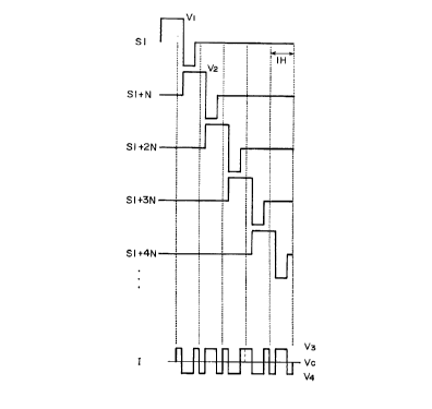
Figure lA shows an example of a partial set
of time-serial drive signal waveforms and Figure lB
shows two types of data signals used in an embodiment
of the drive scheme adopted in the liquid crystal
display apparatus according to the present invention.
Referring to Figure lA, at Sl, Sl+N,
Sl+2N, ... are respectively shown scanning selection
signals applied to a first scanning line, a (l+N)-th
scanning line, a (1+2N}-th scanning line, ... (N:
natural number satisfying N ~ 33, and these scanning
lines are scanned in this order. In this drive
scheme, however, not all the scanning lines are
selected in this order but the scanning lines are
selected with N-l lines apart, i.e., every N-th
scanning line is selected, in one vertical scanning.
In Figure lA, at I is shown a succession of voltage
signals applied to a data ~signal3 electrode I,
including a unit data signal I(B) for displaying a
bright state and a unit data signal I(D) for
displaying a dark state, which have mutually inverted
polarities, as shown in Figure lB. A pixel state is
determined by selecting either one of the data signals
.~
' ~ -
-8~ 8 9 ~
I(~) and I(D).
Next, a relationship between the occurrence
of a flicker and the above-mentioned number N in an
interlaced scanning scheme when the drive signals
shown in Figures lA and lB are used. Now, a drive
operation for displaying one whole picture is referred
to as one frame. In a multi-interlaced scanning
scheme, one frame is divided into N times of vertical
scanning operation, i.e., N fields, in each of which
every N-th scanning line is selected sequentially.
The flicker caused by synchronization of the signal
waveform and the frequency of scanning during the
multi-interlaced scanning scheme is related with the
frequency of a certain display state in a field.
Herein, a field frequency F is defined as: F = Nxf,
wherein f denotes a frame frequency.
The flicker in a scanning-type display device
is caused by a periodical brightness change occurring
during repetitive scanning for forming a picture. In
order to suppress the flicker, it is generally
practiced to shorten the period (i.e., increase the
frequency) of such a periodical brightness change,
thereby making the brightness change unnoticeable to
human eyes.
Also in a ferroelectric liquid crystal
display device, the field frequency F may be increased
by (13 increasiny the frame frequency f or (2)
B
2~-20~9~
increasing the number N in order to increase the
frequency of the brightness change.
The measure (1) of increasing the frame
frequency is accompanied with a problem that, in the
case of a large liquid crystal panel having a large
information capacity (having a large number of
scanning lines), a selection time allotted to one
scanning line becomes short, so that the signal
waveform applied to a liquid crystal layer as a
capacitive load is liable to be distorted, thus
failing to provide a satisfactory image quality.
Further, in the case of using a ferroelectric liquid
crystal driven in response to a pulse, the pulse width
becomes short, thus requiring a high drive voltage and
therefore a high withstand voltage drive, so that the
designing of the driver and also a countermeasure for
dealing with heat evolution from the panel become
difficult. Accordingly, there is practically a limit
in increasing the frame frequency, particularly for a
large capacity display.
The measure (~) of increasing the number N is
effective for preventing the flicker even in case of
not effecting the interlaced selection scanning but,
on the other hand, a larger N is accompanied with an
increased liability of causing an image disorder at
the time of image rewiring, so that a smaller value of
N is desired in this respect.
o~ ~ ~
-10-
In order to obtain an adequately set value of
N, a series of experiments were performed by using a
set of drive waveforms as shown in Figures lA and lB
with different values of N and a liquid crystal
display apparatus asshown in Figure 2. More
specifically, the liquid crystal display apparatus
shown in Figure 2 comprised a display panel 1 having
1024x1280 pixels to whlch scanning signals were
supplied from a scanning line driver 2 and data
signals were supplied from a data line driver 3; a
graphic controller 4 including a display panel
controller 41 for controlling the scanning line driver
2 and the data line driver 3 and a drive power supply
42 for supplying levels of voltages to the drivers 2
and 3, and also an image data supply 5 including a
data generating unit 51 and an image memory 52 and
supplying image data to the display controller 4. The
liquid crystal used in the liquid crystal panel 1 was
pyrimidine-based mixture ferroelectric liquid crystal
having a spontaneous polarization Ps = 5 nC/cm~ and an
apparent tilt angle ~ = 18 degrees. Referring to
Figure lA, the drive voltages V1 - V4 had levels of V
= -V2 = 16 volts and V3 = -V4 = 4 volts with respect
to a central voltage Vc of an AC supply. The drive
conditions for obtaining good images were found to be
as follows at 30 ~C and 45 ~C, respectively:
At 30 ~C
B
0 8 ~ ~
One-line selection period (lH) = 95 ~sec
Frame frequency = lO Hz
At 45 ~C
One-line selection period (lH) = 70 ~sec
Frame frequency = 14 Hz
Under the above-mentioned drive conditions,
several image patterns shown in Figures 3A - 3D were
displayed to ~A~; ne whether a flicker occurred or
not. Figure 3A shows a wholly white pattern. Figure
3B shows a wholly black pattern. Figure 3C shows a
central white rectangular pattern surrounded by a
rectangular black frame. Figure 3D shows a central
pattern of white and black lines alternating every
other line and a rectangular black frame.
The results of the above test are shown
below.
~ .
2120898
(1) Case of frame frequency (f) = 10 Hz
Every N-th
line scan (N) 1 2 3 4 5 6 7 8
Field
frequency (F) 10 20 30 40 50 60 70 80
[Display pattern]
Fig. 3A x o o o o o o o
Fig. 3B x o o o o o o o
Fig. 3C x x x o o o o o
Fig. 3D x x x x o x o x
(2) Case of frame frequency (f) = 14 Hz
Every N-th
line scan (N) 1 2 3 4 5 6 7 8
Field
frequency (F) 10 20 30 40 50 60 70 80
[Display pattern]
Fig. 3A x o o o o o o o
Fig. 3B x o o o o o o o
Fig. 3C x o x o o o o o
Fig. 3D x o x x o x o x
-13-
In the above tables, o represents the
suppression of a flicker to a practically satisfactory
level, and x represents the occurrence of noticeable
flicker.
As is understood from the above results, the
occurrence of flicker was affected by the displayed
image pattern. This is presumably due to the
following two factors:
(13 A difference in optical response between a
selected line and a nonselected line is periodically
recognized.
(2) In displaying an image pattern including
black and white states in mixture, a signal applied at
the time of non-selection is periodically distorted
due to an effect of drive waveform transmission delay
caused by a wiring resistance within a liquid crystal
panel, thereby resulting in a periodical difference in
optical response.
From the experimental results, it has been
found that an image pattern including black and white
display states in mixture requires a higher field
frequency in order to alleviate the flicker compared
with the case of displaying a wholly white or wholly
black pattern. The occurrence of flicker caused by
the factor (2) is described with reference to Figures
4A and 4B.
Figure 4A is a reproduction of the pattern
B
-l4-
212~898
shown in Figure 3C together with indication of some
data electrodes Ia and Ib and periods tl - t3 of
scanning relevant for describing the display of the
pattern. Figure 4B shows a set of drive signal
waveforms applied to display the pattern shown in
Figure 4A. In this case, the scanning is performed
sequentially downwards, i.e., from the top to the
bottom. In the display pattern, all the pixels on a
data line Ia are placed in a dark state, and the
pixels on a data line Ib are placed in either a dark
state or a bright state. Corresponding data signals
are applied to these data lines. As shown in Figure
4B, both the lines Ia and Ib are supplied with a dark
signal in a period tl. In a period t2, the line Ia is
supplied with a dark signal while the line Ib is
supplied with a bright signal. As has been described
before, the dark and bright data signals are
substantially identical in shape but reverse in
phases.
At the time when these data signals are
applied, voltages as shown at S in Figure 4B are
induced on scanning lines. Particularly, in the
periods tl and t3, all the data signals are
rectangular waves of identical phases, voltage rises
(ripples) are induced as shown at Figure 4B ~ at the
time of polarity inversion of the rectangular voltage
waveforms of the data signals. On the other hand, in
~120~
the period t2, the data signal voltages are
rectangular waveforms of mutually opposite phases, so
that the induced ripples are cancelled with each
other, whereby no ripples are caused as shown at
Figure 4B ~ .
Voltage waveforms applied to the pixels at
the time of non-selection as combinations of the
above-described scanning signals and data signals are
shown at Ia - S and Ib - S in Figure 4B. In the
periods tl and t3, the voltage waveforms are
substantially weakened by the induced ripples. In the
period t2, the waveform delay is little. In this way,
during the non-selection period, the voltage waveform
at the time of tl or t3 and the voltage waveform at
the time of tZ are alternately, i.e., periodically,
repeated to cause a periodical difference in
electrooptical response of the liquid crystal, whereby
a flicker is caused.
Incidentally, in the case of displaying an
image pattern as shown in Figure 3C (or Figure 4A),
the cycle of the above-mentioned change in
electrooptical response of the liquid crystal at the
time of non-selection causing a flicker coincides with
the field frequency. Generally, no flicker is
recognized at a frequency of 40 ~z or higher so that,
in the case of a frame frequency is 10 Hz,
substantially no flicker is observed if N is set to 4.
-16-
212~89~
Next, it is assumed that an image pattern as
shown in Figure 3~ (wherein a central region
surrounded by a frame in the black state is composed
of every other white and black lines) is displayed by
a drive under a frame frequency f = 10 Hz and N = 4.
In the case of N = 4 (that is, every 4th
scanning line is selected sequentially~, one picture
is formed by 4 fields and the bright state is
displayed by scanning line in 2 fields among the four
fields.
For example, if the central part of the
pattern shown in Figure 4A includes several pairs of a
bright line and a dark line, so that the dark lines
are placed on even-numbered lines and the following
lines are scanned in the respective fields:
~st field ... (4n+0)th lines,
2nd field ... (4n+1~th lines,
3rd field ... ~4n+2)th lines, and
4th field ... (4n+3)th lines,
the bright state lines are scanned in the first and
third fields. As a result, the waveform ~ is
included in the first and third fields and the
frequency of optical response change is reduced from
40 Hz to 20 Hz, i.e., a half, whereby a flicker is
recognized. Even if the order of fields is exchanged,
the synchronization of the image pattern and the
selected scanning line is still caused, thus resulting
2120898
in a flicker.
In order to effectively suppress the
occurrence of a flicker in the case of displaying a
pattern including a repetition at every 2m-th line (m
= natural number) frequently encountered according to
a multi-interlaced scanning scheme of selecting every
N-th scanning line in one vertical scanning, it has
been found preferable to adopt the conditions of:
(l) a field frequency F > 40 Hz,
(2) N is an odd number.
In the present invention, it is preferred to
additionally change one-line selection period lH
depending on a change in environmental temperature so
as to compensate for a change in response of the
liquid crystal to an applied electric field, thereby
giving a better quality of images.
Herein, some specific embodiments of the
present invention will be described.
(Example l)
The above-described liquid crystal panel was
driven by using a set of drive signal waveforms shown
in Figures lA under the conditions of the scanning
selection pulse voltage heights Vl = -V2 = 16 volts
and a rectangular data signal waveform peak heights V3
= -V4 = 4 volts while optimizing the frame frequency f
and the one-line selection period lH depending on the
temperature according to relationships shown in Figure
212089~
5. Further, the number of interlacing or number of
fields (N) was changed corresponding to the
temperature as follows:
Temp. (~C)
>42 3
25 - 4Z 5
15 - 25 7
5 - 15 9
As a result, good image quality was attained
over the whole temperature ranges.
During the interlaced scanning operations,
the scanning lines were selected in the following
orders.
In the case of N (number of fields) = 3,
(3n+0)th scanning line -~ 13n+l)th scanning line -~
(3n+2)th scanning line (n: integer).
In the case of N = 5, (5n+0)th line
(5n+3~th line . (5n+2)th line - (5n+4)th line -~
(5n+1~th line.
In the case of N = 7, (7n+0~th line -~
(7n+3)th line - (7n+2~th line -~ (7n+5)th line
(7n+63th line -~ (7n+1)th line - (7n+4)th line.
In the case of N = 9, (9n+0)th line
(9n+3)th line -~(9n+6)th line ~ (9n+1)th line -~
(9n+4)th line ~ ~9n+7)th line - (9n+2)th line _
(9n+5)th line -~ (9n+8)th line.
In the cases of N = 5 to 9, the order of
-19-
2120898
field selection was performed at random (i e., so that
adjacent scanning lines are not selected within a
period of at least two consecutive fields3 so as to
avoid the deterioration of image quality due to an
upward or downward image flow encountered in the case
of orderly field scanning.
(Example 2)
The drive operation of Example 1 was repeated
except that the number of fields (N3 was changed in
1~ two ways depending on the temperature as follows:
Temp. t~C3 N
2 25 5
5 - 25 7
The order of field selection was performed at random
in the same manner as in Example 1.
Also in this case, good image quality was
accomplished over the entire temperature regions. By
reducing the variation of N corresponding to the
temperature change, the control system could be
simplified than in Example 1.