Note: Descriptions are shown in the official language in which they were submitted.
_1_
Descri tion
Microprocessor-Controlled Strobe Liqht
Background of the Invention
This invention relates to circuits for electronic
strobe lights utilizing microcontrollers and micro-
processors. Strobe lights are used to provide visual
warning of potential hazards or to draw attention to an
event or activity. An important field of use for
strobe lights is in electronic fire alarm/systems,
frequently in association with audible warning devices
such as horns, to provide an additional means for
alerting those persons who may be in danger. Strobe
alarm circuits include a flashtube and a trigger
circuit for initiating firing of the flashtube, with
energy for the flash typically supplied from a
capacitor connected in shunt with the flashtube. In
some known systems, the flash occurs when the voltage
across the flash unit (i.e., the flashtube and
associated trigger circuit) exceeds the threshold value
required to actuate the trigger circuit, and in others
the flash is triggered by a timing circuit. After the
flashtube is triggered it becomes conductive and
rapidly drains the stored energy from the shunt
capacitor until the voltage across the flashtube has
decreased to a value at which the flashtube
extinguishes and becomes non-conductive. In a more
specific sense, the present invention relates to
apparatus for charging the energy-storing capacitor in
a more precise and efficient manner.
Underwriters Laboratories provides certain
specifications that must be met by the alarms for life
safety use. For example, the flash rate of the strobe
2~.2~~
_2_
must meet a minimum requirement for the range of
voltages for which the flash alarm is to operate.
Supply voltage to strobe alarms, even though
typically D.C., often varies in a range of 20 to 31
volts. Changes in voltage due to various conditions
such as brown outs can vary the supply voltage applied
to the strobe alarm during operation by~as much as 4 to
5 volts. In order to ensure that the minimum energy
requirements were met, strobe alarms were designed to
expend the required energy for the lowest reasonably
expected supply voltage. As a consequence, supply
voltages greater than the lowest reasonably expected
value would (1) unnecessarily expend energy in the
flash above the minimum, (2) more often than needed
and/or (3) in a manner that was not useful.
Far example, the capacitor across the flashtube
charges faster in the presence of a higher input
voltage. If the flash is actuated sensing the
potential across the capacitor, the frequency of the
flashes increases in response to the increased input
voltage. In addition to wasting energy, the increased
frequency also causes unnecessary.wear and tear on the
capacitor and the flashtube. In another example, where
the flash is actuated from a separate timing circuit, a
higher input voltage will cause overcharging of the
capacitor, or at least make it necessary to provide a
larger capacitor than should be necessary. As a
result, the potential across the capacitor will cause a
larger than necessary flash, thereby wasting energy.
Whether it is the flash frequency or the flash
intensity that is increased, energy is being wasted.
This is of special concern when the voltage source is a
battery supply. Wasted energy translates into a
shorter battery life span. Thus, being able to provide
precisely sufficient energy per flash at a constant
frequency will permit meeting minimum standards of
~d
_3_
energy output while at the same time minimizing
unnecessary expenditure of energy, number of flashes
and wear and tear on all components, thus extending the
life of the components.
Another problem associated with prior art strobe
alarms is. the surge in current caused by cycling the
switch used to control the storing of the energy for
the flash. By storing energy .in a small duty cycle
(i.e., in one flash cycle, storing energy for a number
of short periods of time interspersed with longer
periods of inactivity), higher peak currents are
required than if longer charging periods with shorter
inactive times were used: The commonly used short duty
cycles increase the chances of a current overload
resulting in.the tripping of a circuit breaker or
blowing of a fuse, especially when power from one
source is supplying more than one alarm, or other
devices, such as a control panel. Moreover, current
surges, often maximized upon commencing charging
immediately after a flash, create problems in practical
applications.
In order to overcome the above-described disadvan-
tages and shortcomings of known prior art circuits, an
object of the present invention is to provide an
improved strobe light circuit wherein the energy
expended by the flash has decreased fluctuation, is
less dependent on the supply voltage, if at all, and
does not vary substantially the flash rate or the flash
intensity.
Another object of the invention is to provide a
strobe light circuit which provides with few components
a constant~flash rate and intensity.
A further object is to provide a strobe light
circuit which has a higher operating efficiency than
prior art circuits by avoiding unnecessary energy
_q_
losses through precision charging of the energy storage
element in shunt with the flashtube.
A further object is to provide a strobe light
circuit utilizing lower peak charging currents in order
to minimize surges and possible tripping of circuit
breakers or blowing of fuses.
A still further object is to provide a strobe
light circuit that can be driven by either a D.C.
voltage input or a full wave rectified voltage input.
Summary Of The Invention
The strobe light circuit in accordance with the
invention is powered by an input voltage that may vary.
The circuit is used to flash a flashtube at a predeter-
mined flash rate with a predetermined amount of energy
in each flash, notwithstanding the variation of the
input voltage. The circuit includes a first energy
storage device, such as an inductor, supplied from the
input voltage. Also,. there is a second energy storage
device, such as a capacitor, connected in shunt with
the flashtube. This second device for storing energy
is capable of storing energy at a rate faster than the
first energy storage device. A switch, such as a
transistor, regulates the storage over time of energy
in the first energy storage device and allows the
transfer of energy from the first energy storage devicd
to the second energy storage device. The switch has a
first position and a second position such that when the
switch is in the first position, energy is stored in
the first energy storage device and when the switch is
in the second position, energy from the first energy
storage device is transferred to the second energy
storage device. A relative peak current drawn by the
first energy storage device is attained just as the
switch changes from its first position to its second
position.
S ~ ~7 '~ t'1, e'!
i. ~,~ ~. ~ ,:,~ ~J
_5_
A device such as a diode permits current flow from
the first energy storage device to the second energy
storage device and blocks current flow from the second
energy storage device to either the first energy
storage device or the switch. A triggering circuit is
used to flash the flashtube at the predetermined flash
rate.
A microcontroller, powered by a regulated voltage
supply, initiates the triggering circuit at the pre-
determined flash rate. A regulator is used to convert
the input voltage into the regulated voltage supply.
The microcontroller also receives the input voltage and
then samples and digitizes it into a lookup table input
having a corresponding D.C. lookup table output. The
lookup table is either software or part of the firmware
of the microcontroller. The microcontroller repeatedly
cycles the switch between flashes of the flashtube by
controlling the time the switch is in its first
position. The lookup table output provides the signal
for determining the time the switch remains in its
first position. The time interval from the last flash
of the flashtube controls the time the switch is in its
second position.
Overall, the cycling of the switch is controlled
such that the second energy storage device acquires the
predetermined amount of energy for the flash of the
flashtube just as the triggering circuit is initiated
by the microcontroller. Moreover, the microcontroller
controls the switch in a way such that the time the
switch is in its first position is maximized and the
time the switch is in its second position is generally
decreased relative to the time since the last flash of
the flashtube. This helps to minimize the peak current
drawn by the first energy storage device.
In addition, the strobe light circuit according to
the invention is capable of determining if the input
~~ ~~.~..~a;'eD
-6-
voltage is D.C. or is full wave rectified. The micro-
controller after digitizing the input voltage uses a
second lookup table, in this case an internal full wave
rectified lookup table, for providing a different
output corresponding to the lookup table input when the
input voltage is determined to be full wave rectified.
Thus, the~time the switch is in its first position is
controlled by the full wave rectified lookup output
instead of the D.C. lookup table output. The
microcontroller varies the full wave rectified lookup
table output only if the input voltage sampled and
digitized is greater than the previous input voltage
sampled and digitized. The microcontroller samples and
digitizes the input voltage at a frequency equal to the
frequency in which the switch cycles, utilizing the
previous full wave rectified lookup table output to
control the switch until the next input voltage is
sampled and digitized.
Other objects, features and advantages of the
invention will become apparent, and its construction
and operation better understood, from the following
detailed description of the currently preferred
embodiment, read in conjunction with the accompanying
drawings.
Brief Description Of The Drawin~~s
Fig. 1 is a circuit diagram showing in detail a
preferred embodiment of the strobe circuit according to
the invention;
Fig. 2 is a block diagram of the circuit shown in
Fig. 1;
Fig. 3(a) is a flow chart of the functions of the
microcontroller in the first preferred embodiment;
Fig. 3(b) is a flow chart of the interrupt
function of the microcontroller in the first preferred
embodiment;
-7-
Fig. 4(a) is an illustration of the average peak
current of a prior art circuit (low voltage);
Fig. 4(b) is an illustration of the average peak
current of a prior art citcuit (high voltage);
Fig. 4(c) is an illustration of the average peak
current of the preferred embodiment (low voltage);
Fig.4(d) is an illustration of the average peak
current of the preferred embodiment (high voltage);
Fig.4(e) is an illustration of the average peak
current of the preferred embodiment showing a change in
OFF time;
Fig. 5(a) is a flow chart of the functions of the
microcontroller capable of being driven by full wave
rectified input; and
Fig. 5(b) is a flow chart of the interrupt
function of the microcontroller capable of being driven
by full wave rectified input.
Detailed Description Of The Preferred Embodiment
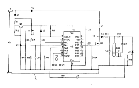
Referring to the electric circuit diagram of Fig.
1 and the block diagram of Fig. 2, a first embodiment
of the invention is connected across a D.C. voltage
source 20, not shown in Fig. 1, which supplies a
voltage Vm. The supply voltage Vm may have a wide range
of values, from 20 volts to 31 volts, for example. The
voltage is applied through a diode D1, which typically
has a voltage drop of 0.7 volt, to a regulator 22 which
includes resistors R1, R2, R3 and R4, switch Q1 and
integrated circuit U1 in order to provide regulated
5.00 ~ 1% volt supply to the V~ input of micro-
controller U2. A precise V~~ input voltage is vital for
the analog to digital reference input of microcon-
troller U2. Resistor R1 is connected at one end to
diode D1 and at the other end to both resistor R2 and
the collector of switch Q1, which in this instance is a
transistor. The other end of resistor R2 is connected
'~ ~~ ~ t~
..~ CJ ..t
. 8 .
to the base of switch Q1 and integrated circuit U1,
which acts as a controlled Zener for providing a
precise 5.00 ~ 1% voltage supply. Resistor R3 is
connected between the emitter of switch Q1 and the
control pin of integrated circuit U1. Resistor R4 is
connected. at one end to both resistor R3 and the
control pin of integrated circuit U1 and at the other
end to one end of integrated circuit U1, which is at
the negative node l0 of the voltage source. Resistors
R3 and R4 are of equal value for biasing integrated
circuit U1.
A reset circuit 24 includes diode D2, resistor R5
and capacitor C1. Diode D2 and resistor R5 are
connected to each other in parallel, and at one end to
the emitter of switch Q1 and at the other end to both
capacitor C5 and the clear input to microcontroller U2.
The other end of capacitor C5 is connected to the
negative node l0 of the voltage source.
As stated above, microcontroller U2 is supplied
with a regulated 5 volt supply at V~~. V~ is connected
to the negative node 10. Capacitor C2 is connected
across V~~ and V~ and acts as a filter. Resistor R6,
acting as a shield, is connected between an input of
microcontroller U2 and negative node 10.
The resonator circuit 26 consists of oscillator
Y1, capacitor C3 and capacitor C4. Oscillator Y1
provides 4 l~iz oscillation to the microcontroller U2
and is connected across the two oscillator inputs of
the microcontroller U2. Capacitor C3 is connected
between the first oscillator input and the negative
node 10. Capacitor C4 is connected between the second
oscillator input and the negative node l0.
An analog to digital input feed network 28 is used
to provide microcontroller U2 with a voltage level
proportional to Vm. The network includes resistor R7,
resistor R8, potentiometer P1 and capacitor C5.
_g_
Resistors R7 and R8 and potentiometer P1 form a voltage
divider. Potentiometer P1, used for fine tuning the.
voltage divider, is connected at one end at the common
node between diode D1 and resistor R1. The other end
of potentiometer P1 is connected to resistor R7, which
in turn is connected to resistor R8 and the analog to
digital input of microcontroller U2. The other end of
resistor R8 is connected to negative node 10.
Capacitor C5 is connected in parallel across resistor
R8 and functions as a filter.
Prior to describing in detail the function of
microcontroller U2, the components affected by micro-
controller U2 will be described. Across Vm is a branch
with diode D3, inductor L1 and switch Q2. Diode D3 is
connected between Vm and inductor L1 and has approxi-
mately a 0.7 voltage drop across it. Inductor L1 is a
first energy storage device 30 for transfer of energy
to the triggering circuit. Inductor L1 is connected
between~diode D3 and switch Q2. The other end of
switch Q2 is connected to negative node 10. Switch Q2
in this embodiment is a MOSFET transistor which cycles
between a conducting state (i.e., position) and a
nonconducting state and is controlled by an output of
microcontroller U2. A voltage divider including
resistor R9 and resistor R10 connects the output of
microcontroller U2 to the gate of switch Q2. One end
of resistor R9 is connected to the output of
microcontroller U2 and one end of resistor R10 is
connected to negative node 10. When switch Q2 is
closed, node 12, between inductor Ll and switch Q2, is
pulled to the same potential of negative node 10. In
other words, inductor L1 is across Vm and the flashing
circuit through diode D4 is isolated. With switch Q2
closed, inductor L1 stores energy until it reaches its
steady state level or until switch Q2 is opened. When
switch Q2 is opened, the energy stored in inductor L1
-10-
is at least partially transferred through diode D4 and
resistor Ril to.charging capacitor C6, the second
energy storage device 32. By controlling the opening
and closing of switch Q2, the rate of storing energy in
inductor L1 is regulated, thereby regulating the
storage of energy across charging capacitor C6.
The flashing circuit 34 includes diode D4,
resistor R11, charging capacitor C6 and flashtube DS1.
Charging capacitor C6 and flashtube DS1 are connected
in parallel, one end of the two components being
connected to negative node 10. Diode D4 and resistor
R11 are connected in series, one end of diode D4 being
connected between inductor L1 and switch Q2. Diode D4
permits current flow into the flashing circuit but
prevents discharge of charging capacitor C6 when the
potential across it is higher than Vm or the potential
across inductor L1. One end of R11 is connected to the
other end of the parallel combination of charging
capacitor C6 and flashtube DS1.
The triggering circuit 36 includes triggering
transformer T1, resistor R12, capacitor C7, SCR Q3,
resistor R13, capacitor C8 and resistor R14. Output
PA2 of microcontroller U2, at the appropriate time,
signals SCR Q3, triggering transformer T1 to pulse
flashtube DS1. Resistor R14 provides over voltage and
current protection to output PA2. Capacitor C8 and
resistor R13 ensure that only the leading edge of the
PA2 pulse reaches the gate of SCR Q3, which only
requires a small pulse. Resistor R13 helps isolate SCR
Q3 from noise. The potential across capacitor C7
slowly reaches the potential across charging capacitor
C6. The rate of potential increase across C7 is
dictated by resistor R12. When SCR Q3 is fired,
capacitor C3 is in effect across the primary of trigger
transformer T1, causing a 4000 volt potential across
the secondary of trigger transformer T1, thus ionizing
.~. r, :~. -~ ~ ~d i
-11-
the gas in flashtube DS1, causing the flash. Resistor
R12 also prevents SCR Q3 from shorting charging
capacitor C6.
Basically, microcontroller U2 uses an internal
analog to digital converter to arrive at a digital
equivalent of the supply voltage. Microcontroller U2
then uses' this digitized information to control the
opening and shutting of switch Q2. As a result, the
charging of inductor L1, charging capacitor C6 and
l0 capacitor C7 is controlled by microcontroller U2 so
that the desired potential across the charging
capacitor C6 and flashtube DS1 is achieved just in time
for microcontroller U2 to signal trigger transformer
T1, via output PA2, to trigger flashtube DS1. The
functions of microcontroller U2 are illustrated by the
flow charts of Figs. 3(a) and 3(b).
In this preferred embodiment, microcontroller U2
is a PIC16C71 microcontroller, having an eight bit
resolution, built-in analog to digital converter. The
supply voltage is measured by the analog to digital
converter in approximately 1/4 volt steps to a total of
256 steps. The program of the microcontroller U2
equates each step with a location in a look up table.
One conversion or measurement is made for each cycle of
the switch Q2. Each time a measurement is made, a new
value is read from the look up table. These values
control the ON time of switch Q2. The ON time for each
value in the look up table is empirically derived with
testing equipment prior to manufacturing. For low
voltages, the ON time is long. For high voltages, the
ON time is short, the charging of inductor L1 being the
limiting factor. Thus, the energy stored throughout a
flash cycle is kept somewhat constant.
The switching frequency of switch Q2 has a range
of approximately 3 khz to 30 khz and has a high duty
cycle (roughly 50% to 90%). Each value in the look up
-12-
table equates to a switching frequency for ensuring
that switch Q2 will be ON for sufficient time to charge
charging capacitor C6, and thus flashtube DS1, to the
precise amount needed for the minimum required
intensity of the once psr second flash. The high duty
cycle results in storing of the energy in inductor L1
for most of the one second interval between flashes.
This means that peak currents are lower than if the
routine utilized a low duty cycle in which inductor L1
l0 was charged for a relatively shorter period during each
flash cycle. This is illustrated by comparing Figs.
4(a) and 4(b), depicting the prior art, and Figs. 4(c)
and 4(d), depicting the present invention s cycling
frequency. The low voltage (LV) graphs of Figs. 4(a)
and 4(c) are similar with average currents of 1 unit
and peak currents of 2.5 units. The high voltage (HV)
graph in Fig. 4(b) shows a peak current of 5 units with
an average current of 0.5 units. However, the high
voltage (HV) graph in Fig. 4(d) shows a peak current of
2 units while maintaining an average current of 0.5
units. The ON time in both figures is dictated by the
input voltage.
If the supply voltage sensed is below a minimum
(e. g., less than 13 volts below which the precision
5.00 ~ 1% input might be lost), microcontroller U2
turns OFF switch Q2 and waits for the level to rise
above the preset start up voltage (e. g., 14 volts).
Microcontroller U2 has an interrupt, a real time
clock and a prescaler which are used to produce an
accurate, one second flash rate. The real time clock
and prescaler generate a one-fifteenth of a second
interrupt. The interrupt service routine then cpunts
these pulses. When fifteen pulses have occurred, a
pulse is sent to the SCR Q3 and flashtube Q3 is
triggered.
~~.f~~~
-13-
In addition, the interrupt routine also controls
the variable OFF time function. The OFF time of switch
Q2 is programmed to be a different predetermined value
dependent on the number of cycles completed in the
fifteen hertz rate of the interrupt (i.e., dependent on
the time since the last flash). A high value of OFF
time is used after a trigger event, followed by several
progressively lower values. For example the OFF time
is longest during the first 1/15 second period after a
flash. The OFF time is lowered for a 2/15 second
period, lowered again for another 2/15 second period,
lowered a third time for a 2/15 second period, then
remains at its lowest value for the remaining 8/15
second period, until the next flash. This helps to
minimize current anomalies during and immediately after
a flash. Fig. 4(e) illustrates a change in the OFF
time interval between periods. Note that each of the
five cycles shown in Fig. 4(e) represents multiple
cycles (e.g. at a frequency of lOKhz, 667 cycles may be
2o represented by the first cycle).
By way of example, the following parameters may be
used for the elements of the Fig. 1 circuit to obtain a
flash frequency of one flash per second:
i'~.a~.c~~~
-14-
ELEMENT Value or No.
C1 CAP. , . 47~~.F
C2 CAP. , lSU,F, 16V
C3, C4 CAP., 33pF, 200V
C5 CAP. , .1/tF, 50V
C6 CAP., 180~F, 250V
C7 CAP. , . 047E.tF, 400V
C8 CAP., .O1~F, 50V
D1, D3 DIODE, 1N4007
D2 DIODE, 1N914
D4 DIODE, HER106
L1 INDUCTOR, l.4mH
Q1 TRANSISTOR, 2N5550
Q2 TRANSISTOR, IRF740
Q3 SCR, EC103D
R1 RES., 330, 1/4W, 5%
R2 RES., 4.7K, 1/4W, 5%
R3, R4 RES., lOK, 1/4W, .l%
R5 RES., 39K, 1/4W, 5%
R6 RES., 100, 1/4W, 5%
R7 RES., 11.8K, 1/4W, .1%
R8 RES., 1K, 1/4W, .1%
R9, R14 RES., 220, 1/4W, 5%
R10 RES., 100K, 1/4W, 5%
R11 RES., 22, 1/2W, 5%
R12 RES., 220K, 1/4W, 5%
R13 RES., lOK, 1/4W, 5%
Tl TRANSFORMER, TRIGGER COIL
U1 I.C., TL431ACLP
U2 I.C., PIC16C71
Y1 CERAMIC RES 4MHz
P1 POT., 5K OHMS
-15-
A second preferred embodiment of the invention
uses the electric circuit shown in Fig. 1. However,
this embodiment is capable of operating on unregulated
full wave-rectified D.C. supply voltage, in addition to
a D.C. supply voltage. Figs. 5(a) and 5(b) are flow
charts illustrating this embodiment. Microcontroller
U2 utilizes a second internal look up table. The
program distinguishes between full wave rectified D.C.
and "clean" (i.e., filtered) D.C. by detecting the
valleys in the full wave rectified signal. Valleys are
detected, counted, and compared to a programmed value.
The program then determines which look up table to use,
D.C. or full wave rectified.
If the present measurement of the supply voltage
is less than the previous measurement, a drop out test
is performed instead of the look up. This feature
ensures that peaks rather than valleys of the full wave
rectified signal are used for the look up table.
The interrupt routine discussed above is also
responsible for resetting the peak hold characteristic
of the analog to digital converter program. The peak
hold characteristic holds constant the input to the
look up table for 1/15 of a second to accommodate full
wave rectified input to the look up table once
digitized.
By way of summary, because the present circuit
coordinates the charging of the energy used to flash
the flashtube so that the predetermined amount of
energy is attained just prior to the signal to flash
the flashtube, at its constant flash rate, and because
the inductor is charged for as long an amount of time
as is possible between the flashes, a constant flash
rate with a constant flash intensity is obtained while
at the same time minimizing the peak current drawn by
the inductor. .
' ~ ..~_ '
-16-
While preferred embodiments have been shown and
described, various modifications and substitutions may
be made thereto without departing from the spirit and
scope of the invention. Accordingly, it is to be
understood that the foregoing description of the
present invention is by way of illustration and not .
limitation.