Note: Descriptions are shown in the official language in which they were submitted.
CA 02121297 2001-O1-03
APPARATUS AND METHOD FOR REMOTELY
CONTROLLED VARIABLE MESSAGE DISPLAY
FIELD OF THE INVENTION
The present invention is broadly directed to
message signs for conveying information. More
particularly, however, the present invention concerns
message signs that have variable characters so that
difference messages may be presented on the same sign.
Specifically, this invention is directed to remotely
controlled variable message signs.
BACKGROUND OF THE INVENTION
The utility of variable message display signs
since such signs allow a user to display combinations of
various visual symbols and characters in order to create
different messages for communication to observers.
Some variable message signs employ rotating members or
drums which have a plurality of facets which can be
placed in registration with one another to provide a
desired message. These facets may contain characters in
the form of letters or numerals, or alternatively, can
present pectoral or graphic segments which create an
overall image.
Another type of variable sign is known as a scroll
sign wherein a pair of rollers have a message web wound
thereon so that different messages may be scrolled with
respect to a view area thereby providing different
1
CA 02121297 2001-O1-03
messages on the exposed portion of the web. The message
web may alternatively carry an entire message which is
scrolled into position, or be formed as a module so that
each scroll module presents a character in the form of a
numeral. or letter. A plurality of such modules may then
be organized so that a wide variety of different
messages can be presented. One such example of a scroll
module and sign system utilizing this scroll technique
is described in U.S. Patent No. 4,680,883 issued July
21, 1987 to Stadjuhar et al. and owned by the Assignee
of the present invention.
A still further type of variable sign wherein a
plurality of character displays are provided to present
either a letter of numeral characters organized as a
message are known as matrix display devices. In such
devices, a plurality of signal elements are organized in
a matrix and are used to produce either numerals,
letters or both, according to command instructions in
order that a desired message is displayed. A wide
variety of signal elements may be used in such matrix
displays. For example, an electromagnetic shutter
device is described in U.S. Patent No. 3,975,728 'issued
August 17, 1976 to Winrow. In such device, a rotatable
element is moved between two positions by electromagnet.
In one position, the element corresponds to an "off"
state while in the other position corresponds to a "on"
state for the associated pixel in the matrix. U.S.
Patent No. 4,040,193 issued August 9, 1977 to Matsuda et
2
CA 02121297 2001-O1-03
al. discloses a shutter type signal element wherein the
shutter member is rotated between two position to expose
two different colors. U.S. Patent No. 4,163,332 issued
August 7, 1979 to Salam discloses yet another type of
shutter device that may be used in a matrix display.
In addition to the above described shutter type
matrix devices, it is known to use lighting elements,
such as lightbulbs, light emitting diodes or groups of
bulbs or diodes to form a pixel for a matrix display.
In such devices, no shutter masking is utilized; rather,
each individual signal element, whether a lightbulb,
diode array or the like, it is selectively powered
between the off state and the on state so that the
pattern of pixels in the on state generate the desired
character. It is also known in such devices to use
other types of signal elements, such as liquid crystal
displays, magnetic fluid devices, etc. to create a
desired character.
Yet other variable signs employ a different type
of matrix arranged to produce a numeral, a letter or
both. Eiere, a rectangular perimeter is typically formed
of a plurality of character segments, and character
segments extend medially between the opposed sides of
the rectangular and, if desired, diagonally. E3y
selectively placing desired segments in the "on" state,
a selected numeral, or letter (depending upon the
character design) can be presented. One example of a
3
ii
CA 02121297 2001-O1-03
numeric display is described in U.S. Patent No.
4,496,945 issued January 29, 1985 to Stadjuhar et al.
and assigned to the Assignee of the present invention.
U.S. Patent No. 3,273,270 issued September 20, 1966
shows a segmented display module using a shutter system
to produce numerals or letters. Here again, various
types of magnetic or mechanical shutters may be
employed, numerous devices such as lightbulb and light
emitting diodes may be used, liquid crystal displays
employed, or other types of changeable signal elements
employed, all as known in the art.
Due to the existence of these known techniques for
producing variable displays, it has highly desirable to
remotely control the message presented thereon. Thus,
for example, a central command station may be able to
communicate with distantly located controllers for
respective signs in order to demand those controllers to
change their associated character displays to a selected
message. The display characters, themselves, may be
remote from their respective controller such as occurs
in a sign that is elevated with the controller therefor
being located on the ground surface.
The present invention relates to a control system
interfacing such a controller located remotely from its
associated character displays. It should be appreciated
that the variable message display sign according to the
present invention is directed to the control of
4
I i~i
CA 02121297 2001-O1-03
character displays of the matrix type wherein a
plurality of pixels or segments are selectively actuated
to form the desired display. This invention may be
employed with character displays having signal elements
defining the pixels therefore, where such pixel elements
or any type known in the art or hereinafter developed
and where such signal elements can switch between the
on state and off state to display the desired message.
SUMMARY OF THE INVENTION
It is an object of the present invention to
provide a new and useful variable message sign which may
be remotely controlled to display different desired
messages.
Another object of the present invention is to
provide a variable message sign that eliminates complex
and bulking wiring.
A further object of the present invention is to
provide a variable message sign that is easy to service.
Yet another object of the present invention is to
provide a variable message sign having feedback
capability so that the status of the displayed
characters may be remotely monitored.
Still a further object of the present invention is
to provide a variable message sign having character
displays that includes control logic and memory to form
5
CA 02121297 2001-O1-03
a unitary character module.
Yet a further object of the present invention is
to provide a variable message sign that conserves
resources not only in construction and maintenance but
also in operation by having a controllable duty cycle.
According to the present invention, then, a
variable message sign is provided to be operative with a
power source in order to display a variable message.
Broadly, the variable message display sign includes a
plurality of character displays each having a plurality
of signal elements organized in a plurality of distinct
sets with each signal element having an on-state and an
off-state so that the pattern of signal elements which
are placed in the on and off states form a message
character. A controller is located remotely from the
character displays and is operative to produce data that
determines the character image on each of the character
displays. More particularly, the controller produces an
address signal containing character address data for
identifying an addressed character display, a set signal
containing set address data for identifying an address
set of signal elements and a data signal containing
display data corresponding to the desired on/off states
for each signal element in the addressed set. A logic
circuit is associated with each of the character
displays and is located proximately to a respective
character display. The logic circuit has a unique
6
CA 02121297 2001-O1-03
character address and has a memory operative in response
to an address signal containing character address data
corresponding to its unique character address to receive
and store the display data according to the set address
data for an addressed set of signal elements. The logic
circuit is used to switch the signal elements of its
associated character display to a desired pattern of
on/off states according to the display data stored in
its memory. A data bus interconnects the controller and
the logic circuits so that the character address data,
the set address data and the display data are
communicated to the logic circuits.
In its more specific form, the signal elements of
each character display of the variable message display
sign are organized as a matrix having rows and columns
and may be light-emitting diodes, liquid crystal,
shutter elements, electric bulbs or other such signal
elements. Preferably, these signal elements are light-
emitting diodes which are directly mounted to the front
surface of a support panel so that the diode leads are
directly secured to the support panel. The diodes
define pixels for the character display in the form of a
seven X five matrix. Each pixel also comprises a
plurality of light-emitting diodes organized in an array
of rows and columns and then at least two different
groups which are electrically connected in parallel to
one another with light-emitting diodes in each
7
i',
CA 02121297 2001-O1-03
respective group electrically connected in series with
one another. The light-emitting diodes in each array
forming the pixel is arranged so that there is at least
one light-emitting diode from each of the groups in each
of the array rows and in each of the array columns . A
monitoring element is also preferably associated with
each respective element and operates to monitor the
on/off state thereof to produce a feedback signal
indicating its on/off state. Here, also, the data bus
operates to communicate the feedback signals to the
controller. Moreover, each of the character displays
also includes a display switch which is operative to
activate the respective character displayed by switching
the power source on and off for a selected duration and
frequency.
It is preferred that the unique address for each
character displayed be "hard-wired". Here,
interconnect cables are provided for each character
display to interconnect its associated logic circuit up
to the data bus. Each interconnect cable then
terminates in a first connector that is releasably
connected to a second connector associate with a
respective logic circuit, and the interconnect cable is
hard-wired with the unique character address
corresponding to the character display so that whatever
logic circuit is connected thereto will reside at the
unique character address of the interconnect cable. To
8
CA 02121297 2001-O1-03
this end, each character display is preferably formed as
a module which comprises a support panel supporting the
signal elements and a logic circuit board disposed on
and supported by the support panel as a unit with the
logic circuit being formed on the logic board. By hard-
wiring the connectors to the logic circuits, the display
modules may be interchanged without violating the
integrity of the addressing system.
Accordingly, each logic circuit employs an address
comparator which compares the unique address (e.g., the
hard-wire address of its connector) with the address
data generated by the controller and present on the data
bus. At such time that the addresses match, the
comparator generates a match signal which is provided to
a decoder which selectively generates an input enable
signal corresponding to the set data (e. g., column data
in the display matrix). A data latch is associated with
each column of the display of each character so that,
when a respective data latch receives it corresponding
input enable signal from the decoder, the data latch
operates to latch the display data on the data bus.
When there is no match between the unique address of the
logic circuit and the address carried on the data bus,
the logic circuit generates an output enable that is
directed to each of the data latches thereby causing
them to switch the signal elements of the associated
character display to the desired pattern of on/off
9
CA 02121297 2001-O1-03
states. Preferably, the duty cycle of the activation of
the character display may be controlled by a pulse width
signal carried on the data bus and communicated to a
switch device which switches the power source to the
character display at the duration and frequency of the
pulse width signal which is generated by the controller.
Where monitoring elements are provided to test the
integrity of the display, individual ones of the data
latches are sequentially provided with an output enable
signal after the data latch has been loaded with the
display data so that the feedback signals from the
corresponding monitoring elements of the corresponding
set of signal elements may be feedback to the controller
which can compare the actual display output with the
intended display output to determ~.ne if there i_s a
message error.
The controller is preferably microprocessor
controlled and, itself, is interconnected to a
communication system so that it may receive instructions
therefrom from a remote control station. Typically,
this is accomplished over commercial telephone lines.
In any event, the controller presents the character
address data, the set address data and the display data
in a timed manner controlled by a strobe pulse. In the
presence of a strobed pulse, the logic circuit compares
the character address data to determine which logic
circuit is addressed, decodes the set address data where
CA 02121297 2001-O1-03
it is the addressed logic circuit and causes the
appropriate data latch to latch the display data. In
the absence of the strobe pulse, the controller
reconfigures the data on the data bus so that when
display data is provided to a different data latch in an
addressed logic circuit or to an entirely different
logic circuit at a different character address.
According to the general method of the present
invention, a method for controlling a plurality of
character displays is provided wherein each character
display has a plurality of signal elements that are
individually switchable between on and off states in
order to produce a pattern of a desired character.
These signal elements are organized in a plurality of
sets, and the method comprises the control of these
signal elements. The method includes the first steps of
providing a logic circuit proximate to each character
display with each logic circuit including a memory
operative to. store display data for each of the
associated signal elements of each of its associated
sets, providing a unique address for each such logic
circuit, providing a controller for each logic circuit
located remotely thereof and interconnecting the logic
circuits and the controller by means of a common bus.
The method further includes the step of placing a
character address on the bus and comparing the character
address with the unique addresses for each logic circuit
11
CA 02121297 2001-O1-03
so that an addressed one of the logic circuits is placed
in a condition to receive display data with remaining
ones of the logic circuits inhibited from receiving
display data. A set address is also placed on the bus
to identify a selected one of the sets of signal
elements so that the memory associated therewith is
placed in a condition to receive the display data with
all other memories of the address logic circuit being
inhibited from receiving display data. Also, display
data is placed on the bus corresponding to each of the
signal elements of the selected set, and the display
data is loaded into the memory associated with the
selected set of the address logic circuit. The steps of
placing character address data, set address data and
display data on the bus is then repeated until the
memories of all of the logic circuits are loaded with
display data for their respective character displays.
Said character displays are, of course, powered so that
the signal elements thereof are switched to display the
pattern according to the display data.
Preferably, the steps of placing the character
address, the set address and display data occurs
simultaneously, and the method includes the step of
providing a clock or strobe pulse which causes the data
to be processed as described above. In between the
clocking pulses, the controller acts to vary the display
data as needed and the addressed logic circuit and/or
12
CA 02121297 2001-O1-03
set of signal elements. The method can include the
inhibiting of any display of data by the character
display associated with the addressed logic circuit.
Also, the method may include the feedback to the
controller of feedback test data wherein the integrity
of the display pattern for each set of signal elements
is compared with the intended display data for the
signal elements of the selected set. Preferably, the
method includes the step of loading display data for one
set of signal elements while testing the data previously
loaded for another set of signal elements. This method
may also include any step inherently practiced by the
apparatus and control circuitry described herein.
These and other objects of the present invention
will become more readily appreciated and understood from
a consideration of the following detailed description of
the exemplary embodiments when taken together with the
accompanying drawings, in which:
BRIEF DESCRIPTION OF THE DRAWINGS
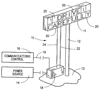
Figure 1 is a perspective view of a representative
variable message display sign according to the
exemplary embodiment of the present invention;
Figure 2 is a diagrammatic view of a variable
message display sign according to the prior art;
Figure 3 is a diagrammatic view showing a
representative character display according to the prior
13
CA 02121297 2001-O1-03
art;
Figure 4 is a diagrammatic view showing the
control and switching system according to the prior art
and used with the character display of Figure 3;
Figure 5 is a front view in elevation showing the
character display module according to the exemplary
embodiment of the present invention;
Figure 6 is a rear perspective view of the
character module shown in Figure 5;
Figure 7 is a cross-sectional view taken about
lines 7-7 of Figure 6 and including the power and data
bus interconnect thereto;
Figure 8 is an enlarged front view in elevation
showing a light-emitting diode array defining a pixel
for the character display of Figures 6-8;
Figure 9 is a cross-sectional view taken about
lines 9-9 of Figure 8;
Figure 10 is a diagrammatic view of a pair of
diode strings-used to form the diode array of Figures 8
and 9;
Figure 11 is a diagrammatic view similar to Figure
B but showing the physical arrangement of the diode
strings of Figure 10;
Figure 12 is a simplified diagrammatic view
showing the interfacing of a plurality of display
modules, such as those shown in Figures 5-7, connected
by means of a data bus to a controller according to the
14
CA 02121297 2001-O1-03
exemplary embodiment of the present invention;
Figure 13 is a side view, partially broken-away,
of the cable forming the data bus of Figure 13;
Figure 14 is a diagrammatic view showing a
representative logic circuit according to the present
invention;
Figure 15 is a diagrammatic view showing the power
supply for the logic circuit of Figure 14;
Figure 16 is a circuit diagram of the address
comparator of Figure 14;
Figure 17 is a circuit diagram of the column
decoder of Figure 14;
Figure 18 is a circuit diagram of the input
enable, output enable and column latches of Figure 14;
Figure 19 is a circuit diagram of the display
power control of Figure 14;
Figure 20 is a generalized circuit diagram of a
pair of pixels in a character display according to the
present invention and showing the feedback capabilities;
and
Figure 21 is a circuit diagram of the feedback
circuitry contained within the logic circuit of the
present invention according to Figure 14.
DETAILED DESCRIPTION OF THE EXEMPLARY EMBODIMENT
A. GENERAL INTRODUCTION
The present invention is directed to a variable
message display sign which is operative to display a
CA 02121297 2001-O1-03
message which may be selectively varied. Generally, a
variable message display sign employs a plurality of
character displays each having a plurality of signal
elements which may be selectively placed in an on and
off state to display a character or image on the
character display, and this selective switching of the
signal elements is accomplished by means of a controller
and logic circuit which process information received by
the controller in the form of the desired message to be
displayed in order to drive the signal elements to
produce the desired message. The present invention
departs from pre-existing systems by eliminating
substantial and complex wiring distinctly
interconnecting each signal element with the controller
by placing a logic circuit in proximity to each
character display and by having a remotely located
controller sequentially address desired ones of the
logic circuits by means of a data bus.
An exemplary embodiment of the physical appearance
of such a sign may be seen in Figure 1 wherein the
variable message display sign 10 includes a sign housing
11 supported on a surface 13, such as the ground, by
means of a support post 12. Sign 10 includes a
plurality of character displays 20 in housing 11, and
character displays 20 operate to selectively display a
desired character to present the desired message.
Variable message display sign 10 includes a controller
16
CA 02121297 2001-O1-03
18 located remotely of character displays 20 and may
conveniently be located an surface 13, for example,
adjacent to the base of post 12 . A power source 14 is
connected to a controller 18, and power is supplied to
characters 20 by means of a power supply cable 22.
Controller 18 also supplies control data to character 20
over a data bus 24. If desired, and is shown in Figure
1, controller 18 may communicate with communications
control 16, for example, over telephone lines 19 in a
manner well known in the art. Communications control 16
can be a centralized control office for multiple signs
and is typically located distantly from variable message
display sign 10, but this is not of course a required
feature of the broad form of the present invention. It
may be noted in reference to Figure 1, that a signal
data bus 24 is used for all of characters 20, and this
feature of the present invention will be described in
much greater detail, below.
In Figure 1, it may also be seen that variable
message display sign 10 is depicted as a traffic warning
sign, although it should be understood at the outset
that the present invention is in no way limited to
traffic control but can be used in any circumstance
where a variable message is desired to be presented to a
viewer. For illustrative purposes, then, it may be
appreciated that a traffic controller may be located at
a centralized office and may communicate with a
17
CA 02121297 2001-O1-03
plurality of controllers 18 for a variety of respective
signs 10 and, by establishing a communications link over
telephone lines 19, can instruct each respective
controller 18 to display a respective message on its
associated variable message display sign 10. Moreover,
communication lines 19 can be used to receive feedback
information to validate the integrity of the displayed
message, as hereinafter described.
B. PRIOR ART TECHNIQUES
In order to understand the departures of the
present invention from the existing prior art, it is
helpful to review the primary features of the prior art
as it relates to variable message display signs. With
reference to Figure 2, then, a typical prior art
variable message display sign 510 employs a controller
518 to individually drive characters 521-524 which are
powered by power source 514. In the prior art, the
number of character displays is selected to be an
adequate number for the maximum length of message to be
displayed. Controller 518 may receive control or
command communications from communications control 516
located distantly therefrom, again for example, over
communication lines 519. In any event, controller 518
has a plurality of data buses in one-to-one
correspondence with the display characters such as data
buses 531-534, respectively associated with characters
521-524. Power is supplied from power source 514.
18
CA 02121297 2001-O1-03
As is shown in Figure 3, the prior art display
such as a representative character display 520 is in the
form of a matrix 560 of signal elements 550 organized in
an r X s matrix of "r" rows and "s" columns. Typically,
in the prior art, such a matrix 560 is a 7 X 5 matrix of
signal devices each of which forms a pixel for the
character display. These signal elements are known to
include a variety of type of structures such as light
bulbs, light-emitting diode arrays, shutter devices,
liquid crystals, and the like. In any event, as is
shown in Figure 4, each signal element 550 is connected
between a voltage or power source 514 to ground with
respective signal element being in series with a switch
580 so that placing a switch 580 in a closed condition
connects the circuit through the corresponding signal
element to turn it into an an-state while an open
condition for switch 580 leaves its respective signal
element 550 in an off-state.
Thus, as is shown in Figure 4, switches
corresponding to signal elements 1,2 1,3 and 7,4 are
closed while switches corresponding to signal elements
1,1,1 and 7,5 are open to correspond to the respective
signal elements located at those row and column
positions. Accordingly, with reference to Figure 3, to
display the character "C" selected signal elements are
in the on-state with the remaining signal elements being
in the off-state. The on-state signal elements for the
19
CA 02121297 2001-O1-03
character "C" are: 1,2; 1,3; 1,4; 2,1; 2,5; 3,1; 4,1;
5,1; 6,1; 6,5; 7,2; 7,3; and 7,4.
According to the prior art, the representative
data bus 530 for each pixel typically includes a
discreet wiring connector interconnecting each
respective signal element 550 to controller 516 so that,
with reference to Figures 3 and 4, thirty-five such
wiring connectors 590 would be used to control a single
character 520. Where a variable message display sign
has ten characters, this would result in the use of
three hundred fifty lead wires to communicate the
information to each pixel on a one-to-one
correspondence. This wiring is accordingly complex,
expensive and difficult to maintain.
C. PHYSICAL STRUCTURE OF THE CHARACTER DISPLAY
ACCORDING TO THE EXEMPLARY EMBODIMENT
OF THE PRESENT INVENTION
According to the present invention, then, an
improved character display is provided as shown in
Figures 5-11 and the simplified physical structure of
the variable message display sign is diagrammed in
Figure 12 with the data bus shown in Figure 13. With
reference to Figures 5-7, it may be seen that character
display 20 (used in sign 10 of Figure 1) includes a
support panel 32 having a front surface 34 and a rear
surface 36. Support panel 32 supports a plurality of
signal elements 50 which are disposed on the front
CA 02121297 2001-O1-03
surface 34 with these signal elements 50 being
preferably arranged in a matrix of seven rows "r" and
five columns "s". Also as described more thoroughly
below, each signal element 50 has feedback circuit
elements 52 associated therewith in one-to-one numerical
correspondence.
With reference to Figures 6 and 7, it may be seen
that a logic circuit 40 is formed on circuit board 41
that is mounted to and supported by support panel 32 in
spaced parallel relation to rear surface 36 at a central
portion of support panel 32. Logic circuit 40 includes
a plurality of logic components 42 and a connector 44 to
interconnect a logic circuit to mating connector 46 on
data bus '24. A power connector 48 is also disposed on
rear surface 36 of panel 32 and cooperates with a
connector 49 on power supply cable 22 which is
preferably set at twenty-four volts DC. Printed
circuitry (not shown) may be disposed on support panel
32, preferably on rear surface 36, to~interconnect the
electric components mounted thereto.
A representative signal element 50 is shown in
Figures 8 and 9 where it may be seen that each signal
element includes an array of light-emitting diodes 54
which are organized in rows and columns and have their
diode leads 55 directly wired to support panel 32 which,
as noted above, is in the form of a circuit board that
provides the electrical interconnects between diodes 54
21
L,
CA 02121297 2001-O1-03
forming the signal elements 50 and connects logic
circuit board 41 by means of multi-pin connects 56 and
58, shown in Figure 7.
With reference to Figures 10 and 11, it may be
seen that diodes 54 are preferably organized in at least
two strings or groups 60 and 62 wherein the respective
diodes 54 are electrically connected in series with one
another and with a respective 191 ohm resistors 70 and
72. Resistors 70 and 72 are selected according to the
characteristics of diodes 54 in order to
regulate the current through the signal circuit (e. g.,
the diode strings) to help stabilize the current. Each
of groups 60 and 62 are electrically connected in
parallel with one another so that, if one diode 54 burns
out and creates an open circuit, the respective pixel
will remain operable but with less intensity. Diodes 54
in groups 60 and 62 are arranged, as is shown in Figure
11, so that there is at least one group 60 diode and at
least one group 62 diode in each row of the array 51 and
at least one group 60 diode and at least one group 62
diode in each column of array 51. Thus, for
representative purposes in Figure 11, the group 60
diodes are represented by squares and the group 62
diodes are represented by triangles.
Turning to Figure 12, it may be seen that the
controller 18 is interconnected to each character
display 20 by means of a simple data bus 24 which mounts
22
CA 02121297 2001-O1-03
the connectors 46 that are securable to respective
logic circuit boards 41 of logic circuits 40 at
respective addresses A1, A2, A3, . . .An. Since it is
desirable that each of character display 20 be
identical, the unique character address A1, A2, A3,
...An is hard-wired by each interconnect cable 24 and it
associated connector 46, as described more thoroughly
below, although other address techniques may be
implemented without departing from the scope of the
present invention. Moreover and as described below,
controller 18 operates to sequentially and selectively
address the logic circuits, the character displays
residing at each individual address so as to load those
logic circuits with the display data corresponding to
the desired character to be displayed by the respective
character display.
The structure of data bus 24 is best shown in
Figure 13 where it may be seen that data bus 24 includes
a plurality of wire leads for carrying control signals,
data signals, feedback signals and ground connections.
With reference to Figure 13, it may be seen that
grounding wires 80,81' provide an electrical ground for
data bus 24 and for the hard wiring of the character
addresses while five wires 81 form an address bus for
addressing a selected one of the character displays and
three wires 82 form a column select bus for carrying
column address data. Seven wires 83 define a data bus
23
CA 02121297 2001-O1-03
for carrying display data. Seven wires 84 form a
feedback bus. Finally, wire 85 carries a clock or
strobe pulse while wire 86 carries a pulse width
modulation pulse for controlling the duty cycle of each
character display. It should be understood that the
number of grounding wires, address wires, data wires,
feedback wires and the pulse-width modulation may be
changed according to the needs of a particular variable
message display signal. Moreover, certain features are
optional without departing from the broad scope of this
invention. For example, if duty cycle control is not
desired, the pulse-width modulation wire 86 may be
eliminated entirely. Address wires 81 may be increased
or decreased based upon the number of character displays
desired to be controlled by controller 18. With five
such wires 81, of course, thirty-two (25) display panels
may be addressed. Similarly, the number of wires in the
column bus may be varied depending upon the number of
columns in the character display matrix. Where three
column wires are provided, eight (23) columns can be
addressed. The data wires 83 are in one-to-one
numerical correspondence with the number of rows i.n the
matrix for the character display as are the feedback
wires 84. Of course, if no feedback capability,
described below, is desired, feedback wires 84 may be
eliminated entirely. Where feedback is provided, the
number of wires 84 should equai the number of wires 83
24
CA 02121297 2001-O1-03
for carrying feedback data in one-to-one correspondence
with the row data.
D. CONTROL AND LOGIC CIRCUITS
The overall control and logic circuits for
variable message display sign 10 is diagrammed in Figure
14. Here, it should be appreciated that controller 18
is located remotely from the character displays and is
operative to produce an address signal containing
character address data for identifying an addressed
character display so as to eliminate the need to provide
individual electric leads to each pixel. This address
signal is carried by address bus 81 which is connected
to an address comparator 100 which receives, as its
inputs, the address carried by address bus 81 and a
local address 101 corresponding to the unique local
address for its respective character display. Upon the
occurrence of a strobe pulse on strobe wire 85, address
comparator 100 compares the local address and the
address data to see if they match, as is shown in block
102. If the character address data on address bus 81
does not match the local address, all pixel columns of
the associated character display are activated for
display, as at 103, according to the display power
control 104 which in turn is governed by the pulse-width
modulation signal on lead 86. However, where a match
occurs between the local address and the address data,
CA 02121297 2001-O1-03
address comparator 100 recognizes that its logic circuit
and the associated character display are being addressed
by controller 18 and generates a match signal at 110
that is transmitted to column decoder 120. Disable
display 130 operates to generate a disable signal
preventing the signal elements on the associated
character display 20 from reacting to changes in row and
column display data, other than as may occur during
feedback testing described below.
Controller 1B generates a set signal containing
set address data for identifying an addressed set of
signal elements, such as a selected column, and this set
signal is input to column decoder 120. Upon receipt of
a strobe pulse from strobe 85 and in the presence of
match signal 110, column decoder decodes the binary
column information from column select bus B2 at 121 to
produce an enable signal 122 which is presented to an
input enable 124 and an output enable 126. Input enable
124 produces_an input enable signal for column latches
251, 252, 253, 254 and 255 according to the column data
carried by data bus 82. Thus, for example, if column
address data corresponding to column three is carried on
columns selected bus 82, column decoder 120 and input
enable 124 enable the input 263 of column latch 253 so
that latch 253 latches the display data carried by
display bus 83. Simultaneously, output enable 126
triggers the output 272 of latr_h 252 so that latch 252
26
CA 02121297 2001-O1-03
causes the character display to display column two, as
shown at 282. This display by latch 252 occurs for the
duration of the strobe pulse 85 connected to column
decoder 120 so that the display of the selected column
enabled by output enable 126 occurs for a very short
interval sufficient enough, however, to allow the
associated feedback circuit 292 to read the status of
the signal elements or pixels in display column and to
provide this information on feedback bus 84 so that the
data is returned to controller 18 for testing the
integrity of the display.
From the foregoing, it should be appreciated that
the address data carried by address bus 81 addresses
allows controller 18 to address the specific character
display associated with a logic circuit having a unique
character address therefore. This allows the logic
circuits to be located in close proximity to its
respective character display with the controller located
distantly from the character display. Once a logic
circuit is addressed, its associated character display
is disabled, and the latches 251-255 are activated
sequentially to latch the column or "addressed set" data
then residing on data bus 83. Thus, controller 18
addresses a selected logic circuit and then cycles
through all of its column latches to load the
appropriate display data in each latch according to the
row in the column. Between strobe pulses, the
27
CA 02121297 2001-O1-03
controller selects a new column and alters the data for
that column.
By disabling the overall character display, the
character display is blank. After loading one column
into its respective data latch, controller 18 addresses
a subsequent column. At this time, though, output
enable 126 activates that data latch for a preceding
column which is already been loaded so that the data
latch is enabled to display, for the duration of the
strobe pulse, the feedback data derived from the
monitoring of the signal elements corresponding to the
preceding column. This feedback data may be processed
by the controller to compare the feedback data from the
intended signal display data for that column to
determine whether it is valid. In other words, when
data corresponding to the desired on/off states for each
signal element in a selected column is being latched, a
different column is being tested for integrity of the
previously latched data. As discussed below, not only
does this allow for testing of the integrity of the
display data, but also allows an operator to selectively
and remotely test to determine the proper functioning of
the signal elements and their associated switches which
comprise the entire message display.
With reference to Figure 15, it may be seen that
the voltage to drive logic circuit 40 may be obtained
from the power voltage "Vo" provided over power line 22.
28
CA 02121297 2001-O1-03
Preferably Vo is preferably approximately twenty-four
volts DC, and it is desired to operate the logic circuit
at "V+" which is preferably about five volts DC. To
derive V+, a power supply circuit 300 is associated with
each logic circuit 40 and includes a voltage divider 301
in the form of a circuit chip (LM7805) which receives
the Vo input through resistor 302 which is preferably
200 ohms. The input of chip 301 is grounded by means of
capacitor 303 and the output of chip 301 is grounded by
capacitor 304. Capacitors 303 and 304 are respectively
1.O~~and 10~ With this configuration, chip 301
.Sl~~~~ provides a five volt DC output as V+.
Figure 16 shows hard wiring for the unique address
and the functioning of address comparator 100. Here, it
may be seen that connector 46 of interconnect cable 24
has a plurality of ground wires 80 which may be
selectively severed to provide a binary pattern. Thus,
leads 310 and 311 are connected to ground and inputs 80'
can be thus configured to provide a unique address code
at the address comparator inputs 331. Leads 81 of
interconnect cable 24 allow controller 18 to place an
address on address bus 81 by pulling down leads 321 and
323 to ground with the remaining leads remaining high
due to the connection to V+ through connector 44. Thus,
when controller 18 places the appropriate address on
leads 81, this character address data will match the
hard wire address provided by connector 46.
29
CA 02121297 2001-O1-03
Connector 46 is connectable to connector 44 of
logic circuit 40 and provides the inputs for comparator
chip 330 which is preferably a 74HC688 or any other
comparable binary comparator. Inputs 331 and inputs 332
of chip 330 are connected to the pins of connector 44 by
means of lOk ohm resistors 333. The pins of connector
44 corresponding to inputs 331 are also connected to
through 100k ohm resistors 334 and the pins of connector
44 associated with inputs 332 of chip 330 are connected
to V+ by means of lOk ohm resistors 335. When the
hardware address on inputs 331 matches the controller
address on pins 332, comparator 330 outputs a pair of
signals M and M- which have opposite values from one
another and which each switch to their opposite state
depending on whether an address match occurs. If an
address match occurs, the output M- of chip 33 is low;
the opposite signal "M" is provided by NAND gate 338.
Thus, M is high at V+ when an address match occurs.
When there is no address match, M- remains high and M is
correspondingly low.
Turning to Figure 17, column decoder 120 is shown
to include a processing chip 340 which is preferably a
74HC138 microchip or equivalent decoder. Chip 340 has
inputs 341 which receive the column address data from
wires 82 by means of the connection of connector 44 to
connector 46. Accordingly, inputs 341 are connected to
the pins of connectors 44 through lOk ohm resistors 342.
CA 02121297 2001-O1-03
The pins of connector 44 corresponding to inputs 341 are
also connected to V+through l.Ok ohm resistors 343.
When both the strobe pulse S and the signal M- are
present, chip 340 produces one of a possible six outputs
L1 - L6 depending upon the binary pattern from wires 82.
Thus, where the respective logic circuit 40 is
addressed, column decoder 120 acts to address a selected
column in its associated character display according to
the column address data. The outputs of chip 340 are
high except for the decoded column which is pulled low.
Inverters 344 invert the outputs of decoder chip 340 so
that the addressed one of signals L1 - L6 is at V+ while
all others of Ll - L6 are low (ground). L1- through L6-
are the complements of L1 - L6.
Figure 18 shows the operation of the data latches
25
corresponding to each column. Depending upon which of
outputs L1 - L6 is generated by column decoder 120, that
high signal is applied to the input respectively of data
latches 351=355. The seven inputs of each of data
latches 351-355 are connected to the outputs of buffer
chip 360 which may be a 74HC540 or equivalent microchip.
The inputs of buffer 360 are connected to the
corresponding pins of connector 44 through lOk ohm
resistors at 361, and the corresponding pins of
connector 44 are also connected to V+ by means of lOk
ohm resistors 362. Data carried by data bus 83
accordingly passes through buffer 360 and is presented
31
CA 02121297 2001-O1-03
to each of data latches 351-355. However, only the data
latch corresponding to the activated column signal Ll -
L6 acts to latch the data, with the column pulse only
occurring for the duration of the strobe. As noted
below, L6- is used only for feedback.
For example, if column three is to be addressed,
column decoder 120 produces high on L3 and a low on L1,
L2, and L4 - L6 so that the row data corresponding to
the data on data bus 83 is latched at the input of data
latch 353. Simultaneously, however, output L3 is input
into AND gate 372 so that the output of data latch 352
is activated to produce a switch signal for each signal
element (1,2; 2,2; 3,2; 4,2; 5,2; 6,2; and 7,2~ which
signals correspond to the previously latched data when
input enable signal L2 was present. Latches 351-355
accordingly each have an AND gate 371-375 connected to
its output enable. The switch signals are thus output
through 2.2K ohm resistors 376 connected in series to
the outputs of each of data latches 351-355.
As noted above, except for testing the integrity
of previously latched column data, the character display
corresponding to the addressed character is forced into
an off state when it is receiving new address data.
This is accomplished by the control circuit shown in
Figure 19 which includes an NAND gate 380 which has a
first input connected to V+ through a lOk ohm resistor
381 and a lOk ohm resistor 382 connected in series with
one another. The inverted pulse width modulation signal
32
CA 02121297 2001-O1-03
from controller 18 is connected between resistors 381
and 382 so that, in the presence of the pulse switch
modulation signal, the inverted pulse switch modulation
signal goes low so that the first input of NAND gate 380
is low. The second input of NAND gate 380 is connected
to the signal M-. Thus, when the module is addressed,
the output of NAND gate 380 is always high. However,
when the module is not addressed, M- is high and the
output of NAND gate 380 is the inverted PW- signal which
is simply the same as PW, that is, the pulse width
modulation signal from controller 18. The output of
NAND gate 380 is connected to the gate of transistor 390
through 750 ohm resistor 391. When this output is low,
transistor remains in an off condition but transistor
turns on when the output of NAND gate 380 is high. The
resulting control signal DP therefore switches according
to the pulse modulation when the character module and
its associated logic circuit is not addressed. When
addressed, however, DP is always high so that the
feedback will operate. Preferably the pulse-width
modulation has a ten millisecond period and can be
controlled for 0~ - 100 (full power). It should be
understood that this can be adjusted as desired.
E. FEEDBACK CIRCUITRY
The present invention also includes new and useful
feedback circuitry for the variable message display sign
33
I,
CA 02121297 2001-O1-03
described above. In order to best understand the
feedback circuitry, reference is first made to Figure 20
which is a diagram of a portion of a character display
as above described. Here, each signal element 50,50' is
defined by a first diode array 60,60' connected in
series with resistor 70,70' and a second diode array
62,62' connected in series with a second resistor 72,72'
with these two diode array circuits 60,62 and 60',62'
being connected electrically in parallel to one another
between a switched power source VO and ground.
Switching is accomplished by means of a switch
transistors 400,400' which have their collectors
connected to a respective signal element 50,50' and
their emitters connected to ground through an eighteen
ohm resistor 401,401'. The base of each switching
transistor 400,400' is connected to ground through a lOK
ohm resistor 402,402'. Moreover, the base of transistor
400 is connected to the output 1, 1 of latch device 351
while the base of transistor 400' is connected to output
2,1 of latch 351.
Thus, it may be seen in reference to Figure 20,
that signal elements 50,50' correspond to the first row
and the second row signal elements in column one of the
associated character display. Signal elements 50,50'
are connected in parallel to one another between ground
and voltage Vo, and are connected to voltage Vo through
a switching transistor 410 which may be an MJE271
34
CA 02121297 2001-O1-03
transistor. The base of transistor 410 is connected to
Vo through a lOK ohm resistor 411 and to pulse control
signal "DP" through lOK ohm resistor 412. The collector
of transistor 410 is directly connected to Vo and also
to ground through a 1000 micro-farad capacitor 413.
Accordingly, when a pulse signal is present on the base
of transistor 410, it turns on so that power is supplied
to power line 415. Accordingly, when the switching
transistors, such as transistors 400,400' are in an open
state, the signal device 50,50' will remain off.
However, in the presence of an enable input signal at
1,1 or 2,1, the respective switching transistor 400,400'
will switch into a closed state completing the circuit-
to-ground thereby allowing the respective signaling
element 50,50' to move into an on-state when in an
operative condition.
Feedback transistors, such as feedback transistor
420,420' have their respective bases connected to the
emitters of switching transistors 400,400' and monitor
the voltage present at the emitter. For example, if
switching transistor 400 is in an open state, no voltage
is present on the base of transistor 420 so that the
output FB 1,1 remains high. However, if switch 400 is
closed and switch element is operative, sufficient
voltage is present on the base of transistor 420 so that
it switches thereby allowing FB 1,1 to go low indicating
that switch elements 50 are properly functioning. If
CA 02121297 2001-O1-03
one of the diode arrays 60, 62 ceases to function, such
as the burnout of the one of the diodes in the
associated diode array, then the resistance increases
and the current through the circuit decreases. Thus,
transistor 420 does not turn on and feedback signal FB
1,1 remains high. Likewise, should the switch element,
such as switch transistor 400 fail by shorting, signal
element 50 is always on and feedback FB 1,1 is always
low regardless of the status of input signal 1,1.
The outputs of the feedback transistors 420 for
each given row are connected together to simplify the
feedback circuit. The outputs of each feedback
transistor in a given row, then, is represented as
feedback signals F1-F~ in Figure 21. Each of these
signals is connected to the inputs of a feedback latch
356 through lOK ohm resistors 430 and respectively to V+
through 100K ohm resistors 431. The outputs of feedback
latch 356 are connected to connector 44 to the pins of
connector 44 through resistors 432 to provide the
feedback data connected to the pins of connector 46 and
thus to feedback bus 84.
The output of latch 356 is disabled when the
respective module is not addressed since M- is high.
When the module is being addressed, M- is low. The
output of NAND gate 433 is therefore low in the presence
of strobe pulse "S" since M is high; the output is high
in the absence of the strobe pulse. Inverter 434
36
CA 02121297 2001-O1-03
inverts this signal, however, so that the resulting
input enable to latch 356 is switched according to the
strobe pulse when the module is addressed.
With reference again to the preferred exemplary
embodiment described especially in reference to Figures
14-19, the integrity of the signaling devices of each
pixel may be tested by causing controller 18 to
sequentially blank each column of each character display
while monitoring the feedback through feedback latch
356. If any signal element is improperly operating, the
malfunction will appear on the row data containing the
malfunctioning switch device for each column of that
character display. Thus, the operator will know that
one of the switch devices in the identified row is
malfunctioning so that the character display module can
be replaced and repaired.
On the other hand, controller 18 may sequentially
instruct each column to light up each pixel in its
corresponding rows. Here, the feedback signal will
indicate whether any pixel is "burned-out" or of a
diminished capacity (where parallel signal elements are
employed). Should the feedback data indicate a high
condition for the feedback transistor of a pixel, then
the operator will know that the signal device occupying
that column and row position is defective. Again, the
character module may be replaced and repaired.
37
CA 02121297 2001-O1-03
According to the general method of the present
invention, a method for controlling a plurality of
character displays is provided wherein each character
display has a plurality of signal elements that are
individually switchable between on and off states in
order to produce a pattern of a desired character.
These signal elements are organized in a plurality of
sets, and the method comprises the control of these
signal elements. The method includes the first steps of
providing a logic circuit proximate to each character
display with each logic circuit including a memory
operative to store display data for each of the
associated signal elements of each of its associated
sets, providing a unique address for each such logic
circuit, providing a controller for each logic circuit
located remotely thereof and interconnecting the logic
circuits and the controller by means of a common bus.
The method further includes the step of placing a
character address on the bus and comparing the character
address with the unique addresses for each logic circuit
so that an addressed one of the logic circuits is placed
in a condition to receive display data with remaining
ones of the logic circuits inhibited from receiving
display data. A set address is also placed on the bus
to identify a selected one of the sets of signal
elements so that the memory associated therewith is
placed in a condition to receive the display data with
38
i,
CA 02121297 2001-O1-03
all other memories of the address logic circuit being
inhibited from receiving display data. Also, display
data is placed on the bus corresponding to each of the
signal elements of the selected set, and the display
data is loaded into the memory associated with the
selected set of the address logic circuit. The steps of
placing character address data, set address data and
display data on the bus is then repeated until the
memories of all of the logic circuits are loaded with
display data for their respective character displays.
Said character displays are, of course, powered so that
the signal elements thereof are switched to display the
pattern according to the display data.
Preferably, the steps of placing the character
address, the set address and display data occurs
simultaneously, and the method includes the step of
providing a clock or strobe pulse which causes the data
to be processed as described above. In between the
clocking pulses, the controller acts to vary the display
data as needed and the addressed logic circuit and/or
set of signal elements. The method can include the
inhibiting of any display of data by the character
display associated with the addressed logic circuit.
Also, the method may include the feedback to the
controller of feedback test data wherein the integrity
of the display pattern far each set of signal elements
is compared with the intended display data for the
39
CA 02121297 2001-O1-03
y
signal elements of the selected set. Preferably, the
method includes the step of loading display data for one
set of signal elements while testing the data previously
loaded for another set of signal elements. This method
may also include any step inherently practiced by the
apparatus and control circuitry described herein.
Accordingly, the present invention has been
described with some degree of particularity directed to
the exemplary embodiments of the present invention. It
should be appreciated, though, that the present
invention is defined by the following claims construed
in light of the prior art so that modifications or
changes may be made to the exemplary embodiment of the
present invention without departing from the inventive
concepts contained herein.