Note: Descriptions are shown in the official language in which they were submitted.
21 21 347
BACKGROUND OF THE INVENTION:
Connectors designed for avionics, military, and
other high performance applications, have recently included
contacts wLth circuit components. For example, contacts have
been used which include Zener diodes or -metal oxide varistors
~MOV's) for dissipating to ground, high energy pulses that may
be induced on tlle contact. Other contacts have been designed
wi~h filters such as pi filters (an inductor between two
capacitors) that block .signals above a predetermined frequency
1~ such as high frequency noise. Although a connector user can
specify to the manufacturer the particular type of connector
he requires, specifylng which type of component contacts lie
at particular locations, this rnakes it difficult for the user
to try different configurations and requires the manufacturer
to custom make each different type of connector. ~f the
custorner, or user, could easily produce his own connector from
supplied parts, this could reduce the manufacturing costs and
increase the ability of the user to modify his own connector.
IJK-A-201480~ represents this connector art.
Ground planes currently used in connectors to ground
some of tlle contacts, can include a thin plating on an
insulator or a sheet metal ground plane. The plated ground
plane cannot carry high current surges and the plating cost is
considerable. Current sheet rnetal ground planes are bonded to
insulators to assure that the spring fingers at the outer edge
of the ground plane will lie stabiy within a connector shell.
The cost of bonding the sheet metal ground plane to an
insulator adds to the cost of the connector. ~ ground plane
and insulator assembly which could be constructed at a low
,~.,
. ~
1 761~2-2
21~1347
cost would be of value.
SU~MARY OF THE INVENTION
In accordance with the ~resent invention there is
provided a connector whicll has a conductive shell, a holder
lying in said shell with said holder having forward and
rearward ends and a plurality of contact-receiving holes
therein, and a plurality of contacts each lying in one of said
holes with each contact having forward and rearward ends lying
~dlacent to corresponding ends of said holder and with each
lG cGntact having a rniddle portion, wherein said holder includes
a conductive ground plane extending across the inside of said
shell and having an outer edge portion electrically grounded
to said shell and a plurality of apertures lying at said
contact-recelving holes and having pro~ecting fingers
extending into said apertures for engaging said contacts with
said finger formed to engage a cylindrlcal portion of pre-
cleterrnined diarneter, characterized by; each of said plurality
of contacts is individually removable and replaceable and is
interchangeabiy installable in any of said plurality of
~O contact-receiving holes, and each of said plurality of
cont~cts includes a conductive element extending along the
entire length o~ the contact and having an element middle; a
first group of said contacls including component contacts with
eac}-l including a ci.rcuit component mounted on said element
middle and a substantially cylindrical conductor of said
predeterrnlned diameter e~tending a~out said element middle,
sa1d comporlent havin~ a first terminal connected to said
element middle and a seconcl terminal connected to said
c-ylindrl.cal ~onductor; a second group o~ said contacts
~, la 76132-2
2121347
including a feed through contact having only insulation
surroundiny the element middle.
In accordance with the present invent.ion there is
also provided a connector con~prisirlg; a conductive shell; a
hol-~,er lying in said shell, said holder having forward and
rearward ends and a plurality of contact-receiving holes
therein exterldirlg between said ends, said holder including a
ground plane having a plurdlity of apertures at the positions
of said holes and having a plurality of fingers proiecting
into eacll aperture; a plurality of contacts which are
individually removable and replaceable in said holder holes,
said contacts being interchangeably mountable in each of said
plurality of holes, with each contact having a conductive
element with opposite ends and a middle, said plurality of
contacts includirlg at least one component contact and at least
one passive contact; sai~ component contact having a circuit
componerlt with a first termirlal connected to said element
middle and a second terminal, said component contact also
havi.ng a conductive cylinder lying about said element middle
and connected to said second terminal, said conductive
cylinder being of 3 diameter to engage a plurality of said
ground plane fingers; said passive contact is devoid of a
circuit component but has a contact middle with an insulative
outer diameter large enouyh to also engage a plurality of said
ground plane firlgers.
In accordance with the present invention there i.s
~urther provld~d a connector assembly comprising first and
second connectors t~,at a.re connectabl.e in tandem, each ha-~ing
a shell, a holder lying in the corresponding shell and having
~,..
~Y~
k- lb 761~2-2
21 21 341
a plurality of contact-receiving holes and with said holder
having a ground plane with apertures lying at each hole and
with a plurality of fingers proiecting into each aperture, and
a plurallty of contacts each mounted in one of said holes;
each of said contacts includes an elongated c~onductive elernent
with first and second opposite ends forming first and second
encls of said contacts arld with an element middle lying within
one of said ground plane apertures, said contacts of each
connector being interchangeably rnountable in any of said hoIes
of the holder of that connector; at least a first contact of
each connector incluclirlg a circuit component with a first
terminal mechanically and electrically connected to said
element l-niddle, and also including a conductor connected to
said second terminal with said conductor having a largely
cylindrical outside of a diarneter to ~e engaged by a plurality
of fingers of said grollnd plane; said connectors being
connected in tandem, witll said second ends of said contacts of
said first connector forming sockets and with said first ends
of said contacts of said second connector forming pins
received in said sockets of said contacts of said first
connector-, anc3. with said firs'r contact.s of each said first and
second connectors being connected in tandem, whereby to enable
a more comple~ circuit to lie along a pair of tandem-connected
contacts.
In accordance with one embodiment of the present
~.
~.f~
ic 76132-2
W O 93/08622 2 1 2 1 3 ~ ~ PC~r/US9t/07659
invention, a connector is provided of the type that has at
least one component contact which includes a component
mounted on a conductive element, which is versatile and of
low cost. The connector is of the type that includes a
ground plane with contact-passing apertures through which a
contact can be inserted so a middle portion of the contact
is connected to the ground plane. A first group of contacts
comprise component contacts, each including a circuit
component mounted on the middle of the conductive element
and a cylindrical conductor of a diameter to engage ground
plane fingers in the ground plane aperture. A second group
of contacts comprise feed through contacts, each including
insulation surrounding the middle of the element, with the
insulation having a largely cylindrical exterior of a
diameter great enough to engage fingers of the ground plane.
A third group of contacts comprises ground contacts, each
including an enlarged conductive element middle diameter
great enough to engage fingers of the ground plane. The
feed through and ground contacts are interchangeable with
the component contacts.
The ground plane is stamped or otherwise formed of
a sheet of metal and has slots. Forward and rearward
insulators lie facewise against opposite faces of the ground
plane, with one insulator having tabs that project through
the slots in the ground plane and into slots in the other
insulator where the tabs are tightly captured to hold the
assembly together.
A pair of connectors with interchangeable contact
can be connected in tandem, with each contact of one
connector lying in tandem with a contact of the other
connector. This enables each pair of tandem contacts to
provide a more complicated circuit, as where one provides a
diode for dissipating most of the energy of a pulse, and the
other provides a filter for further dissipating the pulse~5 energy at certain frequencies.
, . ,
, .
W093/0~22 z~ 3 ~ ~ PCT/US91/07659
The novel features of the invention are set forth
with particularity in the appended claims. The invention
will be best understood from the following description when
read in conjunction with the accompanying drawings.
BRIEF DESCRIPTION OF THE DRAWINGS
Fig. 1 is a front isometric view of a connector
constructed in accordance with the present invention.
Fig. 2 is a front elevation view of the connector
of Fig.l.
Fig. 3 is a view taken on the line 3 - 3 of Fig.
2.
Fig. 4 is a sectional view of the diode contact of
Fig. 3.
Fig. 5 is a sectional view of the filter contact
of Fig. 3.
Fig. 6 is a sectional view of the feed through
contact of Fig. 3.
Fig. 7 is a sectional view of the ground contact
of Fig. 3.
Fig. 8 is an exploded isometric view of the holder
of Fig. 3.
Fig. 9 is a partial sectional view of a connector
arrangement constructed in accordance with another
embodiment of the invention.
Fig. 10 is a sectional view of a varistor contact
which can be installed in the connector of Fig. 3.
DESCRIPTION OF THE PREFERRED EMBODIMENTS
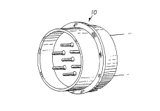
Fig. 3 illustrates a connector 10 which includes
a conductive shell 12 and a holder 14 lying within the
shell. The holder has forward and rearward ends 16, 18 and
a plurality of contact-receiving holes 20. A plurality of
contacts 22A - 22D lie in each of the holes, with each
RC\/. \~o~:E~ E~;CHE~ J- 3~ 3 1'' ~4 ~ 17'~ +49 8'J ~'~39'34~ 4
21 ~I~4~
ccntact having forward and rearward ~nd¢ 30A - ~00 and
32A - 3~D (~ig~. 4 - 6). ~ach ~ontact ha8 a middle portion
such as 34~ lying between th~ opposite end~ of the contact.
The holder 14 includes a conductlve ground plane
~0 extending acr~ss the in~ide of the shell 12, and havln~
a radially outer edge pcrtion 42 formin~ multiple tanqs ~
that engaqe the inside of the sheil, 90 the ~ell and ground
p~ane are at the ~am~ potential (usually g~ound potential).
The ground plan- has a plurality o~ apsrt~r-s 46 lying at
the contac~-r-ceiving holes 20 o~ tho holder, and has a
plurality of projecting f~ngers 48 at edch aperture. The
projecting fing-rs ex~end lnto the ~perture, and engage the
middle portions 3~A - 34D of the contact~. The fingers are
designed to engage contacts who~e middle portion~ have an
lS outside diametQr D wit~in a prsd-t~r~ined range of
diameter~. The middle portions of all of the contacts
Freferably have an outside diameter within t~is range.
Each of the contacts i installable ~n any of the
pluralit~ of contact-receiving holes. Each of the contac~s
ca~ be removed and in~talled in t~e hole pr~viously occupied
by another contact, ~o the contact~ ara int~rchangeably
installable in any of the holes. Rear release retainers 49
hold each contact in pl~ce.
Figs. 4 - 7 ill~strate details of each o~ the four
contacts Z2A - 22~. All of the contacts include a
conductlve element 52A - 52D extending along th~ ontire
lengt~ of the contact. Tha ~orward end8 30A - 300 dnd
rearw~rd en~ 32A -3ZD o~ each of the conductive elements
and contacts are pre~erably the 8ame, but the elem-nt
midd~es 54A - ~4D may b~ different ~or dif~erent contact~.
Fi~. 4 illustrates a diode 50ntact 22A which
includes a ~en~r diode 60 ~ounted on a plat~or~ 62 ~ormed in
the elemen~ middle 54A, with one ter~inal of the diode
mechan~cally and electrically connected to the platform 62.
S~ T
~C~ EP.~-~fl.. E.~CHE.\i ' ~ 3-9~3 1 ' .~.~ : I ''()1 ~'~5 1~'~9; +4~ 8~ 3994~65: ~ ~
~ 1 3 ~ ~
s
The contact also include~ a ground clip 64 with an cuter
part 68 lyin~ at the outside of the contac~ middle portlon
34A an a diameter ~. The clip 64 ha~ an arm 66 that extends
inwardly to a terminal of the diode 60 that ia oppooite the
contact element platform ~2. A q~ntity of molded
insulation 69 surrounds the eloment mlddle S4A o~ the
conduct~ve elem~nt 52A. The purpose o~ the in~ulation is to
protect ~he diod~ 60 fro~ mechanlcal dama~c and to form a
cylinder with diameter D. Wh~n ~ ~igh voltage pul~e travels
along t~e con~a~t, the Zener diod~ breaks down and allows
most of the ~nergy o~ the pulse to pas~ through the ground
c~ip 64 and through the groun~ plane engag~d therewith to
ground. This type cf diode contact 22A ha~ been sold by
applicant for several year~.
Fig. 5 illustrate~ th~ filter contact 22~. It
includes a ferrite bead ~0 surr~nAi~q the elem~nt ~iddl~
~4B of the conductive ele~ent 52~, and a pair o~ capacitors
72, 7~ sur~ounding ~he elQment middle and lyin~ at oppos~te
ends of the ~errite bead. A conduc~ive cylinder ~4'
surrounds the fe~rita and capacitor circu$t components.
Each capacitor has an inner terminal elec~rlcally connected
tc the conductive element ~iddle and the outer tsrm$n~1
connected to the conductive cylinder 74. Applican~ prefer~
to use discoidal capac$tors, which h~ve conduc~ive plates
~5 extending perpen~icular to the length of the conduct~ve
element. It may Be nc~Qd ~hat the ferrite bead 70 do~s not
have ~o be electrically connected to anything, and
prefer~bly doe~ not touch the conductive cylinder 74 to
a~roid a ~oderate resistance direct conn~ction of t~e
conductive element and conductiYe cylind~r through the
ferrite bead. It may be noted that both the diote contact
22A and filtQr contact 22B may b~ con~ider-d to ke corronent
cantacts in that each includes a cir~u~t component. A
circuit component is a device such as a diode, capacitor,
SUB~ I I i UTE SHEET
RC\~ E8~ 11 E~CHE.\ ') . 19- '3-~:3 L" 5~ 25 17-~9 ) ~9 89 ''~9~*~a~
~1~'13~
inductcr, varistcr or resistor tllat a~ects changlng
currents pa~sing therethrough, ot~er than ra-rely al ways
cGnducting or always not conduc~ting them. T~e circuit
component can ~e any shape such ~ a chip diode ~r a tu~ular
vari stor.
Fig. 10 illustrates a varlstor c~ntact 22E which
can sometimes be u~ed instead o~ the diod- contact o~ Fig.
4 to dissipate high energy pul~es. The varist~r contact 22~
~ncludes a circuit cer~ronent ~o~ed by a vari~or 75 maunted
0 on an element ~iddle 54E. The tu~ular var~stor ha6 been
metalized, so it has mf~tal layers 16, 78 at it:~ inner and
outer diameter~. The inner lay~r 76 contact~ the e}sment
middle 54E wh~le t~e outer layer 78 cont~ct- finger~ Or the
gro~md p~ ane when t31e vari-tor contac~ i~ install~d in th~
15 connector.
F, g. 6 illust~at-s the foed through contact 22c
~hich includQs ~ quan~i~y of insulation 80 surrounding the
elernent middle 54C ~f ~che ~onduct~ve elem~nt 52C. The
~adially ~uter su~fac~ 82 of the insulation is subs~antially
20 cylindrical, and has a~out the same diamet~r as the outside
diameters of the ground clip ~4 and conductive cylinder 74 '
of the contact~ of ~ 8. 4 and 5. The purpose Or th~
insulation 80 is tO i~ol~te the conductiv~ ele~ent 52C from
the f ingers of the ground plane to avoid contact with tne
25 ground plane. The ~uter di~meter o~ t~le in8ulat~0n ~o ia
preferably lar~e enough to engage the f ingers of the ground
plane tr.at exten~ed to the aperture through which ~he feed
- throu~h contact ~x~ends. ~ enable- the fingers of the
ground plane to sta~$1ize the position of t~e ~iddle of the
feed t~rough contact and prevent it fro~ "rattling". In
addition, this allow~ a mold used to ~old in6ulat~0n at the
middle portion 34A o~ the diode contact, t~ bQ u~ed to mold
the insulation at the middle p~rtlon 34C af the feed through
contact.
S~ T
~C'~ EP4~ HE~ ' 19- .~ 3, L'' 5~ ; 17''9-- +49 ~39 ~39944~io:q 7
21213~
Flg. 7 iLlustrates detail- of the ground contact
22D. The middle portion 3~D of the gro~nd contact 1~ ~or~ed
hy an enlarged element ~iddle 54D of ~he conductiv~ ele~e~t
52D~ The ground contact can be used to ConnQCt the ground
pl~ne and ther~by the ~hell of 'hs connector, to ground, in
cases ~here there is not another grounding system to connect
to ~e ~hell o~ the connector. ~he middle p~rtions of all
of the ccntact ~2A - 22D preferably hav- apprcximatsly the
same outside diameter D.
lo Fig. ~ illustratec details of the holder 14 which
hcldç the contact~ in plac~. The holder includes ~orward
and rearward insulator~ so, 92 havi~g ln~er ~ur~ac~s 94, 96
facing each other. The gro~nd ~lane 40 i8 a con~uctive
sheet, formed of ~hect metal that has besn 6~ A, formed,
heat ~reated ant gold plated prior to as~embly. The ground
p~ane ~0 is sandwi~hed between the inner sur~aces 94, g6 of
the insulators. The ground plane is formed with a plurality
~f slo~s loo - 1~4. The rear insulator 92 al80 has a
pluralLty of glots 106 - 110 aligned with the slots in the
2 o ground plane. The forward insulator 90 hAs a plurallty o~
tabs 112 - ;16 that project through the ~lots in the ground
plane 40 and into the slots in the rearwa~d in6ulator 92.
The tabs 112 - 116 are captured ~n the r~rward insulator
slcts 106 - llO, as ~y heat welding them ln p}ace, providinq
2S for an interference fit of the tab~ in the slot~, or
pr~vlding latches. W~en t~e holder 14 i~ a6sembled, it can
be inserted as a unit into the shell, with the ground plane
- 40 stabilized ln po~ition to assure th~t a6 it~ fingers 44
press against the in~id~ of the shell, th- ground plane ~ill
extend perpendicular to the 6h~11.
RQferring aqain to Fig. 3, it can be seen that the
connector includes an interfacial seal 120 at th~ front of
the hclder for ~oaling around the front end~ 30A - 30D of
the contac~s, and includes a peripheral ~eal 122 around the
RC~ EPA-~II F''CHE.~ 3~ ; : I >() I 4 85 1 ~"9 +4~ 8~ 89'~44~ # ~3
2121~4~8
inte~facia~ seal. A grom~et 124 lies at the rea~ of the
nolder and has multiple opening~ i26 that can pas6 w~res 12~
that connect to the r~arward ends of the cont~cts. The
particular contacts shown have cylindrical bores 144
(Fig. 4~ in their reasward end, that can be u~ed to ~ec~
~he conductor~ o~ wire and which can be c~lmp-d to the
conduct~rs.
Pig. 9 illustrate~ a connec~or a---mbly 130 which
includes two connectors 132, ~34 connected in ta~dem, wi ~h
each connect~r being similar to the conn-c~or of Fig. 3.
~e second connector 134 and its part~ ~ay ~- referred to as
"device6" to distin~uish ~hem fso~ the fir-t connector 132
and its parts. The connectors have ad~acen~ flan~es 136,
138 w{th holes for rece~ing screwa 140 that hold the shell~
tcgQther. A .ir~t contact ~2A in the fir~t or forward
connector ~32 is a diode ccntact which ha~ the construction
shown in ~ig 4. Howeverr the cyll~dric~l bor- 144 has be~n
slotted to for~ finger~ that have ~een deformed to conve~e
slightly an~ f~rm a sock-t, ~o a~ to ~eceive and en~age the
pin-like forward end ~uch a~ 30~ of another contact. A
first contact 22B in the seccnd cr ~earward conncctor 134 is
a filter contact having the construct~on of the contact
shown in Fig. ~. The forward end 30B of the filter contact
enga~es ~he socket in the diode contact 2~A. ~hus the
connected contac~s ~A, 22B provide bot~ a Zener diode ~or
dissipating much of the power of a high voltage puls~, whil~
filter contact 22B can furth~r dissipate the pulse at
certain frequQncies. In another example, the low pass
filter at position 22B can b~ connected in tand~ with a
high pass filter in th~ cth-r connector, to thereby produce
a band pass filter. The ~anufacturer 6up~1tes the parts of
th~ arrangement and the u~er can in6tall the contact~, wlth
the tandem arrangement enablin~ the contacts ~o pro~ide mor~
complRx c~.rcuitryand with greater ~ersatllity than heretorore.
CA 02121347 1998-02-26
A variety of other active contacts can be provided,
including those with just a capacitor, ferrite bead, resistor,
or varistor. This provides considerable versatility in
designing a circuit in the connector for modifying currents
that may pass through a wire 128 to the connector.
Thus, the invention provides a connector which
enables high versatility for the user, at moderate cost. The
connector includes a holder within a conductive shell, the
holder including a ground plane with finger at each aperture
therein for engaging contacts. A variety of contacts are
provided, including groups of component contacts (each group
includes at least one contact) having one or more circuit
components, and groups of passive contacts such as a feed
through contact having a substantially cylindrical insulator
surrounding the conductive element of the contact, with the
outside of the insulator being large enough to engage fingers
of the ground plane. The holder can include a sheet metal
ground plane sandwiched between a pair of insulators, with one
of the insulators having tabs projecting through slots in the
ground plane and in the other insulator and captured in the
other insulator to hold the parts securely together as a unit.
A contact arrangement can be used which includes two similar
connectors with interchangeable contacts to provide for more
complex circuitry along each pair of contacts.
~ 76132-2