Note: Descriptions are shown in the official language in which they were submitted.
2121471
1 (replacement)
MONITORING SYSTEM FOR BATTERIES
DURING CHARGE AND DISCHARGE
FIELD OF THE INVENTION:
This invention relates to monitoring systems or circuits for batteries,
whereby the operation of the battery may be monitored during charge or
discharge.
The monitoring of batteries during charge or discharge determines whether any
module or cell of the battery has become faulty, and is especially important
in
respect of large batteries that may have very high voltage and/or current
and/or
ampere-hour ratings. The monitoring system of the present invention is
applicable
to batteries which comprise a series of cells or, in the usual case, modules,
which
are configured in such a manner that the voltage across any one module can be
determined at any time under the conditions described hereafter.
BACKGROUND OF THE INVENTION:
There are many circumstances where large batteries may be found. In
particular, large batteries or battery installations can be found both in
stationary
applications or for traction purposes, such as in standby DC power
installations
from which inventors and the like may be run; or in traction devices such as
fork
lift trucks and pallet trucks, golf carts, and electrically powered passenger
and
cargo vehicles. Large batteries may be configured from a plurality of cells or
modules, which may be connected in series so as to develop a substantial
terminal
voltage across the battery, and there may often be a parallel connection of
other
. , modules or a series configuration of parallel connected cells or modules.
United States Patent 4,217,645, issued to BARRY et al, describes a
monitoring circuit for a battery that has a series of modules or cells
connected in
series, with means being provided to monitor the voltage across each module,
as
well as means for selectively sampling each of those modules. There is a
transponder which responds to digital commands such that an analog signal from
CA 02121471 1999-06-21
2
a selected sensor is coupled to a voltage controlled oscillator, whose output
is coupled for a
specific time period to a scanner/display means. If any specific parameter of
any cell or module
which is being sampled and monitored exceeds specified limits, an alarm may be
provided.
The present invention is particularly directed to large batteries which are
configured in
a series configuration of individual cells or modules. It is the purpose of
the present invention
to provide means for monitoring the condition and performance of the thus
configured batteries,
and particularly when such batteries may be utilized in electric vehicles.
Typical battery
configurations or experimental electric vehicles currently found in the public
include the
General MotorsTM IMPACT, which utilizes a battery having a battery voltage of
320 V, and
on the other hand a 72 V battery which is found in the PANDA ELETTRA~
manufactured by
Fiat.
The present inventor is also the inventor in United States Patents 5,179,335
and
5,204,611, issued January 12, 1993 and April 20, 1993, respectively, each in
respect of battery
chargers which are capable of providing very high rates of charge to
batteries. The charged
batteries may, in some instances, have very high capacities. Each of those
patents is issued to
the common assignee herewith. A further United States Patent 5,202,617 in the
name of the
present inventor, also with a common assignee, is directed towards charging
stations at which
electric vehicles may have their batteries recharged in a very short period of
time. Of course,
it is important that the batteries be monitored not only while they are being
charged, but during
discharge as they are in operation, because of the high current flow to which
the battery may be
subjected. This is particularly evident when it is noted that a standard of
only a few years prior
to the filing of the present; application was generally that batteries would
be charged at a rate of
about 0.1 C - - in other words, at a current which required 10 hours to
recharge the battery,
whereas it is now feasible to charge very high capacity batteries at rates of
3C to lOC - - in
other words, in as little as from 6 minutes to 20 or 30 minutes. Clearly the
risk of overcharge
of batteries being charged at such rates is higher, and thus the risk of
damage to the cells or
modules of the battery is higher. Likewise,
21214'71
3 (replacement)
batteries that are used in traction circumstances, in particular, may be
required to
be discharged at very high rates of current. possibly over sustained periods
of time.
In a series connected battery, the same current passes through all of the
cells
in the battery, or all of the battery modules in a large, high voltage
battery, both
while the battery is being charged and when it is being discharged. There are
electrical means available by which weak cells or modules of the battery may
be
bypassed, but those means are cumbersome and costly, and Generally result in a
lower operating terminal voltage of the battery; and-they are therefore
impractical.
Thus, the present invention addresses battery configurations where all of the
cells
or modules of the series configured battery are active at all times.
Several significant advantages are provided by the present invention, which
are to the benefit of series connected batteries. They include the ability to
provide
for adjustment of the charging current or the discharge current in keeping
with the
ability of the weakest battery module or cell to pass the adjusted current,
thereby
preventing abuse and prospective irreversible damage to the module or cell.
Likewise, the present invention provides means by which it is capable to
diagnose
and identify a weakening battery module or cell, long before failure of the
module
or cell occurs. By such early detection and identification of a weak battery
module
or cell, the defective battery module may be replaced at the earliest
opportunity,
thereby restoring the battery to its full useful and operative capacity.
These features of the present invention are achieved by monitoring the cell
electrochemical potential -- in other words, the resistance free voltage of
the cell
or module -- as well as in some circumstances monitoring the cell or module
resistive drop -- i.e., the voltage drop across the module or cell which may
be
attributed to and is a consequence of the ohmic resistance of that module or
cell..
Such monitoring is not only possible, but in keeping with provisions of the
present
invention, it is conducted during all conditions of the battery operation; in
other
words, during both charge and discharge of_ the battery. It will be noted in
the
following discussion that there may be more circumstances where the battery
operation and condition is monitored during charge rather than being monitored
during discharge. arising at least in part because the battery is usually in a
fixed
..
_ ...
s; = d =.~ ~ . ~' ' ", - _ _.
21214' 1
4 (replacement)
place while it is being charged. Moreover, the charging operation may be under
the control of a charger which is fi:ced or stationary, and therefore capable
of
monitoring a plurality of batteries as they may be individually connected to
the
charger. This charge monitoring is, however, of significant value and is fully
contemplated by the present invention.
The present invention recognizes that the resistance free voltage of a battery
or of a cell or module within the battery is the key characteristic by which a
determination may be made as to the state of charge of the module or cell, and
indeed as to its overall condition and its ability to undergo electrochemical
activit;~
-- charging or discharging. Moreover, as noted in the United States patents
directed to battery charging, the high limit and relative value of the
internal
resistance free voltage of a battery module or cell is utilized to control the
charging
process for that battery.
It is stressed that the present invention recognizes that, particularly in
installations such as an electric vehicle, the low limit of the resistance
free voltage
of a battery cell or module should be monitored during discharge so as to
permit
control of the discharge current in order that it may be gradually reduced
while a
warning is given to the vehicle operator, and eventually so as to terminate
the
discharge operation by inhibiting the traction controller and other loads on
the
battery, at a predetermined threshold. The analogy is that the first condition
noted
above is similar to that of a "low fuel" indicator in an ordinary petroleum
fueled
vehicle, whereas the second condition is analogous to a fuel tank "empty"
condition. Abuse and damage to the battery is thereby precluded.
Upon analysis, it is obvious that close monitoring of the charge and
discharge conditions of a battery are superior to simply monitoring the
battery
voltage, since it permits the battery to more closely approach its fully
discharged
condition without running into the prospective danger of overdischarge. This
is
especially so if, in keeping with the present invention, the condition or
state of the
weakest cell or module of the battery is that which is used to determine the
instant
at which either a warning of impending module or cell failure should be given,
or
battery discharge operation is terminated.
~: ~ ' y ~:-;~':.rr=~'
r -.
2121471
(replacement)
Moreover, the present invention also recognizes that resistive drop across
the battery cell or module while current is passing through it on either
charge or
discharge, provides a direct indication of the amount of irreversible
resistive heat
which is evolved in that cell or module as a consequence of the current flow.
Upon analysis, it is clear that an increasing resistive voltage drop across
the cell or
module is an indication of an increasing cell or module resistance. That
increased
cell or module resistance may be caused such as by deterioration of the
electrodes ,
in the cell or module, or by poor internal or external contact of any current
carrying
component, or even as a consequence of loss of~ electrolyte in the cell or
module.
The thesis that parallel connection of batteries is not recommended for fast
charging of the batteries, is presented herein. Current sharing among parallel
chains within a battery is an unstable equilibrium; and without some further
additional electrical means to force equal current sharing within a parallel
connection -- which additional means is cumbersome and e~cpensive, causing
additional enemy losses, and unnecessary -- the parallel connection of a
battery
wile be charged is discouraged. The reasons are explained below:
It must be kept in mind that the cell voltage of the most known practical
battery systems e:chibits a negative temperature coefficient during charging.
Moreover, even with the most stringent manufacturing controls, there are minor
differences among otherwise equal cells in a battery, or among equal battery
modules in a large scale battery. Any battery cell which becomes marginally
warmer in a parallel connection, under charge conditions, will exhibit a lower
electrochemical potential because of the negative temperature coefficient,
therefore
that cell presents a lower electrochemical resistance to the charge current.
Thus.
the non-conforming cell presents a preferential path to the chargin; current;
and as
a consequence of that circumstance, even further increased current will flow
to the
cell and it will become yet again warmer. That encourages still higher charge
current than through any other cell parallel to it, and the effect continues
to spiral.
Thus, one battery cell or module will become hot and overcharged, while the
remaining battery cells or modules in parallel to it remain cold and
undercharged.
The only possible manner by which that problem can be overcome is to provide
:_<
2i21~7i
6 (replacement)
good thermal coupling, with a time constant that is substantially shorter than
the
charge time -- for example, among the electrodes in a multiple plate cell. In
that
case, then the heat is transferred fast between the non-conforming unit and
its
surrounding and parallel neighbours, so that all of the parallel cell elements
remain
at substantially the same temperature. Such conditions are clearly not
practical in
the context of large scale, high voltage batteries.
On the other hand, when a battery is being discharged, it is recognized that
a stable equilibrium may be presented in current sharing circumstances among
parallel cells or modules. 'Those features are, however, outside the scope of
the
present mvennon.
What the present invention does provide is a monitoring circuit for a battery.
whether the battery is being charged or discharged, where the battery
comprises a
series of modules that are connected in series with terminals placed between
each
adjacent pair of modules and at each end of the battery, so that the voltage
across
each module may be measured. In one aspect of the present invention, means are
provided for periodically interrupting the flow of current to or from the
battery for
an interruption interval of fewer than about 2 to ~ ms, or up to 10 ms for
installations such as large traction batteries; and 'means are aiso provided
for
selectively sampling any one of the modules during an interruption of current
flow,
so as to make a determination of the resistance free voltage of that module. A
selected plurality, if not all of the modules, could under some circumstances
be
individually sampled during any one interruption of the current flow. In any
event,
means are provided for comparing the resistance free voltage of any module
that.
is sampled against at least two reference voltages, so as to determine if the
resistance free voltage is above a first predetermined level or below a second
predetermined level. The present invention further provides means for causing
an
alarm indication in the event that the resistance free voltage is found to be
either
above the first predetermined level or below the second predetermined level.
In a further embodiment of the present invention, further means are provided
for sampling the voltage across any one of the modules at a time while current
is
towing through the module. That sampling may occur during charge or discharge.
. -_
2121471
7 (replacement)
Sample and hold means are provided for determining and temporarily holding the
values of a first voltage across the module being sampled when current is
flowing
through the module, and also to sample and hold the value of a second
resistance
free voltage across that same module during an interruption interval of
current
through the module. Means are provided for determining the relative magnitudes
of the first and second voltages to each other, and for determining the higher
of the
first and second voltages during charging and discharging operations of the
battery.
This is accomplished by determining the absolute value of the differences
between
those two voltages during charge and discharge conditions; noting that under
charge
conditions the first voltage should have an absolute value higher than the
second
voltage, and that under discharge conditions the circumstances would be
reversed.
Further alarm means are provided to give an alarm indication in the event that
either of the first or second voltages is above or below predetermined values,
or in
the event that the relative magnitudes of the first and second voltages to
each other
are beyond predetermined limits.
BRIEF DESCRIPTION OF THE DRAWINGS:
The present invention is described in greater detail hereafter, in association
with the accompanying drawings, in which:
Figure 1 is a simple schematic for monitoring a series connected battery
during a charging operation;
Figure 2 provides a representative multiple:ced sampling circuit that may be
used for high voltage batteries;
Figure 3 is a complementary circuit that co-operates with the circuit of
Figure 2 to control battery charging currents in the initial stages of
charging, and
to provide sampling and alarm status indications during both charge and
discharge
of the battEry shown in the circuit of Figure 2;
Figure ~ is a representative time division multiplex scan, showing the output
of a differential amplifier in Figure 3;
Figure 5 is a family of curves showing current and voltage conditions under
various circumstances as determined by operation of the circuit of Figure 2;
~i ~_,::~'~ , --
21214'1
8 (replacement)
Figure 6 is a representative time division multiplex scan showing the
variations of sensed resistance free voltages of the modules or cells of a
battery;
and
Figure 7 proposes the use of a microcomputer to control scanning and
diagnostic functions in keeping with the present invention.
DESCRIPTION OF THE PREFERRED EIYIBODIMENTS:
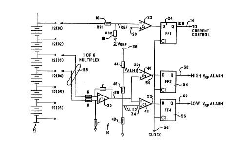
Turning first to Figure 1, a monitoring circuit 10 is shown, for monitoring
a series connected battery 12 while it is being charged.
United States Patent 5,179,33 and x,204,611, noted above, explain in detail
the operation of charging circuits where current control is derived from the
resistance free voltage of the battery being charged. For purposes of the
present
discussion, it is necessary merely to note that a current control output on
line 14
is derived from a resistance free voltage taken from the whole battery at
voltage
divider 16, 18, where the voltage thereby derived is compared by comparator 22
to an internally generated reference voltage presented at 20. The current
control
signal on line 14 is strobed by flip flop 24, under the control of a clock
pulse
presented at 26. In effect, the current control for the charger comes as a
consequence of the average resistance free battery voltage across the entire
battery
12.
However, each of the modules 12(01), 12(02), ... 12(06) is scanned in
keeping with the present invention to determine the resistance free voltage of
any
one of those modules individually, and thereby to detect and flag any module
which is abnormally low or abnormally high as to its resistance free
potential, in
the following manner:
A time division multiplexer is indicated at 28, whereby any one of the
modules 12(01) to 12(06) may be sampled at a time, with the sample being
applied
across the inputs of a differential amplifier ~0. Individual ampUtiers, one
across
each battery module, may of course be used. Two reference voltages 32 and 34
are derived as a function of the reference voltage at point 20, from point 36,
and
those two reference voltages at 32 and ~4 are compared to the output of
differential
S~PS:~~~~~~~ ~;-i~~
2121~'~1
9 (replacement)
amplifier 30 at 38, by comparators 40 and 42, respectively. The values of the
resistors in the string 44. -~6, 48, are chosen so that the reference voltages
at 32 and
34, and the outputs of the comparators 40 and 42 at 50 and 52, respectively,
may
be utilized to flag low or high resistance free voltages. In other words,
output 50
from comparator 40 is applied to flip flop 54; if the output 50 is high at the
time
of the positive transition of the strobe or clock pulse present at 26, it will
activate
an output on line 58 which will cause a high alarm. Likewise, if there is an
output
52 from the comparator 42, it will appear at line 60 through flip flop 56
strobed by
the clock pulse signal at ''6, to cause a low resistance free voltage alarm.
A typical time division multiplex scan of the resistance free voltage of
individual modules is shown in Figure 6. The resistance free voltage of the
selected module is present at the output 38 of amplifier 30 for a short
instant of
time when flip hops 54 and 56 are strobed by the clock signal at 26. The
resistance free voltage of each of the modules is shown in Figure 6 with
reference
to the voltage reference lines 62 and 64, which indicate the bounds of
acceptably
high module resistance free potential and acceptably low module resistance
free
potential, respectively. It will be noted that the output from module number
12(04), as shown in Figure 6, is unacceptably low:
The low resistance free voltage of any module will reveal that the module
contains a cell (or cells) which lacks the capability to hold charge due to
its poor
electrochemical activity; in other words, the module is either dead or dying.
Prematurely high resistance free voltage of a module during charging, on the
other
hand, indicates a module which contains a cell (or cells) having a lower and
presumably declining capacity to accept charge. That module will heat up more,
it will lose more water from its electrolyte (assuming an aqueous
electrolyte), and
it otherwise becomes a weak link in the battery 12. The circuit of Figure 1,
therefore, provides a diagnostic means whereby the weak link is identified,
and
therefore an early warning of impending trouble is given.
It is clear that the edge triggered flip flops 54 and 56 shown in Figure 1
could be substituted by other circuitry, such as sample and hold circuits as
identified in United States Patent 5,179,335, noted above.
21214'1
(replacement)
Moreover, it should be noted that the time division multiplex scan of Figure
6 may be representative of an output of a sample and hold amplifier which
samples
the resistance free module voltages as found at 84 of Figure 2, discussed
hereafter;
as well as the instantaneous output 38 of Figure 1, as discussed above.
~ typical utilization of a circuit in keeping with that of Figure 1 is its
adaptation to a monitoring circuit for a charger for a golf cart or an
industrial fork
lift truck and the like, having a 36 V lead acid battery which comprises six 6-
volt
modules.
Figure 2 provides a sampling and multiplexing circuit that is particularly
useful in circumstances where a high voltage battery is to be monitored,
during
both charge and discharge conditions. The battery 66, in the example chosen,
is
a 216 V battery, being comprised of 36 6-volt modules. They are indicated in
Figure 2. In this case, sensing wires are brought from the battery terminals
66+
and 66-, and from each of the intermodular nodes, as noted at wires 68-1, 68-
2, etc.
A solid state multiplexes 70 is provided, which may conveniently be one having
internal clamping diodes and an input common mode range of 0 to 1 ~ volts.
Operational amplifiers 72 and 74 are provided, and they translate the
individual
module voltages into a normalized single module voltage (or single cell
voltage)
v~e~~. That normalized single cell voltage is referenced to the negative
battery
terminal, in a time division multiplex. It is shown at terminal 76 as v~~,~
(t,N).
Two sample and hold circuits 78 and 80 are provided, from which two
further values are presented at terminals 82 and 84 as V~ and V~,
respectively.
The sample and hold circuits may conveniently comprise CBIOS bilateral
switches
~~78a and 80a, and holding capacitors 78b and 80b, as shown. The value V~ is
the
value of a cell or module voltage when the current is on -- that is. current
is
flowing through the battery -- and the value V~ is the resistance free voltage
that
is sensed for that same module or cell at a time that the current llow through
the
battery has been interrupted. In keeping with the teachings of the L;nited
States
Patents identified above, V~. may be the resistance free voltage of anv one of
the
modules as discussed hereafter during a time that the charging current to the
battery
has been interrupted under the control of the charger. ~s noted hereafter. V~
may
~~ ~y~
vw_~ ~~. ~,~ ~-
Y
2121~'~1
11 (replacement)
also be the resistance free voltage of a module where the current through the
module has been temporarily interrupted while the battery is under discharge
conditions.
Reference is made to Figure ~, for a discussion of representative wave forms
that may be found during operation of the circuit of Figure 2. Thus, a clock
wave
form is shown at curve 86. It may turn the charging current ON and OFF in
typical duty cycles having duty ratios in the range of 10:1 to 30:1. The
sample V~
and sample V~ signals are derived as "delayed ON" and "delayed OFF" signals
from the clock, so as to effect sampling of the V~ and V~ values during their
stable period -- after transients have died out as shown in curves 88 and 90.
Thus,
curve 92 shows sampling of curve 90 in a reasonably stable period with the
charging current off; and likewise curve 94 shows sampling of curve 90 in a
stable
period when charging current is flowing through the battery 66.
It should be noted that, during charge conditions, the voltage V~ is greater
than the V~,. value; however, during discharge conditions, the value of V~ is
less
than the V~.. Thus, the two conditions noted below should apply, and
conditions
other than those noted are abnormal:
V~ > VRF (during charge) Condition 1
V~ < VItF (during discharge) Condition 2
It will also be noted that a pair of terminals 96 and 98 are located within
the
battery 66. Those terminals are strategically located and are associated with
temperature sensors located within or applied to the battery 66, by which the
temperature condition of the battery may be continuously determined in a
manner
as discussed below.
There is also an address counter 100 with which is associated a suitable
display means 102. The address counter 100 and the module address display 102
work together so that. the identity of each module that is being sampled at
any
instant in time is displayed. The operation of the multiplexer 70 is such that
it has
a scanning rate of 1 or 2 Hz, which thereby allows the battery 66 having 36
modules to be scanned entirely in about 18 to 36 seconds. That scanning rate
is
sufficient that an observer may easily read the output on the module address
~~, ;:a>,;w _.. ; __
2121~'~1
22 (replacement)
display 102. so that if an alarm situation occurs the identity of the non-
conforming
module may be easily learned without the necessity for other associated
circuitry.
Of course, a higher scanning rate, in the order of about 10 Hz, will provide
for a
complete scan of the battery in 3.6 seconds; but in that case, the visual
presentation
on the module address display 102 might have to be stowed down such as by
latching the address counter value of the offending module in a latch inserted
between the counter 100 and the display 102.
The address counter 100 may be driven from its own clock, having an input
at 101. The address counter clock may be asynchronous with respect to the
internal clock within the battery charging circuits, having an input at line
118 as
noted below. More generally, however, the clock inputs at 101 and 118 are
synchronous. Thus, the clock input to the address counter 100 and 101 may
conveniently be a binary fraction of the clock input at line 118, for example
1/2,
1/4, 1/8 or 1/16. That means that the address counter 100 and time division
multiplexer 70 will dwell on any single module 66(01), 66(02), 66(n) etc., for
?,
4, 8 or 16 charging interruptions under the control of the internal clock.
Moreover,
the address counter clock at 101 may run at the same speed as the internal
clock,
for example at 10 Hz; but that puts extra demands on the sample and hold
circuits
78 and 80, since they must acquire and stabilize the correct values of V~ and
VRF
rather quickly.
It will be noted that terminals 76, 82, 84, 96 and 98 are found in each of
Figures 2 and 3. The circuit of Figure 3 includes charging current control
circuitry,
and analysis circuitry, by which the operation and control of the battery 66
may be
effected at least as to its charging operation, and by which the battery is
monitored
at all times during both charge and discharge operations.
The time dependent wave form v~e~~(t,N) appears at terminal 76, and in
keeping with the teachings of the above noted United States Patents with
respect
to battery charging circuits, it is applied at an input of comparator 104. The
other
input of comparator 104 is a voltage reference input at 106, and it comes as a
consequence of temperature compensation circuitry 108 in keeping with the
teachings of United States Patent ,?04,611, noted above. The temperature
~~; ,;-~r.:~";, .
2121411
"' 1'3'- 'f~placement)
compensation circuitry 108 also issues a further output at 110, which is an
input
to comparator 112 together with the same input from terminal 76. A pair of
flip
Hops 114 and 116 are each controlled by a clock signal from line 118, where
the
clock signal is from an internal clock within the battery charging circuits,
and is
adapted to strobe the operation of flip flops 114 and 116. The output of
comparator 104 appears at 120, and is an input to flip flop 114; likewise, the
output
from comparator 112 at 122 is an input to flip flop 116. w
The clock Line 118 also appears as an input to a digital potentiometer 124,
whose inputs include the output of flip flop 114 at line 126, and a time-out
input
signifying the expiration of a predetermined period of time T1 (as discussed
hereafter) at line 128. The output of the digital potentiometer is an analog
signal
which appears on line 130, and which is used to control the charging current
delivered to the battery 66.
In the usual manner, and in the absence of an alarm condition which may
occur as a consequence of the temperature of the battery 66 being beyond
predetermined limits, the control circuit comprising comparator 104, flip flop
114,
and digital potentiometer 124 is operative during charging conditions. When a
charging sequence is first initiated, a predetermined - period of time T l is
started,
and the digital potentiometer 124 is permitted to adjust its output at 130
both
upwards and downwards as a consequence of the input to it at line 126. Thus,
if
the battery 66 is substantially fully discharged, most if not all of the
modules
66(01) to 66(36) will request an up motion of the digital potentiometer by the
value
determined at terminal 76 and reflected at line 126, thereby forcing the
digital
potentiometer 124 to take its output at 130 upwards. The operation of the
digital
potentiometer 124 is essentially that of an averaging potentiometer, having
taken
an integration of the time dependent module voltages presented at terminal 76
during a scanning sequence by the multiplexer 70. On the other hand, if the
battery
76 is substantially fully charged, the same averaging function of the digital
potentiometer 124 will find a position which is such that the analog output at
line
130 is below its maximum value, being essentially that position where the
number
of modules requesting an "up" operation by the digital potentiometer 124 is
equal
,.. . . .
2I~1471
14 (replacement)
to the number of modules which requests a "down" operation. These sequences,
and the adjustment of the analog output at line 130, will continue for the
predetermined time period Tl, which is typically one minute.
When the time-out signal appears at line 128 at the end of time period TI,
the digital potentiometer 124 is then configured so that it can only move
downwardlv as to its analog output at line 130. A one way controller as
discussed
in United States Patent 5,204,61 l, identified above, then becomes effective.
Thus,
the analog current control output on line 130 will continue to move "down",
and
adjustments will continue to the charging current; and it is clear that the
downward
adjustments will be made according to the time dependent waveform V~e~l(t,~
whenever the V~ of any module reaches the reference voltage value, which is
indicative of that module (or cell) of the battery 66 which has the least or
lowest
charge acceptance capability. Thus, charging of the battery 66 will occur only
at
a rate at which the weakest or worst module or cell of the battery can accept
charge, so as not to abuse that module.
Of course, because of the operation of the analog counter 100 and the
module address display 102, the identity of the module which is requesting the
downward operation of the digital potentiometer 124 can be easily determined.
The operation of comparator 112 and flip flop 116 is such that if a module
in battery 66 has been so severely overdischarged or has failed, to the extent
that
a reference voltage for that module or cell is below a predetermined limit, an
immediate signal will occur such as at the LED 132 in coincidence with the
identity of that failed module or cell, which will appear at the display 102.
When the battery 66 is being discharged, the output of the circuit
comprising the temperature compensating circuitry 108, comparator 112, and
flip
flop 116, can be used to indicate a circumstance within the battery 66 which
is
analogous to a "LOW FUEL" circumstance in an ordinary automobile. In that
case,
the discharge current permitted to flow through the battery 66 may be limited
to
a progressively lower value. Ultimately, a situation may occur when the
weakest
module or cell in the battery 66 is not able to sustain a circumstance where
its
resistance free voltage at a predetermined value of discharge current is not
higher
~, j .; =.r ::':
2121471
15 (replacement)
than a predetermined cut off voltage, and at that point the analogy continues
such
that the battery 66 is essentially "EMPTY", and further discharge of the
battery 66
is inhibited.
It will be noted that terminals 82 and 84 which, respectively, carry a signal
indicative of the value of a module or cell voltage through any specific
module
when current is flowing through the battery 66 as determined at the sample and
hold circuit 78, and the resistance free value of the module or cell when the
current
is not flowing through the battery 66 as determined at sample and hold circuit
80,
are the two inputs to amplifier 134. Its output appears at line 136, and is
one of
the two inputs to each of comparators 138 and 140. The other input to
comparators
138 and 140 comes from line 142, and is defined as the predetermined value of
the
resistive voltage drop, BVR. The input to comparator 138, however, is inverted
through an inverting amplifier 139, so as to be of the opposite sense to the
aVR
input to comparator 140. The defined value aV is the resistive drop through
the
module being sampled at any time while current is flowing -- in other words,
the
voltage across the module which is the product of the current through the
module
and its internal resistance.
An OR gate 144 is adapted to take the outputs from each of comparators
13 8 and 140 on lines 146 and 148, respectively.
It will be noted that comparators 138 and 140 have their inputs from lines
136 and 142 reversed with respect to each other. Moreover, as noted above, the
aVR input to comparator 138 is inverted to the sense of the same input to
comparator 140. Thus, the output of comparator 138 occurs during a charging
operation when the module voltage V~ at terminal 82 is greater than the
resistance
free voltage V~ at terminal 84, and its difference is greater than SV~.
Likewise,
the output at line 148 from comparator 140 occurs when the difference between
V~ and V~ is greater than 8VR at any time while the battery 66 is being
discharged.
It follows that the output from the OR gate 144 at line 1~0 will illuminate
the LED 152 when the absolute value of the difference between V~ and V~. is
greater than BVR, which is expressed as follows:
~~~~ i~i~'~T~ 5~~~
~121~~~
16 (replacement)
Vc - VRF ~ ~ aVR Condition 3
It will also be noted that the lamp 1 ~2 will remain illuminated in
coincidence with the module address display 102, whereby the identity of the
module will be noted. From this, it can be determined that a specific module
or
cell has a high resistive drop across it as current flows through it, and
therefore that
it has a high resistance.
Obviously, it is most important to monitor the condition of LED 1~2 during
any period when current through the batter v 66 is at its maximum, because at
that
time the resistive drop aV and the dissipated resistance heat from any high
resistance module will be at their highest level, as follows where Qmodule is
the
dissipated resistive heat:
Vc - VRF ~ - Rmoduie Y I
Qmoduie - sV ~ I - "module ~ IZ
It should also be noted that connecting leads or bridges between the battery
cells or modules may also contribute some resistance due to their own wire
resistance as well as any contact resistance R~; so that the module resistance
~,odu~e will be the sum of the internal resistance R;nc of the module plus R~.
Therefore, monitoring the condition of LED 152 and the address of any
module indicated on the module address display 102 will not only indicate a
faulty
module or cell, it will also indicate the existence of a faulty intermodular~
connection or contact, such as a loose or corroded contact. Indeed,
experimental
testing of circuits according to the present invention. more specifically in
keeping
with the circuit of Figure l, resulted in a damaged battery terminal which
came as
a consequence of a loose contact. If the monitoring circuits of Figures 2 and
3 had
been in operation, that loose contact would have been immediately noted and
diagnosed,. before any wotable damage could have occurred.
Figure 4 illustrates a typical time division multiplex scan of the output of
differential amplifier 134 at line 136. In This Figure, the identity of each
module
is noted as indicated at 1 ~4, and the scanning curve I ~6 is compared against
a
predetermined 8VR value shown at 1~8. It will be noted that 8V for module
13
2121~'~1
17 (replacement)
66(00 exceeds the predetermined value, and thus an alarm condition will occur
such that LED 1~2 will be illuminated in coincidence with the address (OS)
being
displayed at the module address display 102. The 8V value for module 66(08) is
also higher than average, but remains below the alarm threshold so that an
alarm
condition would not occur as a consequence of the aV value for that module
66(08).
Turning to Figure 7, a scheme is shown to incorporate a simple and
inexpensive single chip microcomputer 160 with the time division multiplex
scanning as shown in Figure 2. Thus, terminals 76, 82, and 84 are found in
Figure
7, carrying the same values as in each of Figures 2 and 3, and a further
terminal
162 is also found on which appears a signal indicative of the value of the
current
IB flowing through the battery 66. Each of those inputs is to an analog-to-
digital
converter 164, which interacts with the microcomputer 160. An input/output
interface 166 is interposed between the microcomputer 160 and the multiplexes
70;
and it also provides means for sending alarm signals from the microcomputer
160
to such devices as a visual alarm 168 and an audio alarm 170. A display 172
may
optionally also be associated with the microcomputer 160, to display the
address
of any module being sampled in the same manner as the module address display
102 in Figures 2 and 3. The display 172 may optionally be arranged to display
other diagnostic data or messages concerning the status of the battery, such
as its
temperature, its state of charge, and the like.
Obviously, by use of the microcomputer 160, very sophisticated monitoring
can be undertaken, from which sophisticated information processing and
evaluation
as to the performance and diagnostics concerning the condition of the battery
66
may be made. A scanning speed for the multiplexes 70 can be increased, for
example to 10 Hz, whereby the 36 module battery 66 can be scanned in 3.6
seconds. Moreover, computations may be performed whereby each of the module
or cell resistances is monitored at all times. As well, mean values and mean
deviations of key parameters such as the values of V~ at terminal 82 and VRp
at
terminal 84 with respect to the battery current IB at terminal 162, will
derive an
instantaneous value for the module resistance as a function of the absolute
value
21214'~I
18 (replacement)
of V~ minus the absolute value of V~. divided by the absolute value of the
battery
current IB, as follows:
~ _ uc ' VRF
"module -
IB
Still further, it is possible to improve heat management of the heat
dissipated within the battery 66, because the resistive heat dissipated comes
as a
consequence of the instantaneous value of the battery current, as follows:
Qmodule - ~odule Y IBZ
That means that the resistive heat dissipated in each individual battery
module or cell can be individually monitored, which provides an improvement
over
the use of temperature sensors having outputs only at terminals 96 and 98 as
indicated in Figure 2.
Still further, monitoring the resistance free voltage of individual modules
provides yet a further refined means whereby the state of charge of the
battery can
be determined. In other words, and to conclude the analogy to an ordinary
automobile, a better "fuel gauge" is provided by the use of circuits such as
that
indicated in Figure 7.
There has been described the importance of monitoring two important
parameters of a large scale battery, both under charge and under discharge
conditions. They are., of course, the electrochemical potential -- the
resistance free
voltage -- of the individual modules of the battery, and the resistive drop
across
each of the individual modules in a series connected battery as charging or
discharge current flows through the battery. Clearly it is open to monitor and
interpret as many levels of voltage drop, current, voltage differentials, and
so on,
as the sophistication and capital cost of the circuits may permit and as may
be
required in any given circumstance. Thus, the specific computations that may
be
made, the warnings and alarms that are generated, and the results thereby
conveyed
to the operator or driver of an electric vehicle, are notsimply or
specifically
restricted to those described above. However, the discussions above indicate
the
manner in which circuits according to the present invention may be utilized
for
such purposes. '
~. ~~ :w f ~ , ..
2121 ~'~1
19 (replacement)
Finally, it has been noted that by monitoring the resistance free voltage of
a module and the resistive drop across the module during discharge -- for
example,
during the operation of an electric vehicle -- important information
concerning the
state of charge of the battery is determined. Thus, the circuits provide means
by
which overdischarge of a battery may be precluded, thereby preventing serious
damage to the battery. The number of modules present in the battery is not
material to the present invention, and the discussions above are merely
illustrative
of the principles of the invention and not limiting thereto.
Obviously, even during discharge there must be short interruptions of that
discharge current, in order that the resistance free voltage across any module
may
be deternined. Thus, circuits in keeping with the present invention would be
designed to integzate and work closely with the traction controller of an
electric
vehicle powered by a large scale battery, so that instantaneous interruptions
of the
discharge current flowing from a battery may occur under conditions where the
operation of the vehicle is not affected. Since electric vehicles that are
presently
being tested, and electric vehicles as foreseen in the future, all have solid
state
controllers, there is no reason or concern that such monitoring cannot be
effectively
carried out. Still further, it can be noted that by monitoring the resistance
free
voltage of the battery modules, potentially damaging overcharge to the battery
can
be precluded during such vehicle operations as regenerative braking.
The scope of the present invention is defined by the appended claims.
.._ ,. _ .: ~N.'-'
. ..