Note: Descriptions are shown in the official language in which they were submitted.
7 B ~
FIELD OF THE INVENTION AND RELATED ART
The present invention relates to a liquid
crystal device which may be used as a display device
for a television receiver, a view finder for a video
camera or a terminal monitor for a computer, or a
light valve (optical shutter) for a liquid crystal
printer, a projector, etc.
A liquid crystal display device of a passive
matrix drive-type using a TN (twisted nematic) liquid
crystal has been known as a device which can be
produced at a relatively low cost. The passive
matrix-drive type liquid crystal device using a TN-
liquid crystal has a certain limitation due to the
occurrence of a crosstalk or a lowering in contrast
along with the increase in number of drive lines so
that it cannot be said to be suitable as a display
device requiring a high resolution and a large number
of drive lines, e.g., a liquid crystal television
panel.
As a type of liquid crystal device having
solved such a fundamental problem of a conventional
TN-liquid crystal device, there has been known a
ferroelectric liquid crystal device having
bistability. In the ferroelectric liquid crystal
device, a liquid crystal showin~ a chiral smectic
~ 13
2121776
-2-
phase, such as chiral smectic C (SmC*) phase or chiral
smectic H (SmH*) phase, in its operational state is
used. The liquid crystal tends to assume one of two
bistable states and does not readily assume an
intermediate molecular position. Further, this type
of liquid crystal quickly assumes one of the two
stable states in response to an electric field applied
thereto and retains the resultant state in the absence
of an electric field. By utilizing a chiral smectic
liquid crystal showing such properties to constitute a
liquid crystal device, it has become possible to
provide substantial improvements to the problems of a
conventional TN-liquid crystal device, inclusive of a
poor viewing angle characteristic.
In this type of chiral smectic liquid crystal
device, however, there has been found a problem that
liquid crystal molecules can move in a direction
parallel to the substrate extension in some cases
under application of an electric field. As a result
of the movement, there is caused a phenomenon that the
cell thickness (spacing between a pair of substrates
sandwiching a liquid crystal material) is changed to
provide a pale yellow tint on a display picture (which
phenomenon may be referred to as "yellowing"). The
phenomenon is not desirable not only for a display
device but also for any other optical modulation
device as it causes a deterioration in optical
_3_ ~ ~ 2~
performance.
In order to suppress such a liquid crystal
molecular movement, there has been proposed a
technique of roughening the inner surface of a
substrate in EP-A 0550846.
The above-mentioned inner surface roughening
technique has not been always satisfactory. This is
because the inner surface roughening as a technique of
physically or dynamically suppressing the liquid
crystal molecular movement is not always preferred,
since, for example, some liquid crystal can provide a
better alignment quality if the inner surface is free
from roughening.
Further, while the surface roughening is
effective for suppressing the yellowing on a display
of an ordinary display as used in character
compilation, the yellowing can be still liable to be
caused on a display of a certain special graphic
display pattern.
SUMMARY OF THE INVENTION
In view of the above-mentioned problems of
the prior art, an object of the present invention is
to provide a liquid crystal device having a simple
structure, in which a cell thickness change hardly
~,
2121 776
-4-
occurs, and also an apparatus using the liquid crystal
device.
Another object of the present invention is to
provide a liquid crystal device wherein a substantial
cell thickness change hardly occurs even if a liquid
crystal molecular movement occurs, and also an
apparatus using the liquid crystal device.
Another object of the present invention is to
provide a liquid crystal device excellent in wide
applicability, wherein a cell thickness change hardly
occurs even if any liquid crystal material is used
therein and any drive method is applied thereto, and
also an apparatus using the liquid crystal device.
A further object of the present invention is
to provide a liquid crystal device with excellent
reliability and free from deterioration in optical
characteristic.
According to an aspect of the present
invention, there is provided a liquid crystal device
comprising a pair of oppositely disposed substrates
having opposing inner surfaces and opposing electrodes
thereon, and a chiral smectic liquid crystal disposed
between the opposing electrodes, said liquid crystal
device having an effective optical modulation region
and a peripheral region outside the effective optical
modulation region; wherein liquid crystal molecules in
the peripheral region have a pretilt angle which is
2 12177~
larger than a pretilt angle of liquid crystal
molecules in the effective optical modulation region.
The following features may preferably be
added by selection in order to enhance the effect of
the present invention. Thus, it is preferred to
roughen the inner surface of at least one of the pair
of substrates.
It is also preferred that the liquid crystal
molecules in the effective optical modulation region
have a high pretilt angle of at least lO degrees or a
low pretilt angle of at least 5 degrees.
It is preferred that the peripheral region is
divided into a first region adjacent to the effective
optical modulation region and a second region outside
the first region, so that the liquid crystal molecules
in the first region have a pretilt angle substantially
equal to that in the effective optical modulation
region, and the liquid crystal molecules in the second
region have a pretilt angle larger than that in the
effective optical modulation region.
It is preferred that a plurality of adhesive
particles and a plurality of spacers are disposed
between the substrates.
It is also preferred that the opposing
electrodes are supplied with a drive signal comprising
bipolar pulses, with respect to a reference potential,
for driving.
2121 77~
-6-
It is also preferred that the peripheral
region is optically covered with a masking member.
As a result of our study, it has been found
that the density irregularity of liquid crystal
molecules leading to a cell thickness change in the
effective optical modulation region can be relaxed by
placing the liquid crystal molecules in the peripheral
region outside the effective optical modulation region
in a high pretilt state so as to increase the mobility
of the liquid crystal molecules in the peripheral
region. It has been also found possible to cause some
liquid crystal molecules to move from the peripheral
region to a low-density portion.
In this way, in contrast to a conventional
technique of only intending to suppress the liquid
crystal molecular movement, it is intended to
positively utilize the movement of liquid crystal
molecules to prevent a cell thickness change, thus
preventing the occurrence of yellowing, in the present
invention.
As a result, according to the present
invention, the yellowing due to a cell thickness
change hardly occurs, even if the liquid crystal
material or a drive scheme which has been liable to
cause a cell thickness change is used or even if a
display pattern which has been liable to cause a cell
thickness change is displayed.
212177~.~
-7-
These and other objects, features and
advantages of the present invention will become more
apparent upon a consideration of the following
description of the preferred embodiments of the
present invention taken in conjunction with the
accompanying drawings.
BRIEF DESCRIPTION OF THE DRAWINGS
Figure lA is a schematic plan view of a
preferred embodiment of the liquid crystal device
according to the invention, and Figure lB is a
schematic sectional view taken along a line A-A' in
Figure lA.
Figures 2A and 2B are explanatory views for
illustrating a liquid crystal molecular movement in a
liquid crystal device.
Figures 3A and 3B are explanatory views for
illustrating a liquid crystal molecular movement in an
embodiment of the liquid crystal device according to
the invention.
Figure 4 is an explanatory view for
illustrating an alignment state occurring in a chiral
smectic liquid crystal used in the invention.
Figures 5A and 5B are explanatory views for
illustrating changes in director orientation according
to various positions between substrates in Cl
alignment and C2 alignment, respectively, in a chevron
212177~
structure of a smectic liquid crystal.
Figures 6A and 6B are schematic illustration
of a bookshelf structure of a smectic liquid crystal.
Figures 7A and 7B are schematic illustrations
of a rubbing method.
Figure 8 is a block diagram of an image
display apparatus including a liquid crystal device
according to the invention.
Figure 9 is a schematic illustration of an
image forming apparatus including a liquid crystal
device according to the invention.
Figure lOA is a waveform diagram illustrating
a set of drive signals for driving a liquid crystal
device accordingto the invention, and Figure lOB is an
illustration of the resultant display state.
Figures 11 and 12 are a schematic plan view
and a schematic sectional view, respectively of a
first embodiment of the liquid crystal device
according to the invention.
Figures 13 - 15 are schematic plan views of
second to fourth embodiments, respectively, of the
liquid crystal device according to the invention.
Figure 16 is a schematic plan view for
illustrating a manner of evaluating liquid crystal
molecular movement.
2121 77~
-9-
DESCRIPTION OF THE PREFERRED EMBODIMENTS
The liquid crystal device according to the
present invention is basically applicable to any type
of optical modulation but may preferably be applied to
a type of optical modulation as used in an optical
shutter or a light valve capable of controlling the
light transmittance through each pixel at binary
levels or multiple levels. The pixel addressing
scheme may be one of a multiplex scheme using an
electrode matrix or a photo-address scheme using a
photoconductor film.
Figure lA is a schematic plan view of a
preferred embodiment of the liquid crystal device
according to the present invention, and Figure lB is a
schematic sectional view taken along an A-A' line as
view in the direction of arrows in Figure lA.
Referring to Figure lA, a liquid crystal
device (cell or panel) 1 schematically has a planar
shape as shown, including an effective optical
modulation region 2, a peripheral region 3 adjacent to
and outside the region 2, and a sealing part 4
surrounding the peripheral region 3 except for an
injection port 5, which is sealed with a sealing
member after the liquid crystal injection.
Referring to Figure lB, the liquid crystal
device includes a pair of an upper substrate lla and a
lower substrate llb, each having electrodes (not
2121776
-10-
shown) thereon. The substrates lla and llb are
provided with peripheral alignment control regions 13a
and 13b, respectively, for providing a high pretilt
angle a2 to the liquid crystal in the peripheral
region 3, and alignment control regions 14a and 14b,
respectively, for providing a low pretilt angle al to
the liquid crystal in the effective optical modulation
region, satisfying a1 < a2. Between the substrates
lla and llb is disposed a liquid crystal material 15
which is capable of showing a chiral smectic phase and
can cause liquid crystal molecular movement when
driven under application of an electric field in a
conventional liquid crystal cell structure.
Herein, the effective optical modulation
region refers to a display region including a large
number of pixels to effect a display by controlling
the transmittance through the respective pixels in the
case of a display device, and to a region of effecting
optical modulation depending on drive signals in the
case of a non-display device, such as a light valve.
According to our study, the increase in cell
thickness is recognized to be caused by a pressure
increase, which in turn is caused by movement of
liquid crystal molecules in a particular direction due
to driving, particularly at a cell side. Presumably,
such a force causing the liquid crystal molecule
movement may be attributable to an electrodynamic
2 11 2 ~ 6
effect caused by perturbation of liquid crystal
molecule dipole moments in an AC-like electric field
caused by continuation of drive pulses. Further,
according to our experiments, the directions 22a and
22b of the liquid crystal movement are determined in
relation with the rubbing direction 20 and the average
liquid crystal molecular axis position 21a or 21b as
shown in Figure 2A. As the moving direction of liquid
crystal molecules is related with the rubbing
direction, the above-mentioned phenomenon is assumed
to depend on the pre-tilt state at the substrate
surfaces. Referring to Figures 2A and 2B, reference
numeral 21a (or 21b in a reverse orientation state)
denotes an average molecular axis (director)
orientation. When the liquid crystal molecules
(described herein as having a negative spontaneous
polarization) are oriented to provide the average
molecular axis 21a and are supplied with a certain
strength of AC electric field not causing a switching
to the orientation state 2lb, the liquid crystal
molecules are liable to move in the direction of an
arrow 22a in the case where the substrates are
provided with rubbing axes extending in parallel and
in the same direction 20. This liquid crystal
movement phenomenon depends on an alignment state in
the cell.
In an actual liquid crystal cell, the liquid
-12- ~ 77~ '
crystal movement occurs as shown in Figure 2A. For
example, when the liquid crystal molecules in the
entire cell are placed in a state providing an average
molecular axis direction 21a, the liquid crystal
molecules in the cell are liable to move under AC
application in the direction of the arrow 22a, i.e.,
from the right to the left in the figure. As a
result, the cell thickness in a region 23 is increased
gradually to show a yellowish tint. If the liquid
crystal molecules are placed in a state providing an
average molecular axis 21b, the liquid crystal
movement under AC application is caused in the reverse
direction 22b. In either case, the liquid crystal
movement is liable to be caused in a direction
perpendicular to the rubbing direction, i.e., in the
direction of extension of smectic layers. It has been
also observed that a cell thickness increase is also
caused in a direction of a normal to smectic layers in
addition to the direction of smectic layers as
mentioned above.
According to another experiment, when a black
(BL)-and-white (W) stripe pattern is continually
displayed on a display panel formed by rubbing in a
direction R as shown in Figure 3A, liquid crystal
molecules in a region of displaying "black" (BL or
dark) placed in an average molecular axis direction
2la are moved in the direction of an arrow _ to
. .~
2 1~:17~1~
-13-
provide a panel side region A which shows a larger
cell thickness than the surrounding region. On the
other hand, liquid crystal molecules placed in an
average molecular axis direction 21b in a region of
displaying "white" (W or bright) are moved in the
direction of an arrow b to provide a panel side region
B having an increased cell thickness on the opposite
side.
In contrast thereto, it has been found that,
in case where a peripheral region 3 is disposed to
surround a display region 2 (as an effective optical
modulation region) and a high pretilt alignment state
is established in the peripheral region, the liquid
crystal molecules in the black-displaying state moving
in the direction a can further move to the peripheral
region 3 and the liquid crystal molecules collected in
the peripheral region can further move in directions c
and d. Reversely, liquid crystal molecules can also
move in a direction e.
On the other hand, in the white-display
region, accompanying the liquid crystal movement in
the direction b, liquid crystal molecules collected in
the peripheral region can move in directions cc and dd
and also in a direction ee.
The above phenomenon is caused presumably
because as liquid crystal molecules are aligned with a
higher pretilt angle, i.e., closed to a homeotropic
2 12177~
-14-
alignment, smectic layers formed along panel surfaces
approach an isotropic state, so that liquid crystal
molecules are caused to move in an isotropic manner in
response to an external electric field applied
thereto.
As a result, in a liquid crystal panel
according to the present invention, even if a pressure
distribution is developed as a result of liquid
crystal molecular movement as shown in Figure 3A, the
pressure distribution is relaxed by the isotropic
movement of liquid crystal molecules in the peripheral
region as shown in Figure 3B, thereby suppressing the
cell thickness increase along a panel side.
While Figure 3B shows a most preferred
embodiment wherein the peripheral region is disposed
along the entire periphery of a panel, this is not
essential, so that the peripheral region can be
disposed, e.g., only the upper and lower sides of the
panel shown in Figure 3B.
In further preferred embodiments, the
following features may preferably be adopted by
selection.
It is preferred that at least one of the
substrates constituting the liquid crystal device
according to the present invention is roughened with
respect to the inner surface thereof. This is
because, if the liquid crystal molecular movement in
2121776
the effective optical modulation region is suppressed
to some extent by a roughened inner surface, it is
possible to optimize the liquid crystal injection from
the peripheral region and the release of the liquid
crystal to the peripheral region in good balance with
the movement in the effective optical modulation
region. The roughened surface prepared for this
purpose may be either a regular or an irregular one.
There are two effective design concepts
1~ regarding the pretilt angle in the effective optical
modulation region. According to one thereof, an
aligning treatment is effected so as to provide a
pretilt angle in the range of lO - 25 degrees.
According to the other one, the pretilt angle is
suppressed to at most 5 degrees. The former design is
effective for readily providing a chevron structure
wherein smectic layers are bent between the
substrates, e.g., by providing axes of uniaxial
alignment as by rubbing or oblique evaporation which
are in mutually parallel and substantially identical
directions to a pair of substrates constituting the
liquid crystal device. A resultant high-pretilt
chevron structure is advantageous in that an alignment
disorder is not readily caused even in contact with a
roughened inner surface. The latter design is
effective for readily providing a bookshelf structure
wherein smectic layers are free from bending between
2 1 ~ 1 7 7 ~
-16-
the substrates, e.g., by providing uniaxial alignment
aces which are in mutually parallel and opposite
directions to a pair of substrates or by providing a
uniaxial alignment axis to only one of a pair of
substrates. In a resultant low-pretilt bookshelf
structure, the liquid crystal molecular movement
velocity is relatively small even without roughening
of the inner surfaces, so that a good balance with the
moving speed to and from the peripheral region can be
easily accomplished. The low-pretilt bookshelf
structure may provide a better alignment state in
respect of optical characteristic.
The peripheral region according to the
present invention need not be disposed so as to
lS surround the entirety of the effective optical
modulation region. It is sufficient to dispose such a
peripheral region on both lateral sides or on both
longitudinal sides, preferably in a direction of
smectic layer extension. The peripheral region may
preferably have a width which is larger than that of
one pixel. It is preferred to optically mask the
peripheral region by a masking member or a light-
interrupting member so as to substantially not
effecting an optical modulation. It is theoretically
sufficient that the peripheral region has a large
pretilt angle than that in the effective optical
modulation region even if the difference is small
2 1 2 1 7 7 ~
-17-
since a larger mobility can be realized in the
peripheral region than in the effective optical
modulation region. Actually, however, it is preferred
to have a difference in pretilt angle of at least lO
degrees. In order to facilitate the cell production,
a substantially homeotropic alignment is desirable.
The peripheral region can partially include a
sub-region wherein the pretilt angle is similar to
that in the effective optical modulation region. The
sub-region may preferably be disposed adjacent to the
effective optical modulation region.
It is possible to dispose electrodes in the
peripheral region similarly as in the effective
optical modulation region so as to promote the liquid
crystal molecular movement by selectively applying an
electric field. The electric field may preferably be
given by drive signals identical to those of scanning
signals and/or data signals for driving the liquid
crystal at the pixels in the effective optical
modulation region.
In the preparation of a cell, it is preferred
to disperse spacer beads and adhesive beads between
the substrates so as to suppress the liquid crystal
molecular movement in the effective optical modulation
region
Next, microscopic structures of a smectic
liquid crystal used in the present invention will be
212177~
-18-
described.
The alignment state in smectic phase
including a chevron structure may be described as
including two alignment states of C1 and C2 as shown
in Figure 4. Referring to Figure 4, reference numeral
31 denotes a smectic layer, 32 denotes a C1 alignment
region, and 33 denotes a C2 alignment region. A
smectic liquid crystal generally has a layer structure
and causes a shrinkage of layer pitch when it is
transformed from SmA (smectic A) phase into SmC
(smectic C) phase or SmC* (chiral smectic C) phase, to
result in a structure accompanied with a bending of
layers between the upper and lower substrates 14a and
14b (chevron structure) as shown in Figure 4. The
bending of the layers 31 can be caused in two ways
corresponding to the C1 and C2 alignment as shown. As
is well known, liquid crystal molecules at the
substrate surfaces are aligned to form a certain angle
a (pre-tilt) as a result of rubbing in a direction A
in such a manner that their heads (leading ends) in
the rubbing direction are up (or away) from the
substrate surfaces lla and llb. Because of the pre-
tilt, the C1 and C2 alignment states are not
equivalent to each other with respect to their elastic
energy, and a transition between these states can be
caused at a certain temperature or when supplied with
a mechanical stress. When the layer structure shown
212177~
- 1 9 -
in Figure 4 is viewed in plan as shown in the upper
part of Figure 4, a boundary 34 of transition from C1
alignment (32) to C2 alignment (33) in the rubbing
direction A looks like a zigzag lightning and is
called a lightning defect, and a boundary 35 of
transition from C2 alignment (33) to Cl alignment (32)
forms a broad and moderate curve and is called a
hairpin defect.
When a chiral smectic liquid crystal is
disposed between a pair of substrates lla and llb
provided with uniaxial alignment axes which are
substantially parallel to each other and identical in
direction as by a uniaxial aligning treatment, such as
rubbing, and the liquid crystal is placed in an
alignment state satisfying a relationship of ~ < a +
...(1), wherein a denotes a pretilt angle of the
liquid crystal, ~ denotes a tilt angle (a half of
cone angle), and ~ denotes an angle of inclination of
SmC* layer, there are four states each having a
chevron structure in the C1 alignment state. These
four C1 alignment states are different from the known
Cl alignment state. Further, two among the four Cl
alignment states form bistable states (uniform
alignment). Herein, two states among the four C1
states giving an apparent tilt angle ~a therebetween
in the absence of an electric field satisfying a
relationship of ~ >-~a > ~ /2 ...(2) are inclusively
2 ~ ~ 77~ ~
-20-
referred to as a uniform state.
In the uniform state, the directors are
believed to be not twisted between the substrates in
view of optical properties thereof. Figure 5A is a
schematic view illustrating director positions between
the substrates in the respective-states in C1
alignment. More specifically, at 51 - 54 are
respectively shown changes in director positions
between the substrates in the form of projections of
directors onto cone bottoms as viewed from each
bottom. At 51 and 52 is shown a splay state, and at
53 and 54-is shown a director arrangement which is
believed to represent a uniform alignment state. As
is understood from Figure 5A, at 53 and 54
representing a uniform state, the molecule position
(director) is different from that in the splay state
either at the upper substrate or lower substrate.
Figure 5B shows two states 55 and 56 in C2 alignment between
which no switching is observed at the boundaries but
an internal switching is observed. The uniform states
53 and 54 in C1 alignment provide a larger tilt angle
~a and thus a higher brightness and a higher contrast
than the conventionally used bistable state in C2
alignment.
In contrast thereto, Figures 6A and 6B
schematically show smectic layer structures of a
bookshelf structure, including an oblique bookshelf
22~2177~
structure of a low pretilt angle (~1) shown in Figure
6A and an oblique bookshelf structure of a high
pretilt angle (a2 > al) shown in Figure 6B.
In the present invention, it is preferred to
use a high-pretilt shevron structure in Cl alignment
having a pretilt angle of at least 10 degrees, more
preferably 10 - 25 degrees, or a low-pretilt bookshelf
structure having a pretilt angle of at most 10-
degrees, more preferably at most 5 degrees.
[Cell Structure]
The liquid crystal cell (device) according to
the present invention may be composed of a pair of
substrates which may be of any materials as far as at
least one thereof is transparent. Examples of the
transparent substrate material may include glass,
quartz and plastic sheets. On the other hand, a
substrate not requiring optical transparency can be of
any materials inclusive of metals, semiconductors and
insulating materials as far as it provides an
2~ appropriate substrate surface.
At least one of the opposing electrodes
respectively formed on the pair of substrates may
desirably be composed of a transparent conductor,
suitable examples of which may include: tin oxide,
indium oxide and indium tin oxide (ITO). According to
necessity, a transparent electrode may be supplemented
with a low-resistivity metal electrode disposed along
212177~
-22-
a side thereof. The electrode may preferably have a
thickness of 40 - 200 nm.
The substrates may be coated with an
alignment film, examples of which may include: films
of organic materials, such as polyimide, polypyrrole,
polyvinyl alcohol, polyamideimide, polyesterimide,
polyparaxylylene, polyester, polycarbonate, polyvinyl
acetal, polyvinyl chloride, polyamide, polystyrene,
polyaniline, cellulosic resin, acrylic resin and
melamine resin; and inorganic films, such as obliquely
evaporated film of SiO. The alignment film may
preferably have a thickness on the order of 5 - 100
nm. A desired pretilt angle may be provided by an
appropriate combination of a liquid crystal material
and an alignment film, but it is preferred to obtain a
desired pretilt angle by appropriately selecting the
degree of rubbing (e.g., rubbing intensity, number of
rubbing treatments, etc.).
In the present invention, it is also possible
to dispose an insulating film below the alignment
film. The insulating film may preferably comprise an
inorganic material such as TixSiyOz (x+y+z = 1), SiO2,
TiO or Ta2O5. In case of roughening the inner surface
of a substrate, it is preferred to disperse fine
particles of, e.g. oxides, such as SiO2, Al2O3, etc.,
in the insulating film.
An insulating film for providing a roughened
21'2177~
-23-
inner surface may for example be prepared by applying
a solution or dispersion of an inorganic film
precursor (e.g., one containing Ti and Si in a ratio
of l:lO - lO:l, preferably around 1:1) containing fine
particles dispersed therein on a substrate, followed
by baking. The degree of unevenness may be controlled
by changing the dispersion density and the average
particle size of the fine particles and the thickness
of the insulating film covering the fine particles.
The fine particles for providing a roughened inner
surface may preferably have a particle size of about 1
- lOO nm. The insulating film retaining the fine
particles therein may preferably have a thickness of
about 20 - 30 nm.
A high-pretilt alignment, preferably a
homeotropic alignment, may be formed in the peripheral
region by disposing on the substrate in the region
either one or both of the insulating film and the
alignment film, but not subjecting these films to
uniaxial aligning treatment such as rubbing.
The direction of the uniaxial alignment axis
as by rubbing may be disposed so that both sides in a
direction intersecting the alignment axis are provided
with the peripheral regions, whereby liquid crystal
molecules moved in a smectic layer reach one of the
high-pretilt peripheral regions which are disposed on
both ends of the smectic layer.
2~17~
-24-
(Preparation of liquid crystal cell)
A liquid crystal cell may for example be
prepared in the following manner.
A pair of transparent substrates of, e.g.,
glass, may be provided. Each substrate is provided
with a transparent conductor film by vapor deposition,
such as CVD (chemical vapor deposition), sputtering,
or ion plating, followed by patterning the conductor
film into stripes through, e.g., photolithographic
steps. The stripe electrodes may then be coated with
an insulating film as by vapor deposition. For
providing a roughened inner surface, an inorganic film
precursor solution containing fine particles dispersed
therein may be applied thereon, calcined and backed to
form an insulating film providing a rough surface.
Then, an alignment film may be formed, e.g., by
application of a polyamide acid solution by spinner
coating, followed by baking. The alignment film is
then subjected to a rubbing treatment. On the
substrate thus treated, spacer beads are dispersed and
a peripheral sealing member is applied except for a
part giving an injection port, and another substrate
similarly treated is applied thereon together with
additional dispersion of adhesive beads, if desired,
to form a blank cell. The blank cell is then
gradually filled with a liquid crystal material heated
to a higher temperature phase and injected through an
-25-
injection port and gradually cooled to cause a
transition to chiral smectic phase.
The display region and the peripheral region
providing different pretilt angles may be formed by
forming a homeotropic alignment film onto an entire
inner surface of a substrate and then selectively
rubbing a part of the substrate giving the display
region while masking a remaining part of the substrate
giving the peripheral region, or by disposing a low-
pretilt alignment film causing a low pretilt angle anda high-pretilt alignment film causing a high pretilt
angle at the display region and the peripheral region,
respectively, of the substrate.
In addition to the above-described method of
applying an insulating film-precursor solution
containing fine particles dispersed therein, the
roughening of a substrate inner surface may be
suitably performed by methods disclosed in EP-A
0550846.
Next, a preferred mode of rubbing will be
described.
Figures 7A and 7B are a perspective view and
a side view, respectively, schematically illustrating
a manner of rubbing treatment. Referring to these
figures, a rubbing apparatus (not entirely shown)
includes a rubbing roller 120 which comprises a
cylindrical roller 121 and a rubbing cloth 120, such
2l2177 ~
as nylon yarn-planted cloth, wound about the roller
121. The rubbing roller 120 is rotated in a direction
C and simultaneously caused to contact an alignment
film 14a (or 14b) on a substrate lla (or llb) at a
prescribed pressure while moving the glass substrate
lla (or llb) in a direction B or moving the roller 120
in a counterdirection. As a result, the alignment
film 14a (14b) is rubbed with the rubbing roller 120
to be imparted with an alignment control power. The
alignment control power may primarily be controlled by
a contact force acting between the rubbing roller 120
and the substrate lla (or llb) and ordinarily by
moving the rubbing roller 120 up and down to change a
pressing depth ~ (Figure 7B) of the rubbing cloth 122
against the alignment film 14a (14b). The alignment
conditions including a setting of the pretilt angle
may be controlled by changing a roller rotation speed,
a roller feeding speed (relative to the substrate) and
the number of rubbing operations in addition to the
pressing depth ~.
Next, parameters indicating alignment
characteristics of a liquid crystal cell referred to
herein are based on values measured by methods
described hereinbelow.
Measurement of true tilt anqle ~
A sample liquid crystal cell is sandwiched
between right angle-cross nicol polarizers and is
212:~77~'~
-27-
supplied with bipolar pulses sufficiently larger than
the threshold voltage of a pulse (e.g., AC pulses of
lO volts and lO Hz in case where the threshold voltage
comprises lO volts and 50 ~sec for a single pulse).
Under the voltage application, the sample cell is
rotated horizontally relative to the polarizers while
measuring a transmittance through the cell to find a
first extinct position (a position providing the
lowest transmittance) and a second extinct position.
A true tilt angle O is measured as a half of the angle
between the first and second extinct positions.
Measurement of aPparent tilt anqle ~a
A sample liquid crystal cell sandwiched
between right angle cross nicol polarizes was supplied
with a single pulse of one polarity exceeding the
threshold voltage of the cell and is then rotated
under no electric field horizontally relative to the
polarizers to find a first extinction position. Then,
the cell is supplied with a single pulse of the
opposite polarity exceeding the threshold voltage of
the cell and is then rotated under no electric field
relative to the polarizers to find a second extinct
position. An apparent tilt angle Oa is measured as a
half of the angle between the first and second extinct
positions.
Measurement of pretilt anqle a
The measurement may be performed according to
2~177~
the crystal rotation method as described at Jpn. J.
Appl. Phys. vol. 19 (1980), No. 10, Short Notes 2013.
More specifically, a pair of substrates
rubbed in mutually parallel and opposite directions
are applied to each other to form a cell having a cell
gap of 20 ~m, which is then filled with a liquid
crystal mixture assuming SmA phase in the temperature
range of 10 - 55 ~C obtained by mixing 80 wt. % of a
ferroelectric liquid crystal ("CS-1014", mfd. by
Chisso K.K.) with 20 wt. % of a compound represented
by the following formula:
n-C3H7~ll(~~C5Hl l-n -
For measurement, the liquid crystal panel is
rotated in a plane perpendicular to the pair of
substrates and including the aligning treatment axis
(rubbing axis) and, during the rotation, the panel is
illuminated with a helium-neon laser beam having a
polarization plane forming an angle of 45 degrees with
respect to the rotation plane in a direction normal to
the rotation plane, whereby the intensity of the
transmitted light is measured by a photodiode from the
opposite side through a polarizer having a
transmission axis parallel to the incident
polarization plane.
The transmitted light intensity spectrum
formed by interference is fitted by simulation to the
212177~
-29-
following theoretical formulae (3) and (4) to obtain a
pretilt angle a.
2 ~d rNoNeJN2(a) - sin0 2
T(oy) = cos 2 -/N~ - sin 0
~ ~ N (a)
N~ - N~
2 sina-cosa-sin0
N (a) (1)
N(a) -~N~cos2a + N~sin2a (2)
In the above formulae, the symbols have the
following meanings:
No: refractive index of ordinary ray,
Ne: refractive index of extraordinary ray,
0: rotation angle of liquid crystal panel,
T(0): transmitted light intensity,
d: cell thickness, and
~: wavelength of incident light.
An image display apparatus including a liquid
crystal device according to the present invention will
now be described.
Figure 8 is a block diagram of such an image
display apparatus, particularly a control system
thereof. Referring to Figure 8, the display apparatus
includes a display device 20 which includes a liquid
crystal device (panel) 1 including the effective
display region 2 and the peripheral region 3 as
described above and, additionally, cross ni~ol
212177~
-30-
polarizers (or one polarizer in the case of a
reflection-type display device) and a backlight
optionally used. The display apparatus further
includes a scanning line drive circuit 201 including a
decoder and switches; a data line drive circuit 202
including a latch circuit, a shift register, and
switches; a reference voltage-generating circuit 203
for supplying multiple levels of reference voltages to
the circuits 201 and 202; a control circuit 204
including a CPU and a RAM for retaining image data;
and an image signal supply 210 for supplying input
image data, such as an image sensor or a computer for
operating an application program.
Next, an image forming apparatus including a
liquid crystal device according to the present
invention will be described. Figure 9 is an
ill-ustration of such an image forming apparatus.
Referring to Figure 9, the image forming apparatus
includes an exposure means 210 for forming an
electrostatic image on a photosensitive member 213
which comprises a photoconductor, such as hydrogenated
amorphous silicon containing carbon or an organic
photoconductor (OPC~. The exposure means 210 includes
a liquid crystal device as described above in
combination with polarizing means as an array or
matrix of light valves and is backed with a light
sourc~ 215. The image forming appa~atus further
212177&
-31-
includes a developing means 211 for developing the
electrostatic image on the photosensitive member 213
with a developer to form a toner image on the
photosensitive member 213. The toner image formed on
the photosensitive member is transferred onto a
recording medium 214, such as plain paper. The
residual toner on the photosensitive member 213 is
removed by a cleaning means 212.
A liquid crystal device according to the
present invention as described above may be driven by
a set of drive signals as representatively shown in
Figure lOA. The drive signals shown in Figure lOA
include scanning signals S1, S2 and S3 supplied from a
scanning line drive circuit (201 in Figure 8) to
scanning lines S1, S2 and S3, respectively; a data
signal from a data line drive circuit (202 in Figure
8) to a data line I; and combined voltage waveforms
I-Sl, I-S2 and I-S3 applied to pixels at intersections
of the data line I and the scanning lines Sl, S2 and
S3, respectively, for providing a display state as
shown in Figure lOB composed of white (W), black (B)
and white (W) pixels.
Hereinbelow, some specific embodiments of the
liquid crystal device (panel) according to the present
invention will be described with reference to
drawings.
(First embodiment)
-32- ~ 7 ~ fi ~ '
Figure 11 is a plan view of a liquid crystal
panel according to one embodiment of the present
invention, and Figure 12 is a sectional view taken
along a line B-B' in Figure 11. Referring to these
figures, the liquid crystal panel includes apair of an
upper substrate lla and a lower substrate llb disposed
parallel to each other and respectively having
transparent electrodes 12a and 12b thereon each having
a thickness of, e.g., about 400 - 2500 ~. In this
embodiment, parts of the substrates lla and llb
corresponding to a peripheral region 3 are coated with
about 100 to 1000 A-thick insulating films 13a and 13b
containing about 100 to 1000 A-dia. silica beads
formed by solution application, for the purpose of
providing a larger pretilt angle in the peripheral
region 3 than in a display region 2 provided with
stripe electrodes 12a and 12b and surrounded by the
peripheral region 3 and for establishing a homeotropic
alignment in the peripheral region 3. Further, the
substrates lla and llb in both the display region 2
- and peripheral region 3 are coated with alignment
films 14a and 14b, between which a ferroelectric
liquid crystal 15 is disposed. The alignment films
14a and 14b in the display region 2 have been
selectively subjected to an aligning treatment for
aligning the ferroelectric liquid crystal 15 in the
display region 2. The alignment state of a
-33-
ferroelectric liquid crystal is affected not only by
an aligning treatment condition but also by a surface
state below the alignment film. In this embodiment,
if the alignment film is subjected to an aligning
treatment under the condition of providing a
ferroelectric liquid crystal in a uniform alignment as
described above in the display region, the
ferroelectric liquid crystal in the peripheral region
is aligned with a higher pretilt angle or aligned
homeotropically. This has been confirmed by our
experiments. The realization of such an alignment
state in the peripheral region may also be performed
by another method.
It is possible to dispose an insulating film
(of e.g., SiO2, TiO2 or Ta2O5) in a thickness of,
e.g., 200 - 3000 A between the transparent electrode
12a (and/or 12b) and the alignment film 14a(and/or
14b). The spacing between the substrates lla and llb
may be controlled by silica beads 16 having an average
diameter of about 1.5 ~m dispersed within the liquid
crystal layer 15, and the substrates lla and llb are
bonded to each other with a sealing adhesive 17 (4).
(Second embodiment)
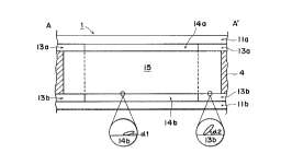
Figure 13 shows a second embodiment which is
a modification of the above-mentioned first
embodiment. In this embodiment, the electrodes 12a
supplied with scanning signals and the electrodes 12b
A
2121776
-34-
supplied with data signals are respectively extended
to the left and right peripheral regions and the upper
and lower peripheral regions. Accordingly, all the
four sides of peripheral regions can be supplied with
bipolar pulses for driving.
As a result, according to this embodiment,
the liquid crystal in the peripheral region is freed
from an inclination of assuming one stable state, and
the liquid crystal molecular movement thereat is made
smooth to provide a further enhanced effect of
preventing the yellowing.
(Third embodiment)
Figure 14 shows a third embodiment which is a
further modification of the second embodiment. In
this embodiment, the peripheral region 3 is separated
into an inner frame region 32a adjacent to the display
region 2 and an outer frame region 32b surrounding the
inner frame region 32a. Herein, the substrates lla-
and llb in the inner frame region 32a are subjected an
aligning treatment identical to that applied in the
display region 2, so that the resultant pretilt angle
is identical to that in the display region. On the
other hand, the substrates lla and llb in the outer
frame region 32b are subjected to a high-pretilt
treatment so that the liquid crystal in the outer
frame region 32b is caused to have a high pretilt
angle of at least 2~ degrees.
21217~fi
-35-
In this embodiment, the inner and outer frame
regions 32a and 32b are optically masked so that the
optical change caused by the liquid crystal in these
regions is made unnoticeable.
The masking may be performed by disposing a
light-interrupting (i.e., optically masking) film on
at least one of the substrates lla and llb at the
corresponding parts or by disposing the peripheral
regions at a part masked by a housing to which the
display panel is affixed.
(Fourth embodiment)
Figure 15 shows a fourth embodiment which is
a modification of the second embodiment. In this
embodiment, there are formed masked pixels each at an
intersection of a scanning electrode 12a and a data
electrode 12b in the peripheral region next to all
four sides of the display region. Further, four
corners 32c are filled with a sealing adhesive so that
the peripheral region is divided into four (upper,
lower, left and right) separate peripheral regions
including the masked pixels.
In this embodiment, all the electrodes
including those constituting the masked pixels are
supplied with bipolar pulses having positive and
negative voltages with respect to a certain reference
potential (e.g,, a potential allotted to a non-
selected scanning electrode).
-36-
As described above, the peripheral region
need not be disposed so as to surround all four sides
of the display region, and the prevention of yellowing
may be accomplished if the peripheral region is formed
to have a width of at least one pixel in the display
region. However, in consideration of repetitively
forming a specific display pattern, such as a stripe
pattern, or an all-black or all-white display state,
for a long period by a refresh drive, it is desirable
to form the peripheral region so as to surround the
entire periphery of the display region as shown in
Figures 11 to 14. In order to prevent the difficulty
accompanying a possible discontinuity in alignment at
the boundary between the low-pretilt alignment region
and the high-pretilt alignment region coinciding with
the edge of the display region and an ill effect
influencing the display quality in the display region,
it is preferred to dispose an inner frame region of a
low pretilt angle as in the embodiment of Figure 14.
In this instance, it is proper to provide the inner
frame region with an width of at least one pixel
similarly as the outer frame region. The masked
pixels formed in the embodiment of Figure 15 may be
formed as a low-pretilt region similarly as in the
display region.
Hereinbelow, some performances of the liquid
crystal devi.~e.according to the.present invention will
212177J3
-37-
be described based on experimental examples.
Example 1
Two glass substrates each in a planar size of
300 mm x 320 mm and a thickness of 1.1 mm were
respectively coated by sputtering with a ca. 1500 A-
thick ITO (indium tin oxide) film, which was then
patterned into stripe electrodes through lithographic
steps.
The stripe electrodes were further coated
with a ca. 900 A-thick Ta2O5 film for short circuit
prevention formed by sputtering. Then, as shown in
Figure 13, on a display region 2 and a peripheral
region 3 surrounding the display region 2 of each
substrate, an insulating film-precursor solution
containing about 450 A silica beads ("PAM 606EP" mfd.
by Shokubai Kasei K.K.) was applied by flexography and
baked at 300 ~C for ca. 1 hour to form a ca. 200 ~-
thick uneven insulating film. Then, on the entire
surface including the display region and the
peripheral region of each substrate, a polyimide-
precursor solution ("LQ1800", mfd. by Hitachi Kasei
K.K.) was applied by flexography and then baked at ca.
270 ~C for ca. 1 hour for imidation to form a ca. 200
A-thick polyimide alignment film, which was then
subjected to a rubbing treatment with a nylon pile
yarn-planted rubbing cloth except for the peripheral
region. Then, on one of the two substrates treated in
2121776
-38-
the above-described manner, ca. 1.5 ~m-dia. silica
beads were dispersed, and the other substrate on the
periphery of which a sealing adhesive had been applied
by flexography except for leaving an injection port 5
was applied, so that the rubbing directions on the
substrates were substantially parallel to each other
and in identical directions. (As a matter in general,
the rubbing directions can be disposed to intersect
each other). Thus, a blank panel having a display
region with a diagonal size of ca. 15 inches was
prepared. The panel at this stage still retained an
injection port 5, through which a liquid crystal
should be injected.
For the liquid crystal injection, the blank
panel was placed in an injection vessel, the interior
of which could be heated and compressed. Then, the
injection vessel was evacuated to form a vacuum within
the blank panel, and a liquid crystal was applied onto
the injection port of the panel.
Then, the temperature within the injection
vessel was raised to lower the viscosity of the liquid
crystal and the pressure within the vessel was
increased, thereby to inject the applied liquid
crystal into the panel through the injection port.
After completion of the liquid crystal injection, the
panel was cooled to an SmC* phase temperature and then
the injection port was plugged with an epoxy ~esin
2121~S
-39-
adhesive to prepare a liquid crystal panel of this
Example. The liquid crystal used was a pyrimidine-
based mixture ferroelectric liquid crystal showing the
following phase transition series.
-8.5 ~C 67 ~C 88 ~C 94 ~C
Cryst. ~ SmC* ~ SmA ~ Ch. >Iso.
Separately, in order to evaluate the pretilt
angles in the display region and the peripheral region
of the above-prepared liquid crystal panel, two types
of test liquid crystal panels were prepared in from
two pairs of substrates. Each pair of the substrates
had the same surface laminar structure as the pair of
substrates having provided the above-prepared panel of
this Example. Further, one pair of the substrates
were rubbed respectively in one direction in the same
manner as above but were applied to each with a
spacing of 20 ~m so that their rubbing directions were
parallel and opposite to each other, followed by
filling with a liquid crystal shown below, to provide
a test panel for measuring a pretilt angle
corresponding to the display region of the panel of
this Example. The other pair of substrates were not
rubbed in one direction and were applied with a
spacing of 20 ~m, followed by filling with the liquid
crystal shown below, to provide a test panel for
measuring a pretilt angle corresponding to the
peripheral region of the na.~el of Example.
212177$
-40-
The liquid crystal used was a liquid crystal
mixture assuming SmA phase in the temperature range of
10 - 55 ~C obtained by mixing 80 wt. % of a
ferroelectric liquid crystal ("CS-1014", mfd. by
Chisso K.K.) with 20 wt. % of a compound represented
by the following formula:
n-C3H7{~C~~~C5Hl l-n -
The pretilt angles measured in the above-
described manner were 17.5 degrees corresponding tothe display region and 58.5 degrees corresponding to
the peripheral region. In the actual liquid crystal
panel of this Example, a uniform alignment state was
formed in the display region, and an alignment state
providing substantially no bright state under cross
nicol polarizers was formed in the peripheral region.
Then, in order to evaluate the degree of
liquid crystal molecular movement in the liquid
crystal panel, two stripe areas Sl and S2 were formed
so as to extend perpendicularly to the rubbing
direction R of the panel as shown in Figure 16. In
the stripe area Sl, liquid crystal molecules were
uniformly oriented to one stable state assuming an
average molecular axis a and, in the stripe area S2,
liquid crystal molecules were uniformly oriented to
the other stable state assuming an average molecular
axis b. In this state, the panel was continually
212177~
-41-
supplied with 1/2 duty rectangular AC pulses of 25
~sec in pulse width and 40 volts in voltage amplitude
for ca. 20 hours. Thereafter, the cell thickness was
measured at two points A and B, i.e., two points on
opposite sides in the display region. As a result, no
cell thickness change was observed at all compared
with the cell thickness before the above electric
field application.
Comparative Example
A liquid crystal panel was prepared in the
same manner as in Example 1 except that the peripheral
region was not provided with the uneven insulating
film containing silica beads but was rubbed similarly
as in the display region. As a result of measurements
in the same manner as in Example 1, the pretilt angle
was 17.6 degrees at the display region and 17.3
degrees in the peripheral region. The alignment state
in both regions was a uniform alignment.
Then, the liquid crystal molecular movement
was evaluated in the same manner as in Example 1,
parts A and B showed cell thickness increases of 35 %
and 39 %, respectively, compared with the values
before the electric field application.
Example 2
In this example, a liquid crystal panel was
prepared by using a homeotropic aligning agent for
providing a homeot~opic alignment state in th~
2I21 77~
-42-
peripheral region. More specifically two substrates
were treated in the same manner as in Example 1 up to
the provision of the Ta2O5 film. Then, each substrate
was coated with a polyimide alignment film identical
to the one formed in Example 1. Then, two substrates
were subjected to a rubbing treatment, application to
each other and liquid crystal injection in a similar
manner as in Example 1 to prepare a liquid crystal
panel.
In the panel, a uniform alignment was formed
in the display region and a substantially homeotropic
alignment was formed in the peripheral region.
Then, the liquid crystal molecular movement
was evaluated in the same manner as in Example 1,
whereby no cell thickness change was observed at
either point A or point B compared with the state
before the electric field application.
Example 4
A liquid crystal panel having a planar
pattern as shown in Figure 13 and including a smectic
liquid crystal aligned in a bookshelf structure as
shown in Figure 6A was prepared in a similar manner as
in Example 1 except that the solution-application type
insulating film was formed without including the 450
~-dia. silica beads, a fluorine-containing
ferroelectric liquid crystal was used, and the
substrates were applied to each other so that their
2121 77~
-43-
rubbing directions were parallel and opposite to each
other.
The pretilt angle in the display region was 2
- 3 degrees and the pretilt angle in the peripheral
region was 58.5 degrees.
The yellowing or the cell thickness change
was not at all observed similarly as or even less than
in Example 1 while the inner surfaces of the
substrates in the peripheral region were not
roughened.
As a result of several experiments performed
while varying the rubbing intensity, excellent
performances were attained by panels showing a pretilt
angle not exceeding 5 degrees.
ExamPle 5
Example 1 was repeated while varying the
alignment film material and the rubbing intensities to
prepare several liquid crystal panels having a chevron
structure of Cl uniform alignment and various pretilt
angles in the display region.
In this case, good yellowing-preventing
effect was exhibited by liquid crystal panels showing
a pretilt angle in the display region of lO degrees or
higher, particularly 15 - 25 degrees, in combination
with the roughened inner surface provided by inclusion
of silica beads in the display region.
Example 6
2~2177~
-44-
In a similar manner as in Example 1, a liquid
crystal panel having a peripheral region including an
inner frame region 32a subjected to rubbing and an
outer frame region 32b not subjected to rubbing as
shown in Figure 14 was prepared.
The pretilt angle was 17 degrees in the inner
frame region.
The panel was evaluated with respect to the
liquid crystal molecular movement in the same manner
as in Example 1 with the proviso that the electrodes
constituting the inner frame region was supplied with
the same signals as in the display region.
As a result, the cell thickness change or
yellowing was not observed even after continuation of
the electric field application over 60 hours.
Example 7
Sample liquid crystal panels respectively
having the following characteristics were prepared by
appropriately modifying Example 1.
[Reference sample]
A panel having a planar pattern as shown in
Figure 11, having a pretilt angle of 18 degrees in
both display region and peripheral region, and having
roughened inner surfaces.
tSample A]
A panel having a planar pattern as shown in
Figure 11 and not provided with the insulating films
212177~
for surface roughening.
[Samples Bl and B2]
Panels having a planar pattern as shown in
Figure 11 including a liquid crystal in chevron
structure having pretilt angles of 18 degrees (Bl) and
8 degrees (B2), respectively, in the display region.
[Samples Cl and C2]
Panels having a planar pattern as shown in
Figure 11 including a liquid crystal in bookshelf
structure having pretilt angles of 2 degrees (Cl) and
6 degrees (C2), respectively, in the display region.
[Sample D]
A panel having a planar pattern as shown in
Figure 11 and a roughened inner surface.
[Sample E]
A panel having a planar pattern as shown in
Figure 11 and including adhesive beads dispersed in
addition to the spacer beads in the display region and
the peripheral region.
[Sample F]
A panel having a planar pattern as shown in
Figure 14 prepared without roughening of inner
surfaces.
[Samples G1 and G2]
Panels having a planar pattern as shown in
Figure 14 including a liquid crystal in chevron
structure having pretilt angles of 18 degrees (Gl) and
212~7~
-46-
8 degrees (G2), respectively, in the display region.
[Samples H1 and H2]
Panels having a planar pattern as shown in
Figure 14 including a liquid crystal in bookshelf
structure having pretilt angles of 2 degrees (Hl) and
6 degrees (H2), respectively, in the display region.
[Sample I]
A panel having a planar pattern as shown in
Figure 14 and a roughened inner surface.
[Sample J]
A panel having a planar pattern as shown in
Figure 14 and including adhesive beads dispersed in
addition to the spacer beads in the display region and
the peripheral region.
[Sample K]
A panel having a planar pattern as shown in
Figure 14, having roughened inner surfaces, including
a liquid crystal in a chevron structure with a pretilt
angle of 18 degrees and including adhesive beads.
[Sample L]
A panel having a planar pattern as shown in
Figure 15 prepared without roughening of inner
surfaces.
10 panels were prepared for each sample and
evaluated with respect to the items of (1) yellowing
after continuation of electric field application for
20 hours, 40 hours and 60 hours, respectively, after
212177~
-47-
the occurrence of yellowing for all lO panels of the
reference sample panel; (2) alignment as evaluated by
occurrence of alignment defects at the sides of the
display region; and (3) monostability as evaluated by
a difference in threshold between two directions of
switching between two stable states.
The results are summarized in the following
Table wherein o represents that 6 or more panels
showed a better performance, o represents that 2 - 5
panels showed a better performance, and a represents
that O - 1 panel showed a better performance,
respectively compared with the reference sample panel.
212177l~
-48-
Sample Yellowing after Align- Mono-
ment stability
20 hrs. 40 hrs. 60 hrs.
A o o a o
Bl ~ ~ ~ a o
B2 0 o O a a
C1 o o ~ ~ A
C2 0 o o
D 0 o o ~ ~
E 0 ~ o ~ a
F o o ~ o
G1 ~ ~ O
G2 ~ o o o Q
Hl ~ ~ 0 ~ a
H2 o o o o A
I o o o o
J o o o 0 A
K o 0 0 o o
L o ~ ~ ~
2~2177~
-49-
As described above, according to the present
invention, the pretilt angle in a peripheral region
surrounding a display region is made larger than that
in the display region or the liquid crystal in the
peripheral region is placed in a homeotropic alignment
state to prevent or suppress the occurrence of a local
pressure difference along a liquid crystal device
(panel) caused under continual application of an
electric field, thereby preventing the occurrence of a
cell thickness change or yellowing accompanying the
cell thickness change.