Note: Descriptions are shown in the official language in which they were submitted.
2122079
-
FIELD OF THE INVENTION
This invention relates to computers and in
particular to a universal interface to computers for
peripherals such as CD ROMS (compact disk read only
memories).
BACKGROUND TO THE INVENTION
A popular interface for computers is the SCSI
standard interface. Peripherals such as hard disk
drives and CD ROMS made by some manufacturers meet the
SCSI standard, but some do not. The SCSI standard
dictates the use of an SCSI interface circuit board
plugged into a slot of the computer, and a standard
socket that is externally available into which a plug
wired to a peripheral (device) may be connected. Pins
of the SCSI socket connect to predefined and standard
signal lines.
However, some manufacturers make peripherals that
are proprietary, and do not meet the SCSI standard. If
the computer owner wishes to use different peripherals
at different times, or wishes to change peripherals, a
different interface circuit board must be purchased with
a circuit and socket that matches that of the different
peripheral, and plugged into the computer, with the
attendant requirement to remove the cover of the
computer and risk damage to the computer, or at least
disruption to the physical environment of the user as
well as to work that must be done using the computer.
For proprietary CD ROMs, for example, a unique interface
circuit and a different connector is required for each
type of CD ROM. This precludes a design that supports
multiple types of CD ROMs without many circuit boards
and connectors and which use up valuable empty slots of
the computer motherboard.
21220~9
-
SUMMARY OF THE INVENTION
The present invention is a universal interface
which allows any one of plural peripherals to be plugged
into one or two sockets carried by the interface. Once
it has been installed, the only requirement to
accommodate a changed or new peripheral is to select it
from a menu using a software program; no further
physical interference with the computer is required.
One connector socket may be used to accommodate both
proprietary and SCSI connector plugs, or one socket may
be used for the proprietary plugs, and another may be
used for an SCSI plug.
In accordance with an embodiment of the
invention, a universal peripheral interface is comprised
of control logic circuits for a plurality of peripherals
carrying different signals on different pins of
respective peripheral connectors, a single interface
connector for mating with any of the peripheral
connectors, a first multiplexer for interfacing any of
the control logic circuits with the single interface
connector and for switching particular lines of each of
said control logic circuits carrying particular signals
to particular pins of said single connector, and means
for controlling the multiplexer to map said lines to
said particular pins of said single connector.
BRIEF INTRODUCTION TO THE DRAWINGS
A better understanding of the invention will be
obtained by reading the description of the invention
below, with reference to the following drawings, in
which:
Figure 1 is a basic block diagram illustrating an
SCSI design in accordance with the prior art,
Figure 2 is a basic block diagram illustrating a
design of plural CD ROM interfaces in accordance with
the prior art,
CA 02122079 1998-11-10
~,
Figure 3 is a basic block diagram of the present
invention,
Figure 4 is a more detailed block diagram of the
present invention,
Figure 5 is an even more detailed block diagram of
the present invention,
Figure 6 is a schematic diagram of a multiplexer
that can be used as part of the invention, and
Figure 7 is a block diagram of plural proprietary
CD ROM and an SCSI plugs and universal connector into
which they may be connected.
DETAILED DESCRIPTION OF THE INVENTION
Figure 1 illustrates a block diagram of a typical
SCSI CD-ROM interface. An SCSI CD-ROM 1 is connected
via a standard 50 pin SCSI connector assembly 3 (male
and female) to an SCSI controller 5 via an SCSI bus 6.
The controller is controlled in a well known manner by
miscellaneous logic circuit 7. Both controller and
logic circuit are connected to a host bus, usually via a
bus connector 8.
While the aforenoted system can allow connection of
an SCSI CD-ROM to the host computer system, it cannot
accommodate proprietary CD-ROMs, since proprietary
CD-ROMs have different signal requirements which are
transmitted and received on different on different leads
than are usual on the SCSI bus. In addition, each
proprietary CD-ROM is driven by a different form of
CD-ROM logic circuit. In order to use a proprietary
CD-ROM, a dedicated proprietary CD-ROM control logic
circuit is plugged into a computer, which carries a
CD-ROM connector into which a cable of the proprietary
CD-ROM is plugged. While the connector is typically 40
pin, each different proprietary CD-ROM transmits and
receives signals through different pins from others.
Z12207g
It is desirable for computer manufacturers to
provide computers into which any CD-ROM, proprietary or
standard SCSI versions, can be connected. To
accommodate this structure, computers contain "slots",
that is, empty connectors connected to the main bus of
the computer, into which various control or other
interface circuits can be plugged. Thus, for example,
to accommodate four different CD-ROM interface circuits
and a standard SCSI interface, five different interface
boards, each carrying its own interface connector are
plugged into different slots of the computer.
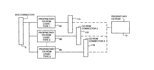
This structure is shown in Figure 2. Proprietary
interface circuit boards 9A - 9N, each carrying its own
connector, respectively llA - llN, are plugged into the
main bus of the host computer. Whatever proprietary
type of CD-ROM 13 the owner of the computer wishes may
be plugged into the corresponding connector llA - llN.
In this case either all or a large fraction of the slots
typically available on a desktop computer are used up
with the aforenoted mostly redundant and power wasting
circuitry.
The alternative is to use only a single proprietary
interface circuit 5 connected in the host computer as in
the system of Figure 1, restricting the owner to only
the CD-ROM that is matched to the interface.
Figure 3 is a block diagram of the present
invention. An universal interface 15 which is connected
to a universal connector 17 is used. The universal
interface 15 is connected to the host computer bus via
the usual connector 8, although it may be physically
connected to the host computer carried on-board the main
computer circuit board, and accessed via the main bus, a
peripheral bus, or by other means that will be
understood by persons skilled in the art.
212207~
-
Any proprietary peripheral 19 that can be
accommodated by the universal interface 15 may be
connected to the universal connector 15, including an
SCSI peripheral, depending on the connector 17 that is
used, as will be understood after understanding the
description below, which will be explained using CD-ROM
peripherals and interfaces as an example of the
preferred embodiment.
Figure 4 is a more detailed block diagram of the
system shown in Figure 3. The universal interface 15 is
comprised of specialized CD-ROM control logic circuits
2lA - 2lN. Each control logic circuit 2lA - 2lN
corresponds to elements 5 and 7 of Figure 1, and one can
be an SCSI control interface circuit, and are preferably
mounted on a single printed circuit board for connection
to the host bus, or are connected to the host in another
way, and can be mounted on the host motherboard.
Each logic circuit 2lA - 2lN is connected to the
input of a line multiplexer and pin switcher 23. A DIP
switch array 27 is connected to an address decoder 25.
The address decoder is connected to each of the logic
circuits 21A - 21N. A function control 29 is connected
to the address decoder 25, and to a control input of the
line multiplexer and pin switcher 23.
The single universal CD-ROM connector 17 is
connected to the output of the line multiplexer and pin
switcher 23.
In operation, the user selects which CD-ROM he or
she wishes to use. From a chart supplied by the
universal interface manufacturer, the user is told which
of the DIP switches in array 27 are to be closed to
designate that selected CD-ROM.
With the appropriate DIP switches 27 closed,
an address is presented to address decoder 25. The
decoder provides an enable signal to the addressed one
- 2122079
of the control logic circuits 21A - 21N, and as well,
signifies the address to function control 29. Function
control 29 in turn provides a selection signal to
multiplexer and switcher 23, in order to cause the
correct input lines corresponding to the addressed
control logic circuit 2lA - 2lN to be connected to
predetermined pins of the universal connector 17.
The selected CD-ROM that is connected to the
universal connector 17 is thus enabled to communicate
with the host computer and be controlled by the
appropriate control logic 2lA - 2lN.
It should be noted that rather than requiring the
use of DIP switch array 27, it could be dispensed with
if the address decoder is connected to the host computer
address conductors of the main bus, or be otherwise
controlled by the host computer. In this case, software
programs can cause supply of an appropriate address to
address decoder 25 instead of DIP switch 27. For
example, a software program can list a selection of
CD-ROMs, and the user can configure the universal
interface by selection of one from a menu list,
resulting in the software program causing downloading of
a corresponding address to address decoder 25.
The universal connector 17 may be of a type that
will accommodate both matching SCSI peripheral device
connectors and proprietary peripheral device connectors.
An SCSI connector is standardized with 50 pins, and a
CD-ROM proprietary connectors have typically 40 pins.
The universal connector may be physically designed with
50 pins, to accommodate both types of peripheral.
In addition, as will be described below, typically
CD-ROM connectors are comprised of two parallel rows of
pins, with signal carrying conductors connected to only
one of the rows, the other row being connected to
ground. It is preferred that the universal connector
21~7g
._
should have only one row of pins switched in multiplexer
and switcher 23, whereby a proprietary peripheral
connector which has its row of signal carrying pins on
the opposite side of the connector from the side used by
other peripheral connectors, may be properly connected
to and driven by the universal connector properly by
rotation of 180 degrees.
Figure 5 illustrates the multiplexer and pin
switcher 23 in more detail, and illustrates another
embodiment of the connector arrangement.
Address decoder 25 is connected to and receives
address signals from host bus 32, and decodes them to
define which CD ROM control logic circuit 2lA - 2lN
(including SCSI control logic circuit 2lM) is to be
selected. The address signal is applied to the host bus
upon selection of a particular CD ROM from a menu
displayed on the host display under control of an
application software installation program. Function
control 29 receives an enable signal from the host bus,
and applies a select signal via its output port 42 to a
select input port 40 of decoder 25. When it receives
the select signal, decoder 25 applies a select signal to
a select input port of a CD ROM resulting from the
decoding of the CD ROM address signal.
Function control 42 also applies control signals to
multiplexer 23, for control of the multiplexer 23.
Multiplexer 23 contains a signal receiving portion
44, an output multiplexer portion 46, and an input
portion 48. The output portion connects the leads of
the particular CD ROM control logic to the appropriate
leads leading to a pin of universal connector 17. The
input portion receives data signals from the CD ROM via
particular pins of the connector 17 and routes them to
the host bus 32 for receipt by the host processor and/or
2122Q79
the selected (enabled) CD ROM control logic circuit 21A
- 21N.
In accordance with an embodiment of the invention,
a second connector, a standard SCSI connector 50 is
connected in parallel with connector 17. As connector
17 will typically have 40 pins, and connector 50 has 50
pins, 40 of the 50 pins of connector 50 are connected
directly in parallel with the pins of connector 17, and
the remainder of the 50 pins are connected to other
leads of multiplexer 23 or to ground. The preferred
scheme will be described further below.
Indeed, rather than having two connectors each
having a different number of pins, connector 17 can have
the larger number of pins, e.g. 50, in order to allow an
SCSI connector to be connected to it, a proprietary 40
pin connector to be connected to it, a 50 pin
proprietary connector to be connected to it, or a
proprietary connector using a different number of pins
to be connected to it.
Figure 6 illustrates in more detail the multiplexer
interface with the universal connector. Plural leads
from each of the CD ROM control logic circuits are
connected to plural multiplexers, such as 52, together
forming multiplexer 23. Multiplexer 52 thus will be a
representative example of the remainder.
One of each of corresponding leads of the control
logic circuits are connected to corresponding inputs A,
B, C and D of a 4:1 signal multiplexer 52. It will be
recognized that since each of the control logic circuits
control a proprietary CD ROM drive, the signals carried
on the corresponding leads will be different. Thus for
example, from a Mitsumi CD ROM control circuit, the
signal on one lead will be its HD7 output, the signal on
the corresponding lead on a Sony CD ROM control circuit
will be its D0 output, the signal on the corresponding
2122Q79
-
lead on a Panasonic CD ROM control circuit will be its
RESETB output, and the signal on the corresponding lead
on an SCSI control circuit will be a -DB0 output.
However, each output is correct for its corresponding CD
ROM drive.
Multiplexer 52 receives control signals at its S0
and Sl inputs from the function control 29, which
signals are derived from the host bus 32. This signal
enables signals appearing at the particular input A, B,
C or D to be routed to its output.
The output of multiplexer 52 is applied to the
input of a tri-state switch, which has its enable
control input connected to host bus 32, Thus with a
control selection signal received on leads CDTYP0 and
CDTYPl which carry control signals from the function
control 29, a signal from one lead of the addressed
(selected) control logic circuit appears at the input of
tri-state switch 54. When tri-state switch 54 is
enabled, the signal that appears at its input is applied
to pin 53 of connector 17 (as well as connector 50, if
used).
Signals appearing at pin 53, which can be either
output from switch 54, or which can be input from a CD
ROM via pin 53, are passed through buffer 56, and are
applied to host bus 32 for reception by the host
multiplexer, and by the selected control logic circuit
if it requires it.
The following truth table lists representative
logic signals input to control inputs SO and Sl, carried
by corresponding leads CDTYPO and CDTYPl respectively:
CDTYPOCDTYPl CD ROM TYPE
0 0 Mitsumi
o l Sony
l O Panasonic
l l SCSI
Z122~79
-
Mapping between universal connector 17 and
different CD ROM mating connectors 58A - 58N is shown in
Figure 7. SCSI CD ROM connector 58M is also
illustrated. Each of representative mating CD ROM
connectors are labelled with the name of its CD ROM.
Thus for example while the Sony and Panasonic connectors
are 40 pin connectors similarly numbered, the Mitsumi CD
ROM has a 40 pin connector numbered oppositely.
Universal connector 17 is shown in the embodiment in
which it has 50 pins, numbered to match the SCSI
connector, although any of the mating connectors 598A -
58N can connect to it, flush against one end. The
Misumi mating connector is flipped 180 degrees, in order
to have its pins match the corresponding pins of
connector 17.
Table A illustrates signal functions on various
leads and corresponding pins of proprietary CD ROMs from
various manufacturers and of an SCSI standard against
the pinout and signals carried on those pins of a
preferred embodiment of the universal CD ROM connector
of the present invention. It has been found that the
signals of the CD ROMS are usually carried on one side
of its proprietary connector. The present invention
switches only signals, and not grounds. The universal
connector is wired such that the grounds are mainly on
one side of the connector. When the Mitusmi mating
connector is used, it is flipped 180 degrees relative to
the others, in order to have its correct pins connected
to the universal connector.
CA 02122079 1998-11-10
Universal CD-ROM Connector and Pin Mappint to Other CD-ROMs
Universal Universal
Pin No. CD-ROM Pin No. CD-ROM Mitsumi SONY Panasonic SCSI
Al GND Bl UNBl HD7 D0 RESETB -DB0
A2 GND B2 UNB2 HD6 Dl GND -DBl
A3 GND B3 UNB3 HD5 D2 DRVSLOB -DB2
A4 GND B4 UNB4 HD4 D3 DRBSLlB -DB3
A5 GND B5 UNB5 HD3 D4 HWRB -DB4
A6 GND B6 UNB6 HD2 D5 HRDB -DB5
A7 GND B7 UNB7 HDl D6 STCH -DB6
A8 GND B8 UNB8 HD0 D7 ADPCMB -DB7
A9 GND B9 UNB9 ENABL ERR DRQ -DBP
A10 GND B10 UNB10 IOW STENB DTENB GND
All GND Bll UNBll IOR DENB ENABLEB GND
A12 GND B12 UNB12 DACK DRQWB STENB GND
A13 GND B13 UNB13 DRQ DCMSB CMDB TERMP
A14 GND B14 UNB14 IRQ READB EOPB GND
A15 GND B15 UNB15 NC CMDWRB GND GND
A16 UNA16* B16 UNB16 NC DRVSLOB DB6 -ATN
A17 GND B17 UNB17 NC DRVSLlB DB5 GDN
A18 UNA18* B18 UNB18 NC DRVSL2B DB4 -BSY
Al9 GND Bl9 UNBl9 HAl DRVSL3B DB3 -ACK
A20 UNA20* B20 UNB20 HA0 RESETB DB2 -RST
A21 GND B21 UNB21 NC NC NC -MSG
A22 GND B22 UNB22 NC NC NC -SEL
A23 GND B23 UNB23 NC NC NC -C/D
A24 GND B24 UNB24 NC NC NC -REQ
A25 GND B25 UNB25 NC NC NC -I/O
*Note: UNA16, UNA18 & UNA20 are mapped to Panasonic D 7, DB4
and DBl
TABLE 1
2122079
A person understanding this invention may now
conceive of alternative structures and embodiments or
variations of the above. All of those which fall within
the scope of the claims appended hereto are considered
to be part of the present invention.