Note: Descriptions are shown in the official language in which they were submitted.
7 3
ALARM SYSTEM
Te~hnic~l Field
This invention relates to alarm systems, and more specifically, to
arrangements for enhancing trouble detection of such systems.
5 Problem
Most monitored element alarms are presented as a normally open
relay closure (closed contacts imply an alarm condition). The "P" wires (a pair
of wires) connecting this closure (at the "far" end) to the alarm sensing circuitry
(at the "near" end) is vulnerabie to being cut or shorted. A short is reported as a
10 false equipment alarm, which is acceptable since it attracts attention. A wire cut,
however, results in real equipment alarms not being reported. This may have
disastrous consequences.
Previous solutions use the normally closed relay contacts as
equipment alarms (open contacts imply an alarm condition). These detect cuts but15 not shorts. Also, multiplying of alarms is awkward since they have to be wired
in series. The normally open contacts are preferred by the industry. These
contacts can easily be wired in parallel to multiple alarms.
Solution
A simple electronic assembly (applique' circuit) is mounted at the
20 "far" end of the "P" wires in very close proximity to the monitored alarm
closure. This assembly has electrical characteristics similar to the alarm closure,
that is it can be open or closed (high or low impedance). The alarm sensing
circuitry periodically controls the state of this applique' (preferably using the
same "P" wire) to simulate an alarm condition and thereby testing the integrity of
25 the wire loop (See FIG. 1).
If alarms are to be multiplied the applique' circuit (e.g., CR2) is
placed at the farthest closure and the integrity of the whole wire run is
m~int~ined.
The arrangements can also be used with normally closed alarm
30 contacts by placing a normally closed test device in series with the alarm
contacts. In this case, a test is applied in order to detect wire shorts.
7 7 ~ ~ 73
In accordance with one aspect of the present invention there is
provided an alarm system comprising: means for responding to an alarm
indication through the closure of an electrical circuit; means for detecting said
closure; test means for closing said electrical circuit in response to a test signal;
5 and means for generating and tr~n~mittin~ said test signal to said test means;means for indicating an alarm in response to said means for detecting said
closure when said test means is not closing said electrical circuit; whereby said
test signal and test means are used to test whether said means for detecting is
connected to said means for responding.
In accordance with another aspect of the present invention there
is provided an alarm system comprising: means for responding to an alarm
indication through the opening of an electrical circuit; means for detecting said
opening; test means for opening said electrical circuit in response to a test signal;
means for generating and tr~n.~mitting said test signal to said test means; means
for indicating an alarm in response to said means for detecting said opening when
said test means is not opening said electrical circuit; whereby said test signal and
test means are used to test whether a connection between said means for
detecting and said means for responding has been short-circuited.
Brief Description of the Drawin~
FIG. 1 is a block diagram illustrating the basic concept of
applicants' invention;
FIG. 2 is a specific implementation of applicants' invention using
a zener diode as a device to be placed in parallel with a normally open alarm
indication contact;
FIG. 3 is an alternate implementation using a diode across the
alarm sensing contact and using a reverse voltage to test the integrity of the
connection to the alarm indication contact;
FIG. 4 illustrates the use of a testing device which is normally
not conducting, but which is rendered conducting by means of a voltage on a
separate test lead; and
~,
1 7 3
FIGS. 5-8 correspond to FIGS. 1-4 but are for use with an
~l~rming device which is normally closed; the testing device can be used to
detect short circuits across the access wires.
Detailed Descl;~lion
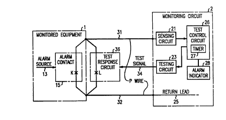
FIG. 1 illustrates the operation of the alarm system of applicants'
invention. Block 1 is the equipment being monitored. An alarm source 13 closes
relay contact 15 when an alarm indication is detected. Monitoring circuit 2 is
connected to the monitored equipment 1 by a pair of leads ("P" wires) 31 and
32. In parallel with alarrn contact 15 is a normally open test circuit 36 with
contact L for closing the circuit when a test signal 34 is applied. Testing circuit
23 applies the test signal and sensing circuit 21 senses whether either alarm
contact 15 is closed or contact L in test response circuit 36 is closed. Means (not
shown) for operating the test circuit periodically in order to ensure that the "P"
wires have not been cut. When the test circuit 23 sends test signal 34, then thesensing circuit 21 should detect a closure. In this case, the closure means that the
"P" wires have not been cut and is not an indication of an alarm. When the test
circuit does not send test signal 34 and the sensing circuit 21 senses a circuitclosure, then this is an indication that the alarrn contact 15 has been closed and
that an alarm indication exists. If the two "P" wires are shorted then sensing
circuit 21 will also sense a completion of the circuit; in this case, this is not an
alarm indication but an indication that the "P" wires have been shorted and mustbe repaired if the alarm indicator is to be useful.
The return lead 25 is connected to the second "P" wire (or
equivalent if common ground is used). In the configurations of FIGS. 2, 4, 6,
and 8, lead 25 is connected to ground. In the configurations of FIGS. 3 and 7,
lead 25 is a switched lead connected to ground or to battery via a resistor.
Test control circuit 26 is driven by a test control circuit including
a microprocessor (not shown) and a timer 27. Test control circuit 26 drives
testing circuit 23 and receives inputs from sensing circuit 21. Test control circuit
26 drives an alarm indicator 28 which can be audible, visual or graphic. Test
control circuits with their timers and alarm indicators are well known in the prior
art; one exarnple is the remote unit of the NJ-00508 Series Alarm Telemetry
11 7 ~
,~ .
System (trade mark) manufactured by AT&T (trade mark) Network Systems
Services. This remote unit can control the periodic application of tests to ensure
the integrity of the alarm system.
FIG. 2 shows the essential of one such alarm sensing circuit. It
5 consists of an opto-isolator 250 for TTL voltage level shifting, in order to drive a
circuit connected to the transistor of the opto-isolator, a current limi~ing resistor
(R1) (255), and a zener diode (257) with a normally open relay closure M across
it. Office battery (-Vs) is conn~cted at the anode of zener diode 257. Other types
of logic circuits such as CMOS can be used instead of TTL. A standard "P" wire
10 connects the monitored equipment alarm contact K to complete the loop to
ground. The applique' circuit consists of a similar zener diode 236 and is
connected across the alarm closure as shown. For simplicity, both zeners are
chosen with identical breakdown voltages (Vzl =Vz2=Vz). It is critical that the
chosen breakdown voltage (Vz) satisfies the condition Vs/2 < Vz < Vs.
For a typical -48 V alarrn monitoring office battery, 33 V
breakdown zeners are a good choice. Under normal conditions, both zener diodes
are off since the office battery (48 V) is less than the combined breakdown
voltage of the two zeners (66 V). This defines the "off" TTL state. When
equipment goes in an alarm condition, closure K shorts zener diode 236. This
causes the other zener diode 257 to break down since 48 V is now higher than itsbreakdown voltage of 33 V. The resulting current flows through the opto-isolatorLED 251 which in turn changes the TTL level to the "on" state, i.e., causes the
photo-transistor 253 to conduct. The monitoring circuitry will then report this as
an equipment alarm.
The controlling circuitry (not shown) will periodically activate
the closure of contact M to test the "P" wire loop. This shorts zener diode 257,which if all is well, will cause zener diode 236 to break down and generate a
similar "on" TTL state. If this is not the case, a "system failure" alarm will be
reported. The zener diode 236 in FIG. 2 and the alarm sensor is an optic isolator
250 comprising a photo diode 251 which emits light when current flows
therethrough and a photo transistor 253 which closes a circuit (not shown) when
- 3a-
it receives light from photo diode (LED) 251. Zener diode 257, is bypassed by
contact M (259) when it is used to test the integrity of the "P" wires. Vs is
insufficient to break down both of the zener diodes 257 and 236, but sufficient to
break down zener diode 236 alone. Therefore, if zener diode 257 is bypassed
when contact M (259) is operated, current should flow through photo diode 251
and zener diode 236. In this arrangement no separate test wire is required to
interconnect the monitored equipment and the sensing circuit. If a common
ground can be used to interconnect these two blocks, only a single wire is
required for their connection.
- 3b -
~,, ~.
2122173
" ,,
Applicants have found the zener diode approach to be the most
attractive, especially where a common ground exists, since only a single "P" wire is
required.
An alternative solution is shown in FIG. 3. Here the applique' circuit
5 consists of a single diode 336. The controlling circuit consists of a DPDT relay M
(354) which toggles office battery (-Vs) and ground across the "P" wires. Under
normal conditions, diode 336 will be reverse biased and the dual polarity opto-
isolator 350 will be off. During a loop test, relay M operates and the resultingchange of polarity forward biases diode 336 and LED 351 of opto-isolator 350 which
10 turns the opto-isolator to the "on" state. In a real alarm condition, closure of
contact K (15) will short diode 336 and rul~ard bias LED 352 of opto-isolator 350,
which also turns on the opto-isolator transistor 353.
FM. 3 thus substitutes the ability to apply reverse voltage to the "P"
wires using contacts of testing relay M (354). In the normal mode, the M relay is
15 released and no current flows through either diode 336 or diode 352 unless alarm
contact K (15) is operated. When the M relay 354 is operated, current flows through
diode 351, diode 336, and resistor 355, and photo transistor 353 becomes conductive
because current is flowing through photo diode 351 thus generating the light which
renders photo transistor 353 conductive. Note that the configuration of FIG. 3
20 requires two "P" wires since the common ground cannot be used without auxiliary.
FIG. 4 illustrates an arrangement wherein a separate test lead is used to
operate a test relay 471 or to make conductive a transistor 472 either of which is in
parallel with contact K (15).
FIG. 4 shows a case where an extra controlling wire is needed to
25 activate the applique' circuit and test the wire loop. The applique' circuit consists of
a SPST relay 471 or transistor 472. Again, when contact K (15) closes or when
contact 471 closes or transistor 472 is made conductive, opto-isolator 450 changes to
the"on" state.
Note that any number of items of monitored equipment may be placed
30 in parallel with the test contact L (36) of FIG. 1 or its equivalent in the other
diagrams and that with such an arrangement the alarm sensing circuit will indicate an
alarm if any of the monitored apparatus indicates an alarm or if the "P" wires are
shorted. Under test conditions, an open in the "P" wires can be detected.
FIGS. 5-8 correspond to FIGS. 1-4, but are for use with an alarm device
35 having a normally closed contact. The testing device, which is also normally closed
is in series with the alarm contact(s). (If there are several alarm contacts for one "P"
wire connection, the alarm contacts are in series in this configuration.) By opening
2122173
,_
the testing device and checking for the opening of the circuit, the presence of a short
circuit across the "P" wires can be detected; an open circuit (or alarm condition) is
detected if, in the normal (non-test) state, no current flows over the "P" wires.
It is to be understood that the above description is only of one prerelled
S embodiment of the invention. Numerous other arrangements may be devised by oneskilled in the art without departing from the scope of the invention. The invention is
thus limited only as defined in the accompanying claims.