Language selection

Search

Patent 2122176 Summary

Third-party information liability

Some of the information on this Web page has been provided by external sources. The Government of Canada is not responsible for the accuracy, reliability or currency of the information supplied by external sources. Users wishing to rely upon this information should consult directly with the source of the information. Content provided by external sources is not subject to official languages, privacy and accessibility requirements.

Claims and Abstract availability

Any discrepancies in the text and image of the Claims and Abstract are due to differing posting times. Text of the Claims and Abstract are posted:

  • At the time the application is open to public inspection;
  • At the time of issue of the patent (grant).
(12) Patent: (11) CA 2122176
(54) English Title: BI-METALLIC SWITCH ELEMENT
(54) French Title: ELEMENT DE COMMUTATEUR BIMETALLIQUE
Status: Expired and beyond the Period of Reversal
Bibliographic Data
(51) International Patent Classification (IPC):
  • H01H 37/52 (2006.01)
  • H01H 1/58 (2006.01)
  • H05B 41/06 (2006.01)
(72) Inventors :
  • KULIK, JOSEPH S. (United States of America)
  • VINCENT, ROBERT J. (United States of America)
  • BAZIN, SIMONE P. (United States of America)
(73) Owners :
  • GTE PRODUCTS CORPORATION
(71) Applicants :
  • GTE PRODUCTS CORPORATION (United States of America)
(74) Agent: R. WILLIAM WRAY & ASSOCIATES
(74) Associate agent:
(45) Issued: 2000-10-17
(22) Filed Date: 1994-04-26
(41) Open to Public Inspection: 1994-10-31
Examination requested: 1997-09-11
Availability of licence: N/A
Dedicated to the Public: N/A
(25) Language of filing: English

Patent Cooperation Treaty (PCT): No

(30) Application Priority Data:
Application No. Country/Territory Date
8/056,006 (United States of America) 1993-04-30

Abstracts

English Abstract


A bi-metallic switch element 10 has a contact wire 26 attached thereto by
means of
a plurality of crimps. A first crimp 28 applied at a first pressure fixes the
contact
wire to the element and a second crimp 30, formed at a lesser, more controlled
pressure aligns the contact wire in a predetermined location.


Claims

Note: Claims are shown in the official language in which they were submitted.

The embodiments of the invention in which an exclusive
property or privilege is claimed are defined as follows:
1. A bi-metallic switch element comprising: an
elongated bi-metallic member having a longitudinal axis
and comprised of a relatively high expansion material and
a relatively low expansion material in operative, intimate
contact with one another; and two spaced apart tunnels
formed in a first end of said member and projecting
upwardly from said high expansion material, said tunnels
being spaced apart from one another and aligned along said
longitudinal axis.
2. The bi-metallic switch element of Claim 1
wherein an elongated, electrically conductive contact wire
has one end thereof positioned in said tunnels.
3. The bi-metallic switch element of Claim 2
wherein another end of said contact wire projects beyond a
second end of said elongated bi-metallic element.
4. The bi-metallic switch element of Claim 3
wherein each of said tunnels is crimped to said wire, each
of said tunnels thereby separated into two tabs, said tabs
being asymmetric with respect to said longitudinal axis,
and the tabs of the first of said tunnels being asymmetric
with respect to the tabs of the second of said tunnels.
5. A bi-metallic switch element comprising: an
elongated bi-metallic member having a longitudinal axis
and comprised of a relatively high expansion material and
a relatively low expansion material in operative, intimate
contact with one another; two spaced apart tunnels formed
in a first end of said member and projecting upwardly from
said high expansion material, said tunnels being spaced
apart from one another and aligned along said longitudinal
axis; an elongated, electrically conductive contact wire
having one end thereof positioned in said tunnels; and

crimps formed in said tunnels, a first crimp formed in a
first of said tunnels fixing said wire to said bi-metallic
element and a second crimp formed in a second of said
tunnels positioning said wire in a predetermined location
relative to said bi-metallic element.

Description

Note: Descriptions are shown in the official language in which they were submitted.


... ". .v . s ...,. .. _ , . .. ~'Q.,:.n..; itko.',.. ~..m. . ,..r_. , >..,..
.~.. ".
r ~~z~~~~~~3u~5
~3-~-428
~I-METALLIC ~V~ITC~d ELEMENT
TEIrI-INICAL FIELD
This invention relates generally to bi-metallic switch elements and more
particularly
to such elements having better control over the location of a contact wire
which is a
part of the element. The element can form a part of a switch which can be
employed in the starting circuitry of high intensity discharge lamps.
EACKG~3gINI) ART
The basic elements of a bi-metal switch include at least a bi-metal member
which
usually is elongated and which can have a contact wire attached thereto.
Generally,
it is important that the contact wire be accurately positioned on the bi-
metal. Two
major forms of attachment have been employed in the past. A first simply
involves
welding the contact wire to the bi-metal and a second involves attaching the
wire by
means of a crimp. 'The latter method has been accomplished by stamping either
a
tunnel or a pair of tabs from the bi-metal, laying a wire in the opening thus
provided, and crimping the tabs or tunnel to the wire. ~Nhile these methods
provided an adequate holding means for the wire they did not provide for
accurate
location, since very often the force applied to fix the wire disturbed
whatever
previous location had been determined.
DISCLi0SURIE ~F 1'FIE INVENTI~N
It is, therefore, an object of the invention to obviate the disadvantages of
the prior
art.
It is another object of the invention to enhance bi-metal switch elements.
Yet another object of the invention is the enhancement of the operation of bi-
metal
switch elements.
These objects are accomplished, in one aspect of the invention, by the
provision of a
bi-metallic switch element which comprises an elongated bi-metallic member
having
a longitudinal axis and comprised of a relatively high expansion material and
a
- Page 1- 93428b/word/0(~8
SfA
,T,v
iis,

93-1-428
relatively low expansion material in operative, intimate contact with one
another.
'Two spaced apart tunnels are formed in a first end of the member and project
upwardly from the high expansion material. The tunnels are formed transverse
to
the longitudinal axis. An elongated, electrically conductive contact wire has
one
end thereof positioned in the tunnels. Crimps are formed in the tunnels with a
first
crimp being formed in a first of the tunnels fixing the wire to the bi-
metallic element
and a second crimp being forned in a second of the tunnels for positioning the
wire
in a predetermined location relative to the bi-metallic element.
The employment of the plural tunnels allows for the use of differential
pressures for
each of the crimps and provides for control over the location of the contact
wire.
BRIEF 1)ES~RIPTI~1~ ~F TIE 1DRAWINGS
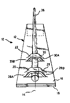
Fig. 1 is a perspective view of a bi-metallic element having a pair of contact
wire
receiving tunnels formed in one end thereof;
Fig. 2 is a perspective view of a bi-metallic element with a contact wire
crimped in
the tunnels; and
Fig. 3 is a side elevational view of a bi-metallic element illustrating a
placement of
the contact wire.
BEST l~~I)E FCDR CAR~t'YI1V~ ~UT ~E Il~N1'lf~N
Fox a better understanding of the present invention, together with other and
further
objects, advantages arid capabilities thereof, reference is made to the
following
disclosure and appended claims taken in conjunction with the above-described
drawings.
Referring now to the drawings with greater particularity, there is shown in
Figs. 2
and 3 a bi-metallic switch element 10 which comprises an elongated bi-metallic
member 12, shown by itself in Fig. 1, having a longitudinal axis 14 and
comprised of
a relatively high expansion material 16 and a relatively low expansion
material 18 in
operative, intimate contact with one another. A suitable material is ASTM B388
Type TMS. Two spaced apart tunnels 20 and 22, respectively, axe formed in a
first
- Page 2 - 93428b/word/0008

93-1-428
end 24 of member 12 and project upwardly from the high expansion material 16.
An
opposite end of the element 12 has a right angle bend formed therein to
provide a
wall 23. The tunnels are formed transversely to the longitudinal axis. An
elongated, electrically conductive contact wire 26, which preferably is formed
from a
high tensile tungsten wire such as NS-55I~1 which is avaliable from ~SRAM
SLYVANIA, Townada, Pennsylvania 18848, has one end thereof positioned in the
tunnels. (As used herein, high tensile designates wire having a strength of 67-
72
gm/mg/200m). A first crimp 28 is formed in a first of the tunnels, e.g., 20,
to fix the
wire 26 to the bi-metallic element 12. The crimp 28 causes an asymmetric
rupture
of the tunnel, as is shown in Fig.2, and provides what appears to be a pair of
tabs
28a and 28b. The asymmetry is caused by the use of an offset clamping punch. A
first, relatively high pressure is employed to form the crimp 28. A second
crimp 30
is formed in the second tunnel 22 and is used to position the wire in a
predetermined position relative to the bi-metallic element 12. 'The second
crimp 30
also provides an asymmetric rupture of the tunnel to form tabs 30a and 30b.
These
latter tabs ark asymmetric with respect to the tabs 28a and 28b and both sets
of tabs
are asymmetric with respect to the centerline 14.
The second crimp 30 is preferably formed at a lower pressure than the first
crimp to
aid in positioning the location of the wire. This can be accomplished by
making the
second set of clamping tools slightly longer than the first set. In the
embodiment of
the invention shown and described below, the second set of tools can be 0.003"
(0.0076mm) longer than the first set.
Ttte preferred location of the contact wire 26 is contiguous with the surface
of the
element 12 and aligned along centerline 14. As shown in Fig.3 by the dimension
"a", a small tolerance is acceptable. In a preferred form of the invention the
tolerance should be no greater than lmm for a switch element having a length
of
0.875" (2.223mm) and a width of 0.125" (0.318mrn). 'The tunnels have a width
of
about 0.040" (0.102mm) and can be separated by about 0.U46" -0.050" (0.117-
0.127mm). The transverse length of the tunnels is about 0.0625" (0.158mm).
While not limited thereto, the switch 10 described herein has greatly improved
the
operation of high intensity discharge lamps by providing an accurate cycle
time over
the life of the lamps.
- Page 3 - 93428b/word/0048

93-1-428
While there have been shown and described what are at present considered to be
the preferred embodiments of the invention, it will be apparent to those
skilled in
the axt that various changes and modifications can be made herein without
departing from the scope of the invention as defined by the appended claims.
_ page 4 - 93428b/word/0008

Representative Drawing
A single figure which represents the drawing illustrating the invention.
Administrative Status

2024-08-01:As part of the Next Generation Patents (NGP) transition, the Canadian Patents Database (CPD) now contains a more detailed Event History, which replicates the Event Log of our new back-office solution.

Please note that "Inactive:" events refers to events no longer in use in our new back-office solution.

For a clearer understanding of the status of the application/patent presented on this page, the site Disclaimer , as well as the definitions for Patent , Event History , Maintenance Fee  and Payment History  should be consulted.

Event History

Description Date
Time Limit for Reversal Expired 2008-04-28
Letter Sent 2007-04-26
Inactive: IPC from MCD 2006-03-11
Grant by Issuance 2000-10-17
Inactive: Cover page published 2000-10-16
Pre-grant 2000-07-19
Inactive: Final fee received 2000-07-19
Notice of Allowance is Issued 2000-01-21
Letter Sent 2000-01-21
Notice of Allowance is Issued 2000-01-21
Inactive: Approved for allowance (AFA) 1999-12-29
Amendment Received - Voluntary Amendment 1999-08-05
Inactive: S.30(2) Rules - Examiner requisition 1999-05-05
Inactive: Office letter 1998-06-05
Inactive: Delete abandonment 1998-06-05
Deemed Abandoned - Failure to Respond to Maintenance Fee Notice 1998-04-27
Letter Sent 1997-10-23
Inactive: Application prosecuted on TS as of Log entry date 1997-10-20
Inactive: Status info is complete as of Log entry date 1997-10-20
Request for Examination Requirements Determined Compliant 1997-09-11
All Requirements for Examination Determined Compliant 1997-09-11
Deemed Abandoned - Failure to Respond to Maintenance Fee Notice 1997-04-28
Inactive: Adhoc Request Documented 1997-04-28
Application Published (Open to Public Inspection) 1994-10-31

Abandonment History

Abandonment Date Reason Reinstatement Date
1998-04-27
1997-04-28

Maintenance Fee

The last payment was received on 2000-04-05

Note : If the full payment has not been received on or before the date indicated, a further fee may be required which may be one of the following

  • the reinstatement fee;
  • the late payment fee; or
  • additional fee to reverse deemed expiry.

Please refer to the CIPO Patent Fees web page to see all current fee amounts.

Fee History

Fee Type Anniversary Year Due Date Paid Date
Request for examination - standard 1997-09-11
MF (application, 4th anniv.) - standard 04 1998-04-27 1998-04-27
MF (application, 5th anniv.) - standard 05 1999-04-26 1999-04-15
MF (application, 6th anniv.) - standard 06 2000-04-26 2000-04-05
Final fee - standard 2000-07-19
MF (patent, 7th anniv.) - standard 2001-04-26 2001-04-02
MF (patent, 8th anniv.) - standard 2002-04-26 2002-04-03
MF (patent, 9th anniv.) - standard 2003-04-28 2003-04-02
MF (patent, 10th anniv.) - standard 2004-04-26 2004-04-01
MF (patent, 11th anniv.) - standard 2005-04-26 2005-04-01
MF (patent, 12th anniv.) - standard 2006-04-26 2006-03-30
Owners on Record

Note: Records showing the ownership history in alphabetical order.

Current Owners on Record
GTE PRODUCTS CORPORATION
Past Owners on Record
JOSEPH S. KULIK
ROBERT J. VINCENT
SIMONE P. BAZIN
Past Owners that do not appear in the "Owners on Record" listing will appear in other documentation within the application.
Documents

To view selected files, please enter reCAPTCHA code :


To view images, click a link in the Document Description column. To download the documents, select one or more checkboxes in the first column and then click the "Download Selected in PDF format (Zip Archive)" or the "Download Selected as Single PDF" button.

List of published and non-published patent-specific documents on the CPD .

If you have any difficulty accessing content, you can call the Client Service Centre at 1-866-997-1936 or send them an e-mail at CIPO Client Service Centre.


Document
Description 
Date
(yyyy-mm-dd) 
Number of pages   Size of Image (KB) 
Abstract 1995-08-26 1 38
Claims 1995-08-26 2 90
Description 1995-08-26 4 216
Drawings 1995-08-26 1 38
Cover Page 1995-08-26 1 46
Claims 1999-08-05 2 63
Cover Page 2000-09-21 1 28
Representative drawing 1997-08-15 1 10
Representative drawing 2000-09-21 1 9
Acknowledgement of Request for Examination 1997-10-23 1 178
Commissioner's Notice - Application Found Allowable 2000-01-21 1 166
Maintenance Fee Notice 2007-06-07 1 173
Correspondence 2000-07-19 1 34
Fees 1999-04-15 1 38
Fees 1997-04-24 1 53
Fees 1996-03-27 1 62