Note: Descriptions are shown in the official language in which they were submitted.
2~22561
BACKGROUND OF THE INV~N~l~ION
1 - Field of the Invention
! The present invention is generally concerned with
decisions to be arrived at in a receive subsystem of a
multistate modulation-demodulation system. The present
invention is more particularly concerned with a decision device
lo ~ for a non-linear modulation-demodulation system, typically a
frequency modulation-demodulation system.
2 - Description of the Prior Art
In a receive subsystem a decision device is connected on
the output side of a demodulator device. The decision device
determines successive symbols received at respective successive
sampling times by comparing the level of the demodulated signal
with predetermined thresholds.
FIGS. 1 and 2 respectively show a transmit subsystem 1 and
a receive subsystem 2 together forming a frequency modulation-
demodulation system with four states known as the 4FSK or four-
frequency shift keying system.
Referring to FIG. 1, the transmit subsystem 1 comprises a
serial-to-parallel converter 10, a digital-to-analog converter
11, a low-pass filter 12 and a voltage-controlled oscillator
13. If the link between the subsystems 1 and 2 is of a radio
type, an output of the transmit subsystem 1 and an input of the
receive subsystem 2 are connected to respective antennas 14 and
20.
2~22~1
The receive subsystem 2 comprises, connected to the antenna 20,
a frequency converter stage 21 in which the signal frequency is
converted to an intermediate frequency (I.F.), a band-pass
filter 22, a frequency discriminator 23, a low-pass filter 24,
a decision device 25 and a parallel-to-serial converter 26.
A baseband serial binary signal Sb to be transmitted is
converted in the converter 10 into a signal made up of symbol
words ak on two parallel binary elements. Each word ak is
associated with two binary elements of the serial signal Sb and
o is part of a symbol word alphabet {00, 01, 10, 11~. Each word
ak is converted in the digital-to-analog converter 11 into a
symbol Sk having one of four levels -3, -1, 1 or 3 according to
the respective symbol word 00, 10, 01 or 11. The signal formed
by the successive symbols Sk ls applied to an input of the
oscillator 13 through the filter 12 which smooths the spectrum
-- of the signal made up of the successive symbols. The
oscillator 13 produces a 4FSK modulated signal with four states
assuming a respective one of four frequencies FO-3Fd, FO-Fd,
FO+Fd, F0+3Fd, according to the respective level -3, -1, 1 or
2c +3 of the symbol Sk. F0 and Fd are respectively the nominal
frequency of the oscillator 13 and a predetermined frequency
difference.
The 4FSK modulated signal is transmitted by the transmit
antenna 14, then received by the receive antenna 20. It is fed
from the antenna 20 to the frequency converter stage 21 which
converts the spectrum of the received 4FSK modulated signal
into an intermediate frequency signal SFI. The signal SFI is
filtered by the band-pass filter 22 in a narrow frequency
I band which is centered on an intermediate center frequency
corresponding to the frequency FO converted. The filtered
signal SF at the output of the filter 22 is fed to an input
of the discriminator 23. By carrying out time
2122~1
- differentiations the discriminator 23 discriminates between the
frequencies in the filtered signal SF and delivers a signal SD
whose levels are substantially equal to -3, -1, 1, 3 according
to the symbols Sk transmitted. This signal SD is low-pass
filtered in the filter 24 to produce an analog signal S*. In
the decision device 25 the signal S* is sampled at the
frequency of the transmitted symbols Sk. The levels assumed by
, the signal S* at the sampling times are compared to thresholds
in the device 25 which delivers the symbol words ak according
o to the result of these comparisons. By applying parallel-to-
serial conversion to the symbol words ak the converter 26
delivels the original binary signal Sb transmitted.
FIG. 3 is a diagram showing the theoretical eye diagram of
a baseband signal S* resulting from four-state frequency
modulation and demodulation, as delivered by the low-pass
filter 24 in the receive subsystem 2. In this theoretical
diagram, the vertical aperture d of each of the upper eye Os,
; the center eye Oc and the lower eye Oi is maximal and equal to
the difference between the respective levels of two adjacent
~ symbols, i.e., d=(3~ 1)=-1-(-3)=2. A theoretical diagram
like this represents null intersymbol interference at the
sampling times. In the decision device 25 the baseband signal
S* delivered by the filter 24 is sampled at meaningful sampling
times IE and the levels of the resulting samples are compared
to three thresholds Ss, Sc and Si shown on the righthand side
in FIG. 3. There are four distinct outcomes for each sample.
If the level of the sample is above the upper threshold Ss, the
decision device 25 delivers the sample word 1Ill'' associated
with the symbol Sk = 3; if the sample level lies between the
upper threshold Ss and the center threshold Sc, the decision
2~22~1
device 25 produces the symbol word "01" associated with the
symbol Sk = 1; if the sample level lies between the center
threshold Sc and the lower threshold Si, the symbol word "10"
is produced by the device 25; finally, for a symbol level below
the threshold Si, the symbol word "00" associated with the
symbol Sk = -3 is produced.
In the decision device 25 of a receive subsystem of the
prior art the decision thresholds Ss, Sc and Si are constant
and the level of the received signal S* is varied relative to
o the constant decision thresholds. This variation may be the
result of a "displacement" and/or an "amplification" of the
baseband signal S*.
As shown in FIG. 5, the means used to vary the baseband
signal S* are in the form of an amplifier 27 with automatic
gain control (AGC) and an adder 2~8, both on the input side of
the decision device 25 in the receive subsystem 2, and a
comparator 29. Inputs of the comparator 29 respectively
receive, at the symbol transmission frequency, the samples ak*
resulting from the sampling 25a of the baseband signal S* and
~ the corresponding symbols Sk produced by the decision device
25. / ~ comparing Vthe signals ak*/~ ~ S~ the co~parator
-~ produces two error signals ~1 and ~ 2 respec~ y ~ lied to a
--~ -- control input of the amplifier 27 and to a second input of the
adder 28. In response, the amplifier 27 amplifies the received
signal S* and the adder 28 displaces the DC component in the
received signal, and therefore in the baseband signal S*, so
that the level of each sample ak* is slaved to the level of the
corresponding symbol Sk. The variation of the signal S*
reduces the error rate in the received binary signal Sb at the
~o output of the parallel-to-serial converter 26.
x
2~5~:l
The displacement operation of the signal S* by the adder
28 can be regarded as a simultaneous displacement or
translation of the three thresholds Ss, Sc and Si.
The amplification of the signal S* by the amplifier 27 can
be regarded as two respective translations of equal magnitude
and opposite sign of the thresholds Ss and Si relative to the
threshold Sc.
Controlling the amplitude of the signal S* according to
constant predetermined thresholds Ss, Sc and Si by means of an
o automatic gain control amplifier 27 produces a result that is
satisfactory in terms of error rate reduction provided that the
upper and lower eye patterns Os and Oi in the eye diagram have
apertures _ which are substantially equal and symmetrical ~bout
a horizontal axis corresponding to the threshold Sc in FIG. 3.
In practise, although this condition is met by linear type
modulation systems, such as amplitude modulation systems, it is
not met by non-linear modulation systems, typically frequency
modulation systems.
As shown in the eye diagram of FIG. 4 relating to four-
state frequency modulation, the upper eye pattern Os and thelower eye pattern oi do not have the above-stated symmetry and
- eye dimension characteristics. FIG. 4 also shows the
theoretical optimal upper and lower thresholds Ss and Si for
, null intersymbol interference. It can be seen that reducing
the error rate to a minimal value entails a negligible increase
A of the upper threshold Ss to yield a modified upper threshold
SMs and a more marked decrease D of the lower threshold Si to
yield a modified lower threshold SMi. This modification of the
thresholds Ss and Si to yield the thresholds SMs and SMi does
not result from equal and opposite translations of the
respective thresholds Ss and Si relative to the center
threshold Sc, as is effected by an automatic
"
21 Z~6 1
gain control amplifier 27 in the prior art.
OBJECT OF THE INVENTION
The main object of this invention is to provide a decision
device suitable for non-linear modulation systems in which a
baseband signal resulting from modulation and demodulation has
on average and at meaningful sampling times levels which are
asymmetric relative to a null level axis. This signal
characteristic is reflected in an asymmetric eye diagram. It
results from asymmetric filtering in the transmit and receive
subsystems of a frequency modulation type non-linear modulation
system.
SUMMARY OF THE ~Nv~N~ION
; Accordingly, a decision device for producing at a symbol
frequency symbols according to levels of a baseband signal
I resulting from demodulation of a multistate frequency modulated~0 signal, comprises
voltage divider means having first and second inputs to
which are respectively applied lower and upper voltages
delimiting a voltage range for establishing plural voltages in
the voltage range,
adding means for adding said baseband signal to a midpoint
voltage which is substantially equal to the mean of the lower
and upper voltages and established by the voltage divider means
thereby producing a transposed signal,
plural comparator means for comparing the transposed
~ signal with the plural voltages respectively to produce
comparison result signals,
encoder means for deri~ing control words at the
f,
2~22~1
symbol frequency, each control word being dependent on
comparison result signals which are representative of a level
of the baseband signal relative to lower, center and upper
decision thresholds corresponding to three respective voltages
of the plural voltages, and
first and second control means for respectively and
. independ~ntly slaving the lower and upper voltages as a
function of the control words.
o The first and second control means correct the decisions
at the level of the lower eye pattern oi and the upper eye
pattern Os. To this end, said first and second control means
respectively comprise
first and second logic means for deriving respective first
and second three-state error signals,
the first, respectively second error signal being at two
predetermined states only in response to first, respectively
second predetermined control words conditioned by first,
respectively second two levels of the transposed signal
situated on either side of the lower, respectively upper
decision threshold,
first and second integrators for integrating the first and
second error signals thereby producing first and second
integrated signals, and
first and second adders for respectively adding the first
integrated signal with a lower nominal voltage and the second
integrated signal with an upper nominal voltage, in order to
establish the lower and upper voltages.
The invention also attempts to remedy the asymmetry of the
center eye pattern Oi in the eye diagram (FIG. 4). The
decision device then comprises third control means for
controlling, according to the control words and the
2~561
; midpoint voltage, said center decision threshold to be added in
place of the midpoint voltage to said baseband signal in the
adding means. The third control means can comprise, like the
first and second control means, a third logic means for
deriving a third error signal having at least two states, the
third error signal being at two predetermined states in
response to third two predetermined control words conditioned
by third two levels of the transposed signal situated to either
side of the midpoint voltage, i.e. either side of the center
o decision voltage,
a third integrator for integrating said third error signal
thereby producing a third integrated signal, and
a third adder for adding said third integrated signal with
the midpoint voltage in order to establish said center decision
threshold.
The encoder means comprises plural means for sampling at
the symbol frequency the comparison result signals thereby
producing sampled comparison signals, and means for encoding
the sampled comparison signals thereby deriving a rank word
identifying the highest rank of comparator means having
produced a comparison result signal with a predetermined logic
level, at least three most significant bits of the rank words
constituting the control words.
In one embodiment of the invention each of the sampling
means is a D-type flip-flop.
The decision device further comprises a rhythm recovering
circuit receiving one bit of the rank word in order to produce
a sampling signal clocking sampling in said sampling means.
In practise, the voltage divider means, the comparator
- 30 means and the encoder means are included in an analog-to-
digital converter integrated circuit.
q:
2t22~61
BRIEF DESCRIPTION OF THE DRAWINGS
The foregoing and other objects, features and advantages
of the invention will be apparent from the following detailed
description of several embodiments of the invention with
reference to the corresponding accompanying drawings, the first
five figures in which have already been explained, in which
FIGS. 1 and 2 are respectively block diagrams showing a
transmit subsystem and a receive subsystem forming a four-state
lo non-linear modulation-demodulation system ;
FIG. 3 is a theoretical eye diagram for a baseband signal
resulting from demodulation of a four-state frequency modulated
--- signal ;
FIG. 4 is an eye diagram as observed in practise for the
baseband signal distorted by successive filtering and resulting
from demodulation of a four-state frequency modulated signal ;
FIG. 5 is a block diagram of a decision device in which
the baseband signal is controlled according to the prior art,
included in a receive subsystem of the type shown in FIG. 2 ;
FIG. 6 is a detailed block diagram of an adaptive
threshold decision device according to the invention ; and
FIG. 7 is a table of control signals associated with a
theoretical eye diagram analogous to that in FIG. 3 and
. produced by a logic circuit included in the decision device
shown in FIG. 6.
DETAILED DESCRIPTION OF THE PREFERRED ENBODIMENTS
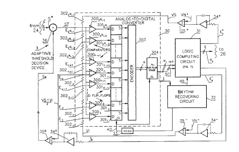
Referring to FIG. 6, an adaptive threshold decision
~122~6:1
device 3 according to the invention comprises an analog-to-
digital converter 30, a logic computing circuit 31, a rhythm
recovering circuit 32, a voltage controlled oscillator 33,
three integrators 34~, 34 and 34+ and four adders 35~, 35 ,
35+ and 36.
The N-bit analog-to-digital converter 30 with accuracy N
comprises 2N-1 comparators 3001 through 3002N_1, 2N-l D-type
flip-flops 3011 through 3012N_1, a series of 2N resistors 3020
through 3022N_l, an encoder 303 and a stage 304 with N D-type
o flip-flops in parallel, N being a predetermined integer at less
equal to 3.
A lower voltage VI and an upper voltage VS are
, respectively applied to two terminals of the series of 2N
f resistors 3020 through 3022N_1, which form a voltage divider
stage. Said two terminals are one terminal of the first
resistor 3020 and one terminal of the last resistor 3022N_l.
The limit voltages VI and VS delimit a range of quantization of
a received signal by the converter 30. 2N-l terminals common
to paired successive resistors (302n_1, 302n)~ where a iS
between 1 and 2N, are at respective voltages E1 through E2N_l
increasing in the quantization range (VS-VI). All the
resistors 3020 through 3022N_1 have the same resistance R. The
, voltage at the terminals of each of the resistors 3020 through
3022N_1 is equal to (VS-VI)/2N and defines the quantization
step, i.e., the accuracy of the converter 30.
Positive terminals (+) of the 2N-1 comparators 3001
through 3002N_l receive an analog signal ST transposed into the
baseband by transposition in the adder 36 of the signal S* at
~ the output of the filter 24 included in the receive subsystem 2
(FIG. 2). The adder 36 is preferably preceded by a capacitor C
rejecting any DC component in the signal S*. The voltages E1
through ~2N_1 increasing in arithmetic progression produced at
~12256 ~
the common terminals of the series-connected resistors are
applied to negative (-) terminals of the comparators 3001
through 3002N_1. Each comparator 300n, n being between 1 and
2N-1, produces a logic signal representative at any time of the
result of comparing the voltage En with the transposed signal
ST. Thus for a level of the transposed signal ST lying between
the voltages En and En+1, all the comparators 300m~ where m<n,
produce a signal at the "1" state and all the comparators 300
where m>n+1, produce a signal at the "0" state.
o The outputs of the comparators 3001 through 3002N_1 are
respectively connected to data inputs D of the 2N-1 D-type
sampling flip-flops 3011 through 3012N_1. A clock input CL of
these 2N-1 flip-flops 3011 through 3012N_1 receives a clock
signal H2 produced by the voltage-controlled oscillator 33.
The corresponding "1" and "0" states at the outputs of the
comparators 3001 through 3002N_1 are respectively stored at
data outputs S of the 2N D-type flip-flops in response to each
active edge of the signal H2 and during a period of this clock
signal H2. The outputs S of the 2N D-type flip-flops are
; respectively connected to 2N-1 inputs of the encoder 303 which
derives a N-bit flip-flop rank word corresponding to the
highest rank of the D-type flip-flops whose outputs have
produced a "1" state. In the previously mentioned example
relating to a level of the transposed signal ST lying between
the voltages En and En+l, the rank word derived by the encoder
303 corresponds to the rank n in binary code of the flip-flop
301n. If the signal VT lies between the voltages VI and
E1 = VI + ~VS - VI)/2N, the bits of the rank word are all equal
to "0".
30 IThe N-bit rank word derived by the encoder is stored in
the stage 304 by N flip-flops clocked by the clock signal H2.
12
- .
s~i
-
~22~
Only I=3 of the N parallel bits at the outputs of the stage 304
are applied to an input port of the computing logic circuit 31.
These I=3 bits are the three most significant bits (MSB) SCN_1,
- SCN_2 and SCN_3 of the N-bit rank word and form a word of
control signal SC.
Note that one bit of the rank word at the output of the
flip-flop stage 304, preferably the most significant bit (MSB),
is applied to an input of the rhythm recovering circuit 32
which produces a clock signal H1 and controls the voltage-
controlled oscillator 33 producing the clock signal H2. The
clock signal H2 is therefore slaved to the phase of the symbols
received for sampling the comparison result signals in the D-
type flip-flops 3001-3002N_1.
A table of control signals derived by the logic computing
circuit 31 is described next with reference to FIG. 7. The
logic computing circuit is clocked by the clock signal H1 which
typica'ly has a frequency equal to half the frequency of the
clock signal H2. As shown in the three lefthand columns of the
table, the I = 3 most significant bits SCN_l, SCN_2 and SCN_3
, of the rank word forming the control signal SC are sufficient
to describe each level of the transposed signal ST relative to,
~ firstly, the theoretical levels of the symbols Sk in the set {-
3, -1, +1, +3} and, secondly, the decision thresholds Si, Sc
and Ss. In the case of the embodiment described the lower and
upper thresholds Si and Ss respectively correspond to a common
terminal voltage Ei substantially equal to VI+(VS-VI)/4 and a
common terminal voltage Es substantially equal to VS-(VS-VI)/4.
The circuit 31 produces at the symbol transmission frequency
I H1, two-bit symbol words ak, a three-state lower threshold
adjustment error logic signal ~ k , a three-state upper
threshold adjustment error signal ~ k ~ and a
-
~2~61
displacement error bipolar signal Y k for transposing the
baseband signal S*. Each of the two-bit symbol words ak is
produced by the circuit 31 as a function of the first two most
significant bits (MSB) SCN_l and SCN_2 of the I=3 bits of the
control signal SC, these two bits representing the sampling
level of the signal ST relative to the three thresholds Si, Sc
and Ss.
The third error signal r k assumes the state "+1" or "-l"
according to the state "1" or "0" of the least significant bit
o (LSB) SCN_3 of the control signal SC.
The second error signal ~ k systematically assumes a null
value "0" except for sets of three bits SCN_1, SCN_2, SCN_3
equal to "101" and "110" of the control signal SC for which it
respectively assumes the states "-1" and "+1". These sets of
three bits "101" and "110" correspond to levels of the signal
ST near and on either side of the upper threshold Ss.
The first error signal ~ k systematically assumes a null
value "0", except for sèts of three bits SCN_1, SCN_2, SCN_3
--- equal to "001" and "010" of the control signal SC for which it
respectively assumes the states "-1" and "+1". These sets of
three bits "001" and "010" correspond to levels of the signal
- ST near and on either side of the lower threshold Si.
The error signal r k is integrated over a period
significantly greater than the period of the clock signal H1 by
the integrator 34~ to produce an integrated displacement error
signal which is applied to a first input of the adder 35~. A
second input of the adder 35~ is at a midpoint voltage
(VS + VI)/2 at the terminal common to the resistors 3022N_1 and
30 . 3022N-1_1, which is substantially equal to En in the embodiment
shown in FIG. 6. The output of the adder 35~ is connected to a
first input of the adder 36 a second input of which receives
14
--
- -'
21~2~B~
the baseband signal S*. The component En added to the signal
', S* by the adder 36 transposes the baseband signal S* into a
positive voltage range coinciding with the quantization range
, of the analog-to-digital converter 30, typically lying between
0 volts and 5 volts.
The first error signal ~ k iS time integrated by the
integrator 34~ analogous to the integrator 34~ to produce an
integrated lower error signal which is applied to a first input
of the adder 35~. A second input of the adder 3S- is at a
o lower nominal voltage VN-. The adder 35~ produces the lower
voltage VI which is applied to said terminal of the first
resistor 3020.
The second error signal ~ k iS time integrated by the
integrator 34+ analogous to the integrator 34~ to produce an
integrated upper error signal which is applied to a first input
of the adder 35+. A second input of the adder 35+ is at an
upper nominal voltage VN+. The adder 35+ produces the upper
voltage VS applied to said terminal of the last resistor
3022N_1.
The operation of the adaptive threshold decision device 3
and the functions of the three voltage control loops are now
described in detail with reference to FIGS. 6 and 7. The first
voltage control loop comprises the integrator 34~, the adder
35~ and the adder 36. The second voltage control loop
comprises the integrator 34~ and the adder 35~. The third
voltage control loop comprises the integrator 34+ and the adder
35+.
Referring to FIG. 7, the lower error signal ~ k goes from
the "-1" state to the "+1" state when the control signal SC
.~
~ 15
i
i
21225~1
changes from "001" to "010", and vice versa. These values
correspond to two quantization levels of the baseband signal ST
in the flip-flops 3011 through 3022N_l respectively below and
above the lower threshold Si. By virtue of the integration of
the error signal ~ k the lower limit voltage VI is slaved to
the binary configurations "001" and "010" in the control signal
SC and thus to the distortion of the baseband signal S* in the
lower part oi of the eye diagram. On average, if the error
signal ~ ~ remains in the "-1" state, this indicates that the
o 1 threshold Si is too high. In thls case the lower limit voltage
VI is reduced to a value substantially less than the lower
nominal value VN-, which also reduces the lower threshold Si -
[VI + (VS - VI/4]. On the other hand, if the error signal ~ k
remains in the "+1" state, the voltage VI is increased to a
value substantially greater than VN-, which increases the lower
threshold Si.
The above remarks apply by analogy to the control of the
upper limit voltage VS and the threshold Ss _ VS - (VS - VI)/4
according to the "101" and "110" configurations of the control
signal SC by means of the error signal ~ ~ in the control loop
comprising the components 34~ and 35~ and thus according to the
distortion of the baseband signal S* in the upper part Os of
the eye diagram.
In a variant offering lower performance, in the absence of
the center threshold Sc control loop, i.e. of the integrator
34~ and the adder 35~, the midpoint of the series of resistors
3020 through 3022N_1 is connected directly to the first input
of the adder 36. The midpoint voltage (VS - VI)/2 then varies
with the average of the controlled limit voltages VI and VS so
that the converter 30 operates linearly in its positive
quantization range.
16
2~22~6~
,......
However, referring to FIG. 6, the integrator 34~ and the
adder 35~ contribute to controlling the center threshold Sc
according to central distortions in the baseband signal S* and
in particular for the eye pattern Oc. In this way, if after
integration, the third error signal ~k tends towards "-1",
respectively towards "+1", this indicates that the threshold
Sc, i.e. the voltage ~En~ at the midpoint of the series of
resistors, is too high, respectively too low, and that it must
be reduced, respectively increased.
o The center threshold Sc therefore tracks the variations in
the limit voltages VI and VS whilst being controlled according
to the distortions of the "-1" and "1" symbols of the received
4FSK signal.
In an alternative embodiment the third error signal Yk is
a three-level signal which is in the "0" state except for the
"011" and "100" combinations of the control signal SC for which
it respectively assumes the "-1" and "+1" states.
Compared to the prior art, the adaptive threshold decision
device 3 according to the invention does not effect global
transposition of the baseband signal by means of an automatic
gain control amplifier. In other words, the device 3 does not
multiply simultaneously by the same voltage gain the thresholds
Si, Sc and Ss. Rather, it adjusts each of these three
thresholds independently to provide the best match to the
asymmetric nature of the eye diagram and therefore to the
levels assumed by the baseband signal S* at successive sampling
times according to the symbols received.