Note: Descriptions are shown in the official language in which they were submitted.
CA 02122605 2002-04-09
1
HIGH TEMPERATURE
SUPERCONDUCTOR-DIELECTRIC RESONATOR
FIET:D :OF T~jE INVENTION
This invention relates to microwave resonators
formed of high temperature superconductor and dielectric
materials as well as to electronic circuits that employ
those microwa~ce resonators.
BACICGR~UND OF TFIE INVFNTjs"1,~1
Microwave resonators are known'for use .in time and
frequency standards, frequency stable elements, as well
as building blocks for pas ive devices such as filtersw
and ahe like. The performance of ahe microwave
resonator is gauged by its Q-value, expressed as
Q=2~t fp * (Storage energy/Loss power) , (1)
where fp is the resonant frequency of the microwave
resonator. (See Engineering Electromagnetics, William H.
Hayt; Jr., 4th edition, 1981, McGraw-Hill, New York,
p. 472). As showm in Equation (1), the Q-valve of the
;microwave resonator caw be increased by reducing the loss
power associated with factors such as conductor loss,
dielectric loss, and radiation loss.
Low temperature (T~), such .as 4 K, superconducting
microwave resonators which employ a auperconducting
cavity made of Nb are known. to have Q-values from about
106 to 109. (See V. B. 8raginskii, et al: "the
Properties of Superconducting Resonators on Sapphire",
IEEE Trans. on Magn: Vo1.;17, No. 1, P955, 19$1, as a
reference.) Although low T~ Nb microwave resonators
have high Q-value , they must operate at very low
temperatures (below 9 K). These microwave resonators
35. require use of curved cavity walls. Curved cavity walls
2~ 226 0 5
2
of materials which have a high T~, of for example 77 K,
however, are difficult ~o produce. Gn the other hand,
high Q-value microwave =esonators formed merely from a
dielectric without an associated conducting medium a'_so
have high Q-values (see D. G. Blair, et al: "High Q
Microwave Properties of a Sapphire Ring Resonator",
J. Phys . D : Appl . Phys . , ~,,~, P1651, 1982 . ) However, the
problems associated with the far reaching evanescent
fields make them very bulky and vulnerable to
microphonic effect, wh'_ch limits the applications.
Curtis, J. A. et al., 1991 IEEE MTT-S ~aternationa'_
Microwave Symposium Digest, Vol. 2, pp. 447-450,
June 10-14, 1991, 3oston, MA, U.S. discloses hybrid
dielectric/high temperature superconductor resonators
and filter configurations using these resonators. .or
the TEpll mode resonators disclosed the Q-value is about
200,000 at 20 K. Pao, ;.. et al., 1988 _EEE MTT-S
International Microwave Symposium Digest, Vol. 1,
pp. 457-458, May 25-27, 1988, New York, NY, U.S.
disclose a superconductor-dielectric resonator based on
a sapphire tube loaded with two plates of Y-Ba-Cu oxides
wherein a Q-factor of 105 to 106 may be achieved using a
X01$ or HplS mode. Kogami, Y. et al., 1991 IEEE MTT-S
International Microwave Symposium Digest, Voi. 3,
pp. 1345-1348, June 10-14, 1991, Boston, MA, U.S.
teaches a bandpass filter using two TMp,$ mode
dielectric rod resonators oriented axially in a high
temperature superconductor cylinder having a Q value ef
150,000 at 20 K. St. Martin, J. et al., Electornics
Letters, Vol. 26, No. 24, November 22, 1990,
pp. 2015-2016 discloses a dielectric resonator antenna
consisting of a HEM11$ mode circular dielectric
resonator fed by a microstrip feedline through a
coupling aperture in the ground plant between them.
The need therefore exists for microwave resonator
made of high T~ , such as 77 K, superconductor that have
SU~T1TUTE S~iEET
2122605
2A
Q-values comparable to low T~ superconducting microwave
resonators made of Nb.
BRIEF DESCRIPTIGN OF THE DRAWINGS
Figures 1(a) and 1(b) show a vertical cross section
of superconducting microwave resonator and a holding
device for that resonator.
Figure 2 is a schematic block diagram of a
frequency stable element for oscillators that employs
the microwave resonator of the invention.
Figures 3(a) and 3(b) show configurations or
filters using superconducting microwave resonators
according to the inver_tion.
Figure 4 shows the Q-values of a superconducting
microwave resonator of t'.~.e invention that employ
YBa2Cu30 superconductor and sapphire dielectric.
Figure 5 shows t'~:e Q-values of a superconducti~:g
microwave resonator o= the invention that employs
TlBaCaCuO superconductor and sapphire dielectric.
Figure 6 shows the relationship oz Q-value of the
resonator to the size or the dielectric.
Figure 7 shows cross sectional views of an
alternative embodiment of a device for holding the
microwave resonators of the invention.
SUESTiTUTE SHEET
WO 93/09575 - 3 PCT/US92/09635
~1~2605
Figure 8 shows a vertical cross section of a
further embodiment of a device for holding the microwave
resonator of the invention.
Figure 9 shows a vertical cross section of a
further alternative embodiment of a holding device for
the microwave resonators of the invention.
Figure 10 shows a vertical cross section of a
further embodiment of a holding device for the microwave
resonators of the invention.
Figures 11(a)-11(d) show top views of alternative
embodiments for coupling the microwave resonators of the
invention to an electronic circuit.
Figure 12 shows a top view of a coupling mechanism
that utilizes dual couplings for coupling the microwave
resonators of the invention to an electronic circuit.
Figure 13 shows a top view of a coupling of the
microwave resonator of the invention to an electronic
circuit integrated onto the back side of the substrate.
Figure 14 shows a vertical cross section of an
alternative embodiment of the microwave resonators of
the invention.
SL1_M_NtARY OF THE INVENTTON
The invention is directed to high temperature
superconductor-dielectric microwave resonators, to
holding devices for those resonators, coupling of those
resonators to electronic circuits, and to their methods
of manufacture. The superconducting microwave resonator
of the invention employ a superconducting film on
substrates positioned on a dielectric. The holding
devices include a variety of configurations, such as, a
spring loaded device. The microwave resonators can be
readily coupled to electronic circuits. The
superconducting microwave resonators have Q values that
are as high as low temperature microwave resonators
formed of Nb, but operate at much higher temperature.
WO 93/09575 ~, ~ ~ PCT/US92/09635
In accordance with the invention, a high
temperature superconducting microwave resonator
comprising a dielectric and a plurality of substrates
bearing a coating of high temperature superconducting
material is provided. The substrates are positioned
relative to the dielectric to enable the coating to
contact said dielectric.
The invention also includes devices for retaining
the configuration of the superconducting microwave
resonator of the invention. These devices comprise
means to retain the relative positions of the substrate
and the dielectric during use of the microwave resonator
in an electrical circuit. These devices further
comprise means for coupling of the microwave resonator
to electrical circuits.
The invention is further directed to a method for
coupling the superconducting microwave resonator of the
invention to an electric circuit by employing means
positioned on the substrate for transferring
electromagnetic energy between the dielectric of the
superconducting microwave resonator and an electrical
circuit via openings on the superconducting films and
coupling lines.
The invention is still further directed to passive
devices such as filters that are formed of a plurality
of dielectrics positioned between a plurality of
substrates bearing a coating of. high temperature
superconducting material, or wherein the dielectrics and
substrates are in alternating positions relative to each
other.
DETAILED DESCRIPTION OF THE INVENTInN
Having briefly summarized the invention, the
invention will now be described in detail by reference
to the following specification and non-limiting
examples. Unless otherwise specified, all percentages
WO 93/09575 ~ 1 6 O 5 5 PCT/US92/09635
are by weight and all temperatures are in degrees
Kelvin.
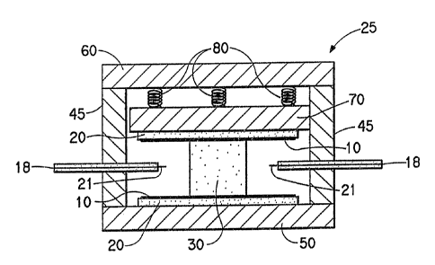
Figure 1 shows superconducting microwave resonator
and a holding device for that resonator. As shown in
Figures 1(a) and 1(b), a superconducting microwave
resonator 100 with cavity 90 is provided in the form of
substrates 20 bearing superconducting film 10
positioned on dielectric 30. Substrate 20 is a single
crystal that has a lattice matched to superconductor
film 10. Preferably, substrates 20 are formed of
LaA103, NdGa03, Mg0 and the like.
Generally, superconductor film 10 may be formed
from any high T~ superconducting material that has a
surface resistance (Rs) that is at least ten times less
than that of copper at any specific operating
temperature. T~ can be determined by the "eddy current
method" using a LakeShore Superconductor Screening
System, Model No. 7500. Surface resistance of
superconducting film 10 can be measured by the method
described in Wilker et al., "5-GHz High-Temperature-
Superconductor Resonators with High Q and Low Power
Dependence up to 90 K", IEEE, Trans. on Microwave Theory
and Techniques, Vol. 39, No. 9, September 1991,
pp. 1462-1467. Generally, superconductor film 10 is
formed from materials such as YBaCuO (123), TlBaCaCuO
(2212 or 2223), TlPbSrCaCuO (1212 or 1223), or the like.
Superconducting film 10 can be deposited onto
substrate 20 by methods known in the art. See, for
example, Holstein et al., "Preparation and
Characterization of T12Ba2CaCu20g Films on 100 LaA103",
IEEE, Trans. Magn., Vol. 27, pp. 1568-1572, 1991 and
Laubacher et al., "Processing and Yield of YBa2Cu30~_X
Thin Films and Devices Produced with a BaF2 Process",
IEEE, Trans. Magn., Vol. 27, pp. 1418-1421, 1991.
WO 93/09575 21 2 ~ ~ ~ ~ pCT/US92/09635
Generally, the thickness of film 10 is in the range of
0.2 to 1.0 micron, preferably 0.5 to 0.8 micron.
Microwave resonator 100 is formed by positioning
substrates 20 bearing superconducting film 10 on
dielectric 30. Substrates 20 can be placed on the
surface of dielectric 30, or, alternatively, low loss
adhesive materials may be employed. Polymethyl
methacrylate optionally may be deposited onto the
surface of superconducting film 10 to more firmly bond
dielectric 30, as well as to protect superconducting
film 10.
Dielectric 30 may be provided in a variety of
shapes. Preferably, dielectric 30 is in the form of
circular cylinders or polygons. Dielectric 30 may be
formed of any dielectric material with a dielectric
constant er>1. Such dielectric materials include, for
example, sapphire, fused quartz, and the like.
Generally, these dielectric materials have a loss factor
(tan 8) of from 10-6 to 10'9 at cryogenic temperatures.
The ~r and tan 8 of the dielectric material can be
measured by methods known in the art. See, for example,
Sucher et al., "Handbook of Microwave Measurements",
Polytechnic Press, Third Edition, 1963, Vol. III,
Chapter 9, pp. 496-596.
The configuration of the microwave resonator 100,
when in use, is maintained by holding device 25. The
holding device can be any embodiment that maintains the
relative positions of the components of the resonator
during thermal cycling associated with use of the
resonator. Figure 1(a) shows a first embodiment of a
holding device that employs spring loading. As shown in
Figure 1(a), the configuration of microwave resonator
100 is maintained by holding device 25. Holding device
25 includes sidewalls 45, bottom plate 50, top lid 60,
pressure plate 70, and load springs 80. Load springs
WO 93/09575 21 2 2 6 0 5 ' ~ PCT/US92/09635
80 are sufficiently strong to retain the configuration
of the microwave resonator during thermal cycling. Load
springs 80 preferably are formed of nonmagnetic material
in order to prevent disturbing the radio frequency
fields in the resonator to achieve the highest possible
Q-values. Load springs 80 preferably are formed of Be-
Cu alloys.
Parts 45, 50, 60 and 70 of holding device 25 are
made of thermally and electrically conductive materials
in order to reduce.radio frequency loss as well as to
enable efficient cooling of resonator 100. Parts 45,
50, 60 and 70 therefore may be formed of, for example,
oxygen fired copper, aluminum, silver, preferably oxygen
fired copper or aluminum.
The high T~ superconductor-dielectric microwave
resonators of the invention are capable of attaining
extremely high Q-values, due in part, to the ability of
substrate 20 bearing film 10 to prevent axial radio
frequency fields from extending beyond the London
penetration depth of the superconducting film 10. This
is accomplished where substrates 20 are substantially
greater than the diameter of dielectric 30 so that radio
frequency fields are confined within the cavity region
between substrates 20.
The high Q-value superconducting microwave
resonators provided by the invention have a variety of
potential applications. Typically, these resonators may
be employed in applications such as filters,
oscillators, as well as radio frequency energy storage
devices.
The microwave resonators of the invention also may
be employed as frequency stable elements to reduce the
phase noise for oscillators. As shown in Figure 2,
circuit 51 employs a microwave resonator 100 of the
invention that is inserted into a closed feedback loop
PCT/US92/09635
WO 93/09575
of, preferably, a low noise amplifier 15. Where the
product of the gain of amplifier 15 and the insertion
loss of resonator 100 is greater than one, and where
the total phase of the closed loop, as adjusted by phase
shifter 17, is a multiple of 2n, then, due to the
extremely high Q-values of the superconducting microwave
resonators of the invention, the oscillator can be made
to oscillate at the microwave resonator's resonant
frequency to yield lower phase noise in the oscillator.
The superconducting microwave resonators of the
invention also may be employed to provide highly stable
frequencies suitable for secondary standards for
frequency or time. Since the microwave resonator has an
extremely high Q-value and operates at a constant
cryogenic temperature, the microwave resonator has a
very stable resonate frequency that makes the resonator
useful for serving as a secondary standard.
The superconducting microwave resonators of the
invention further may be employed as building blocks in
passive devices such as filters. Examples of such
filters are shown in Figures 3 (a) and 3 (b) . As
illustrated in Figure 3(a), filter 110 is shown in the
form of a series of dielectrics 30 sandwiched between
substrates 20 bearing superconducting films 10.
Coupling between dielectrics 30 is achieved by the
evanescent fields of dielectrics 30. Coupling of filter
10 to electronic circuits (not shown) can be achieved by
coaxial cable 18 bearing coupling loop 21.
Figure 3(b) shows an alternative embodiment of a
filter. As shown in Figure 3(b), filter 120 employs a
series of dielectrics 30. Coupling between dielectrics
30 is achieved by the evanescent fields of dielectrics
30 via openings (not shown) on substrates 20. Coupling
of filter 120 to an electronic circuit (not shown) can
be achieved by couplings 13. Couplings 13 can be
WO 93/09575 2 ~ 2 2 6 0 5 ' ~'' PCT/US92/09635
coaxial lines, waveguides, or other transmission lines.
In either of the embodiments of Figures 3(a) or 3(b),
the high Q-values of the superconducting microwave
resonators reduces the in-band insertion loss of the
filter so as to make the skirt of the frequency response
curve of the filter steeper.
An additional application of the superconducting,
microwave resonators of the invention is to measure the
surface impedance (Zs) of superconductor materials and
the complex dielectric constant Er s Er' - jEr" of
dielectric materials, where Zs and e= have been
determined by measurement of fp and Q at two differing
modes in accordance with methods known in the art.
Generally, high Q-values for the superconducting
microwave resonators of the invention may be obtained by
selecting the proper electromagnetic modes to prevent
flow of radio frequency current across the edges of
superconducting films 10. These proper modes are TEoin
modes where the radial mode index has a value of
i=1,2,3,... and the axial mode index has a value of
n=1,2,3,... All TEoin modes have only circular radio
frequency currents that do not cross the edge of films
10.
Having selected the specific electromagnetic mode
of the microwave resonator, the Q and the resonant
frequency fp for the microwave resonator can be
calculated by solving Maxwell's Equations for the
boundary conditions of the resonator, as is known in the
art.
The loss power associated with parasitic coupling
to low Q-value modes such as non-TEpin modes or case
modes may be minimized in the microwave resonators of
the invention by assuring that substrates 20 are flat
and parallel to within a tolerance of less than 1°.
Loss power also may be minimized by ensuring that the
WO 93/09575 ~ ~ "l0 ~ ~ ~ PCT/US92/09635
C-axis of anisotropic materials such as sapphire, when
employed as dielectric 30, is perpendicular to substrate
20 to within t 5°, preferably 1°.
As also is shown in Figure 1(a), microwave
resonator 100 can be coupled to an electric circuit
(not shown) by coaxial cable 18 that includes coupling
loop 21 protruding into cavity 90 of microwave
resonator 100. The orientation of coupling loop 21 and
the depth of insertion of coaxial cable 18 into cavity
90 readily can be adjusted to ensure coupling to the
electronic circuit.
In a preferred aspect of the invention,
superconducting film is formed by epitaxially depositing
0.5 micron superconducting films of T12Ba2Ca1Cu20 or
YBa2Cu30 on 2 inch diameter substrates of LaA103
positioned on cylindrical dielectrics of sapphire. The
superconducting film is deposited so that the C-axis of
the film is perpendicular to the surface of the
substrate. The dielectrics of sapphire typically
measure 0.625 inch diameter by 0.276 inch tall, 0.625
inch diameter by 0.552 inch tall, or 1.00 inch diameter
by 0.472 inch tall. The substrates and dielectric are
retained in position by a holding device formed of
oxygen free copper. Coupling of the microwave resonator
to an electrical circuit can be achieved by inserting
two 0.087 inch diameter copper or stainless steel, 50
ohm coaxial cables with coupling loops made of extended
inner conductor into the cavity of the resonator. The
surface of the coupling loops is perpendicular to the
vertical axis of the sapphire dielectric to enable
selective coupling to the TEpll (i=1, n=1) mode of the
dielectric.
The Q values of the above described microwave
resonators, when employing YBa2Cu30 as the
superconducting film, are shown in Figure 4. As shown
T
WO 93/09575
212 2 6 ~ 5 11 PCT/tJS92/09635
in Figure 4, Q values of 5 million, 1.5 million, and
0.25 million are found at temperatures of 4.2 K, 20 K
and 50 K, respectively. The Q values of the above
described microwave resonators, when employing
T12Ba2Ca1Cu20 as the superconducting film, are shown in
Figure 5. As shown in Figure 5, Q values of 6 million,
3 million, and 1.3 million are found at temperatures of
20 K, 50 K, and 77 K, respectively.
The dependence of Q values of the above described
microwave resonators that employ T12Ba2CalCu20 as the
superconducting film on the size of the sapphire
dielectric is shown in Figure 6. As shown in Figure 6,
the Q values increase from 3 million to 6 million with
increasing size of the sapphire dielectric.
Device 25 shown in Figure 1(a) that employs spring
loading is only illustrative. Other means for holding
microwave resonator 100 are shown below.
Figures 7(a) and 7(b) show an alternative
embodiment for holding the microwave resonators of the
invention. As shown in Figure 7, the microwave
resonator is held by holding device 27. Device 27 is
indentical to device 25 except that, as shown in Figure
7(a), spring loaded holding device 27 employs three
dielectric rods 35 positioned 120° relative to each
other to further support dielectric 30. Dielectric rods
are inserted through side walls 47 of holding device
27 into cavity 95. Dielectric rods 35 have a low loss
and a dielectric constant less than that of dielectric
30. The tips of rods 35 are pointed to minimize contact
30 area with dielectric 30 to minimize loss power.
A further embodiment of a device for holding the
microwave resonators of the invention is shown in Figure
8. As set forth in Figure 8, the microwave resonator is
retained in position by holding device 28. Holding
35 device 28 is identical to holding device 25 except for
WO 93/09575 ~ 1 2 2 6 0 5
12 P~/US92/09635
the additional use of retainer 77. As shown in Figure 8,
substrate 20 bearing superconducting film 10 is
positioned on bottom-plate 50. Dielectric 30 is
positioned on substrate 20. Retainer 77 is positioned
about dielectric 30. Retainer 77 contacts sidewalls 45
and superconducting film 10 on substrate 20. Retainer 77
and side walls 45 have openings for receiving coaxial
cables 18. Cables 18 have loops 21 for coupling of the
resonator to an electric circuit(not shown). Retainer 77
is formed of materials that have low dielectric constant
of nearly 1 and low tan 8 of <10'4. As shown in Figure 8,
retainer ?7 is hollow, and is solid near sidewalls 45
where the electrical fields are minimum. The wall
thickness of retainer 77 is minimized to reduce the
contact area between retainer 77 and dielectric 30 to
minimize loss power.
Still yet another embodiment of a holder device for
the microwave resonators of the invention is shown in
Figure 9. Holding device 29 shown in Figure 9 is
identical to holding device 25 except for the use of
additional dielectric 65. As shown in Figure 9, cavity
91 between dielectric 30 and the interior surface of
sidewall 45 of device 25 is filled with dielectric
material 65. Dielectric material 65 has a tan 8 of less
than 10-5. Examples of dielectric material 65 include
styrofoam, porotic teflon, and the like.
Figure 10 shows a further embodiment of a holding
device suitable for use with the superconducting
microwave resonators of the invention. Holding device
24 shown in Figure 10 is identical to holding device 25
except for additional use of holding pins 71. As shown
in Figure 10, pins 71, formed of low tan b dielectric
materials such as sapphire, quartz, polymers,
polytetrafluoroethylene ("teflon"), "Delrin", registered
trademark of E. I. du Pont de Nemours and Company, and
I T
WO 93/09575 ~ ~ 13 PCT/US92/09635
~1 2260 5
the like are inserted into substrate 20 bearing
superconducting film 10 and into dielectric 30.
Figures 11(a) to 11(d) show alternative embodiments
for coupling of the microwave resonators of the
invention to an electronic circuit (not shown).
Generally, the embodiments shown in Figures 11(a)-11(c)
entail use of substrates that bear superconducting films
on the surfaces of the substrate that directly contacts
dielectric 30. Openings are provided on the
superconducting film on the side which directly contacts
dielectric 30. A coupling device is located over the
opening on surface of the substrate that does not
contact dielectric 30.
Figure 11(a) shows a microstrip line coupling
mechanism for coupling of the microwave resonators of
the invention to an electronic circuit (not shown). In
Figure 11(a), microstrip line 15 is formed by depositing
superconducting film material on that surface of
substrate 20 that is remote to dielectric 30.
Microstrip line 15 serves as the lead to an electronic
circuit (not shown). Opening 12 is provided in film 10
on the surface of substrate 20 that contacts dielectric
30. Opening 12 extends through film 10 but not through
substrate 20. Opening 12 does not contact dielectric
30 in order to minimize the effects of magnetic fields
on dielectric 30. Opening 12 is parallel to the local
magnetic field. Coupling is achieved by magnetic field
leakage through opening 12 to line 15. Microstrip line
15 extends over opening 12 by a distance of 7l/4, where
is the wavelength of the radio frequency field at the
operating frequency of the resonator.
Figure 11(b) shows a coplanar line coupling
mechanism for coupling the microwave resonators of the
invention to an electronic circuit (not shown). The
coplanar line coupling is formed by depositing
WO 93/09575 ~ ~ ~ ~ PCT/US92/09635
superconducting film material on that surface of
substrate 20 that is remote to dielectric 30 to form
center line 19 and ground plane 21. The coplanar line
coupling serves as the lead to an electronic circuit
(not shown). The coplanar line coupling extends over
opening 12. Opening 12 is provided by film 10 on the
surface of substrate 20 that contacts dielectric 30.
Opening 12 extends through film 10 but not through
substrate 20. Opening 12 does not contact dielectric
30 .
In the coplanar line coupling of Figure 11(b),
center line 19 is short circuited to ground plane 21.
Center line 19 extends across opening 12. Opening 12
is parallel to the local magnetic field. Coupling is
achieved by magnetic field leakage through slot 12 to
center line 19.
Figure 11(c) shows a parallel line coupling
mechanism for coupling dielectric 30 to an electronic
circuit(not shown). The parallel line coupling includes
parallel lines 31 and loop 32. The parallel line
coupling is formed by depositing superconducting film
material on that surface of substrate 20 that is remote
to dielectric 30. The parallel line coupling mechanism
serves as the lead to an electronic circuit (not shown).
Parallel lines 31 and loop 32 extend over opening 12.
Opening 12 is provided in film 10 on the surface of
substrate 20 that contacts dielectric 30. Opening 12
extends through film 10 but not through substract 20.
Opening 12 does not contact dielectric 30. Coupling is
achieved by leakage of magnetic field through opening 12
which is captured by loop 32.
Figure 11(d) shows a coupling mechanism useful for
microwave resonators such as those used for a filter as
shown in Figure 3(b). As shown in Figure 11(d), the
coupling mechanism employs identical, congruent slots 12
WO 93/09575
21 2 2 6 0 5 15 PCT/US92/09635
through film 10 of both surfaces of substrate 20. Slots
12 extend through films 10 but terminate at the surfaces
of substrate 20. Slots 12 on each surface of substrate
20 may be the same or different in size. Coupling is
achieved by leakage of evanescent magnetic field through
slots 12.
Coupling of the microwave resonator also may be
achieved through dual couplings. Figure 12 shows a dual
coupling mechanism that utilizes dual identical coupling
microstrip lines 44(a) and 44(b) that cross slots
12 (a) and 12 (b) on film 10. Slots 12 (a) and 12 (b)
are provided in film 10 on that surface of the substrate
that contacts dielectric 30. Slots 12(a) and 12(b)
terminate at the surface of substrate 20. Couplings
15 44 (a) and 44 (b) are connected by lead line 41 that is
divided into equal length branches 42(a) and 42(b).
Lines 44(a) and 44(b) and lead line 41 are formed by
depositing superconductive material onto substrate 20.
Coupling is achieved by leakage of evanescent magnetic
20 field through slots 12(a) and 12(b). The dual coupling
mechanism shown in Figure 12 enables selective coupling
to the TEpil mode and suppresses competing
electromagnetic field modes that have antisymmetrical
magnetic field distribution.
The coupling mechanisms of the invention also
provide for ease of connection to circuits integrated
onto substrate 20. As shown in Figure 13, a circuit is
integrated onto the side of substrate 20 that bears
coupling mechanisms 55 (a) and 55 (b-) . Couplings 55 (a)
and 55(b) may be formed by depositing superconductive
film material onto substrate 20 over slots 12(a) and
12 (b) . Slots 12 (a) and 12 (b) are provided in the
superconducting film (not shown) on that side of
substrate 20 that contacts dielectric 30. Slots 12(a)
and 12(b) extend through the superconductor film but
WO 93/09575 6 ~ ~ PCT/US92/09635
terminate at the surface of substrate 20. Coupling is
achieved by leakage of magnetic field through slots
12 (a) and 12 (b) .
Integration of circuits onto substrate 20 as shown
in Figure 13 may be achieved by well known thin film
printed circuit technology. If the circuit is a hybrid
circuit that employs, for example, transistors, then the
transistors can be integrated into the circuit by
conventional wire bonding.
Figure 14 shoy~s an alternative embodiment of the
superconducting microwave resonator of the invention
that is retained by holding device 25. As shown in
Figure 14, rings 61 with a dielectric constant much less
than that of dielectric 30 are inserted between
dielectric 30 and superconducting film 10. Rings 61,
by placing dielectric 30 further from superconducting
film 10, enable the microwave resonator to handle
greater power levels.
From the foregoing description, one skilled in the
art can easily ascertain the essential characteristics
of this invention, and without departing from the spirit
and scope thereof, can make various changes and
modifications of the invention to adapt it to various
uses and conditions.
30
i r