Note: Descriptions are shown in the official language in which they were submitted.
__
BATTERY WITH TESTER LABEL AND
METHOD F R PRODUCING IT
Field of the Invention
The invention relates to a battery tester device
that forms an integral part of the label encasing a
battery.
Hackaround of th Invention
- Batteries are generally stored for various periods
of time before being put into use. The batteries can
be stored by the seller and frequently when purchased
,, they are again stored by zhe buyer prior to being put
to use. It is therefore desired to have some sort of
testing means for determining if a battery has
sufficient charge to operate a desired device.
Initially, separate battery testers were developed
which could measure the strength remaining in the
battery. Recently battery testers have been developed
that either are included in the battery package or
assembled in the label secured to the battery. The
testers generally indicate the capacity remaining in
the battery.
U.S. Patent No. 4,702,564 discloses a device for
testing a battery, particularly a small, portable
battery, comprising a flexible, transparent substrate
on which is deposited a narrow band of a black light
absorbing material. A conductive material, which may
taper outwardly in opposite directions from a central
point to a pair of outer terminals, is then deposited
atop the subsCrate on the same sif3e of the substrate as
the absorber layer or on the opposite side of the
substrate as the absorber layer. A layer of a
chloesterie liquid crystal material is then deposited
r_
on the substrate on the opposite side from the black
absorber layer or over the absorber layer. The
conductive material is an epoxy cement-based conductor,
preferably silver, printed or painted directly on the
substrate. An indicator scale is located along
sections of the conductive material. To test a dry
cell battery, the terminal ends of the conductive
material are placed in'contact with the battery
terminals, causing a current to flow which heats the
conductive material, the heat generated being the mvat
intense at the central point and radiating outwardly.
The heat is transferred through the thin substrate to
the liquid crystal layer which results in a color
change in the liquid crystal. The traverse of the
color change along the length of the indicator scale,
outwardly from the center point, is proportional to the
current or voltage.output or the condition of the
battery to b.e tested and can be read on the indicator
scale which is calibrated accordingly. The tester also
includes means for determining the amp-hours or life of
a battery.
U.S. Patent No. 5,015,544 discloses a battery
strength indicating and switch means on a battery which
is coupled across the terminals of the battery and
z5 which is provided with an indicating means to indicate
the strength of the battery and in addition, the
battery strength indicating means is also provided with
an in-line switch which can easily be depressed to
complete the circuit so as to place the indicator means
3o across the terminals of the cell and display the charge
of the battery. '
U.S. Patent No. 5,059,695 discloses a battery
voltmeter comprising:
(A) a dielectric layer;
CA 02122748 2000-02-17
- 3 -
(B) a conductive layer above or below one of the
surfaces of the dielectric layer; and
(C) a temperature sensitive colour indicator layer in
thermal contact with the conductive layer,
characterized in that the conductive layer has (i) thermal
insulating means under one of its surfaces and (ii) sufficient
heat generating capacity to affect a change in the temperature
sensitive colour indicator layer. The voltmeter can be
integrated into a label and attached directly to a battery.
U.S. Patent No. 4,835,475 discloses an apparatus for
indicating the electromotive force of a dry battery which
comprises:
(i) a film base;
(ii) an electrically conductive layer disposed on
one side of the film base,
(iii) a protective layer disposed on the
electrically conductive layer, and
(iv) a thermochromic layer disposed on the other
side of the film base.
Accordingly the present invention seeks to provide a
battery tester device which is assembled with the battery label
and which has few components thus making it easy to assemble.
Further, the present invention seeks to provide a battery
tester device integral with the battery label that is cost
effective to produce and suitable for efficient automatic
assembly operation.
Still further, the invention seeks to provide a method for
assembly of the battery tester label onto a battery.
Summary of the Invention
The invention in one aspect provides a battery having a
first terminal and a second terminal of opposite polarity, the
CA 02122748 2000-02-17
- 4 -
battery at least partially encased with a non-conductive film
having a top surface and bottom surface and the film defining a
first opening exposing a segment of the first terminal and a
spaced apart second opening exposing a segment of the second
terminal. An expanded insulating material is disposed between
the first opening and the second opening and a conductive
circuit layer is disposed over the first opening, the second
opening and at least a portion of the expanded insulating
material so that a first segment of conductive circuit layer can
be deflected through the first opening to contact the first
terminal, a second segment of the conductive circuit layer can
be deflected through the second opening to contact the second
terminal with the remaining segment of the conductive circuit
layer being electrically and thermally insulated from the
terminals of the battery by the expanded insulating material. A
thermally sensitive material is disposed in responsive contact
with the conductive circuit layer such that when the first
segment and second segment of the conductive circuit layer
contact the first terminal and second terminal, respectively, a
current will flow through the conductive circuit layer and heat
the thermally sensitive material which will indicate the
capacity of the battery.
Another broad aspect of the invention provides a method for
preparing and attaching a battery tester label to a battery
comprising the steps of preparing a non-conductive base film
having a top surface and a bottom surface and producing in the
film a first opening and a spaced apart second opening and
depositing an expanded insulating material on the base film
between the first opening and the second opening, securing a
thermally sensitive material to the top surface of a conductive
circuit layer and securing the bottom surface of the conductive
circuit layer onto the top surface of the base film and over the
first opening, the second opening and at least a portion of the
expanded insulating material such that a selected first area of
the conductive circuit layer can deflect into and through the
first opening, a selected second area of the conductive circuit
CA 02122748 2000-02-17
- 5 -
layer can deflect into and through the second opening while the
expanded material provides an electrical and thermal insulator
for at least a portion of the remaining conductive circuit layer
between the first opening and second opening and adhering the
~5 bottom surface of the base film to the housing of a battery
having a first terminal and second terminal of opposite polarity
such that the first opening is positioned over the first
terminal and the second opening is positioned over the second
terminal so that the first selected area can be deflected to
contact only the first terminal and the second selected area can
be deflected to contact the second terminal to complete an
electrical circuit between the terminals that will cause current
to flow through the conductive circuit layer creating heat that
will be detected by the thermally sensitive material.
Optionally, a non-conductive film may be secured over the
base film containing the conductive circuit layer and thermally
sensitive material.
The invention further comprehends a tester label for
assembly on a battery having a first terminal and a second
terminal of opposite polarity, the battery tester label
including a non-conductive film adapted to at least partially
encase a battery and having a top surface and bottom surface and
the film defining a first opening for exposing a segment of the
first terminal of the battery and a spaced apart second opening
for exposing a segment of the second terminal of the battery.
An expanded thermal and electrical insulating material is
disposed on the top surface of the non-conductive film between
the first opening and the second opening, wherein the expanded
insulating material is selected from the group consisting of
foaming inks, PVC foams, acrylic foams and polyethylene foams
and the expanded insulating material has a porosity of at least
10 percent. A conductive circuit layer is disposed over the
first opening, the second opening and at least a portion of the
expanded insulating material so that a first segment of
conductive circuit layer can be deflected through the first
CA 02122748 2000-02-17
- 6 -
opening to contact the first terminal, a second segment of the
conductive circuit layer can be deflected through the second
opening to contact the second terminal with the remaining
segment of the conductive circuit layer being electrically and
thermally insulated from the terminals of the battery by the
expanded insulating material. A thermally sensitive material is
disposed in responsive contact with the conductive circuit layer
such that when the first segment and second segment of the
conductive circuit layer contact the first terminal and second
terminal respectively, a current will flow through the
conductive layer and heat the thermally sensitive material which
will indicate the capacity of the battery.
The first and second openings could be sized from 0.001
square inch to 0.008 square inch and preferably from 0.002
square inch to 0.005 square inch. The smaller end of the range
would be for the smaller size cells such as the AAA size cells.
This is due to the different curvature of the cylindrical cells
with the D-size cells having a larger diameter than the smaller
size AAA cells. The first and second openings could be sized
0.001 to 0.003 square inch for the AAA size cell, 0.002 to 0.004
square inch for the AA size cell and 0.003 to 0.008 square inch
for the D size cell. Preferably, the second opening could be a
slot or groove opening at the edge of the base film so that the
conductive circuit could be deflected to contact the cover of
the cell. Thus the size of the second opening could be
considerably larger than the size of the first opening. For
example, the second opening could exceed 0.01 square inch.
In the embodiment of the invention, an outer film can be
disposed over the base film containing the battery tester device
and said base material and/or the outer film can contain printed
and graphic design matter for the battery. A suitable outer
film would be polyester, polyvinyl chloride or the like. The
batteries useful in this invention are primary or secondary
batteries that have positive and negative terminals. The
batteries are generally comprised of an anode, a cathode and
CA 02122748 2000-02-17
_ 7 _
electrolyte contained in a sealed housing. The housing
typically has an opening in one end that is sealed and closed
with a cover. This cover is usually in electrical contact with
either the cathode or anode to provide a terminal of the battery
while the terminal of opposite polarity, generally the battery
housing, is usually in electrical contact with the other
electrode. The test device label of this invention, in addition
to providing a label for the battery, provides a test device
that can be integral with the label and thereafter becomes an
integral part of the battery. The test device operates such
that by depressing one or two selected areas of the conductive
circuit layer, the circuit is completed between the terminals of
the battery via the conductive circuit layer which in turn
generates heat which is detected by the thermally sensitive
material to provide a visual indication of the strength of the
battery. If the conductive circuit layer is disposed close to
the housing of the battery which is usually a metallic material,
then such housing can be used as a heat sink. If this occurs,
the heat generated in the conductive circuit layer may be
insufficient to be properly detected by the thermally sensitive
material and may thereby provide inaccurate information as to
the strength of the battery. In the present invention, an
expanded insulating material, such as foaming ink, e.g. Kopack~
Decorative Effect W Ink (DE Ink) obtained commercially from
Kopack Company, is deposited on the base film under the
conductive circuit layer which will act as a thermal and
electrical insulation for the conductive layer. The expanded
insulating material may be formed on the base film as a unitary
solid shape or as a plurality of circular, square, rectangular,
triangular or any polygonal shapes or as shaped
openings in a solid shape. The individual shapes or
openings could be uniformly spaced apart so that the
area between the individual shapes or in the openings
8 _ d
could accommodate air which could add to the thermal
insulation characteristics of the expanded material.
Preferably, the shapes or openings of the expanded .
insulating material could be circular and spaced apart
so that air could be trapped between the adjacent
expanded shapes or. in the openings. Preferably, the
expanded insulating material should have a porosity of
at least 10 percent, and more preferably at least 50
percent and most preferab3y at least 75 percent.
Porosity is the percent of void volume in the material.
The porosity of the material can be as high as possible
as' long as there is sufficient mechanical strength to
handle the material. The preferred area of the
individual openings could be from 0.0001 square inch to
0,008 square inch, preferably from 0.002 square inch to
0.006 and most preferably from 0.003 square inch to
0.005 square inch,,while the preferred area of the
individual shapes could be from 0.0002 square inch to
'0.01 square inch, preferably from 0.0008 square inch to
0.003 square inch. For AAA size cells the area of the
individual expanded shapes would be at the lower end of
the range while the D size cells would generally be on
the higher end of the range. Suitable expanded insulating
materials for use in this. invention are foaming inks,
acrylic foams, PVC foams and polyethylene foams. Thus
the expanded material will function as a thermal and
electrical insulator for the conductive circuit layer.
In this arrangement, a minimum number of parts are
required to produce a battery label having an integral
battery tester'device for checking whether the battery
,.
is charged.
The base film can be made of any desired
dielectric polymer material. It ie preferable to use a
dielectric polymer material that will shrink when
w~ _ y _ 21~w'~4~
assembled on a battery. Generally, polyvinyl resins,
polyolefin resins, polyester resins and the like would
be suitable. Specific examples would be polyvinyl
chloride, polyethylene, and polypropylene. The
thickness of the film is not particularly limited but
could be in the range of about 0.0005 to 0.005 inch,
preferably 0.001 to 0.003 inch.
The electrically conductive Circuit layer can be a
metallic foil such as silver, nickel, iron, copper,
lead, etc.~, and mixtures thereof or a metallized
plastic layer. Other examples include electrically
conductive polymers,' paints or inks, such as those that
contain graphite, carbon or.metals such as silver or
combinatioas thereof which could be applied onto a
ZS substrate as the conductive layer. Hot stamping of
conductive material onto the substrate could also be
used. Preferably.the Conductive circuit layer is
formed as a separate part, preferably on a
nonconductive substrate and shaped to have first and
second segment ends that are connected to each other
via an area of controlled resistiviGy. The first
segment is provided to contact a first terminal of the
battery and the second segment is provided to make
contact with the second terminal of the battery: Thus,
when the conductive circuit layer makes contact with
both terminals of the battezy, an electric current will
flow through the area of controlled resistivity which
will heat the conductive circuit layer to a range
sufficient to activate the thern~ally sensitive
~terial. The resistance in the area of controlled
resistivity can vary or it can be constant dependent on
the particular application of use.
The testing means also comprises a means for
indicating the capacity of the battery. The indicating
CA 02122748 2000-02-17
- 10 -
means will be in responsive contact with the area of controlled
resistivity and will respond to and indicate the capacity of the
battery. For example, a temperature will be generated in that
area when a current flows through the conductive circuit layer.
Thermally sensitive material will be in thermally transferable
contact with the area of controlled resistivity and will
indicate to the consumer the capacity of the battery. This
indication can be qualitative such as a "good" reading, or
quantitative such as a remaining percentage of useful life. The
thermally sensitive materials could change colour in response to
a temperature change and such change in the material would be
readily viewable by a consumer. Thus the consumer, based on the
colour change, can determine whether the battery is good or
needs to be replaced. Examples of such thermally sensitive
materials are liquid crystal materials and thermochromic inks.
Examples of suitable liquid crystal materials are of the
cholesteric type, such as cholesteryl oleate, cholesteryl
chloride, cholesteryl caprylate and the like. Examples of
suitable colour thermochromic inks include those comprised of a
dye, developer and desensitizing agent that are disclosed in
U.S. Patent No. 4,835,475, which may be referred to for further
details. The colour indicator material could change from
coloured to colourless, colourless to coloured, or one colour to
a second colour.
The indicating materials such as thermochromic inks
can be used singly or in combination. For
example, in one embodiment different layers of the
indicating material could be employed. The layers are
activated at different temperatures or states and can
be designed to change different colours at different
. - 2~.~~'~4~3
temperatures. For example, the layer of material
activated at the highest temperature will preferably be
the bottom layer, and the upper layers are arranged in
decreasing temperatures of activation with lowesC
temperature materiel in the top layer,
Either one or both terminal contact segment ends
of the conductive circuit could be out of contact with
the respective terminals of the battery so that the
tester circuit is open. In one embodiment of the
p invention either the anode or cathode is in electrical
contact With the conductive housing of the battery. In
this embodiment, one of the terminal contact segments
ends of the tester circuit can be permanently connected
to one terminal of the housing while the other contact
z5 end is positioned out of contact with the other
terminal of the housing by as opening in Lhe base layer
disposed between the housing and the segment end of the
tester circuit. This opening can act as a switch for
the tester circuit. By forcing the circuit contact
2p segment end into contact with the housing through the
opening, the switch is closed and the tester circuit ~.s
completed to test the battery. This contact can be
conveniently made by applying finger or thumb pressure
to the switch areas.
25 The labels useful in this invention Can also
comprise additional insulative layers, printing layers,
protective layers and the like. Suitable materials for
use as the different layers are those typically used in
battery labels and include plasticized or unplasticized
3o polyvinyl chloride (UPVC), polyesters, metallic films,
paper and like, and they are prephred by known methods,
such as laminating the layers together. The label can
be attached to the battery by the use of an adhesive.
- 12 -
The tester label can be in the form of a single ply
label or shrinkable tube label in Which a battery is
encased.
A preferred teeter label is comprised of a base
insulaCive film adhered to the housing of the battery
by a suitable adhesive. The housing is in electrical
contact with either the anode or cathode of the
battery. The insulative film has two openings in it
for contact with the cell terminals. A separate tester
l0 circuit assembly is placed on the top surface of this
insulative film and one of the terminal contact segment
ends of the circuit is aligned with one of the openings
in the base film. The other terminal contact segment
end of the circuit is aligned with the second opening
15 and is in contact with and secured to the terminal of
the battery (generally the cover) that is not in
contact with the housing. The area of the base film
onto which the tester circuit is placed contains a
material as described above to function as an
2p electrical and thermal insulation means for said Lester
circuit. The thermal indicating material is placed
over the area of controlled resistivity of the circuit.
The indicating material can be placed directly on the
tester circuit or it can be placed on a separate layer
25 that is placed over the tester circuit. Preferably,
the indicating material is a thermochromic ink and is
in thezmally transferable contact With the area of
controlled resistivity. Finally, a protective layer
can be placed over the indicating material. The type
3p of protective layer is selected so that the indicating
material can be observed by the user. To teat the
battery, the user Will press the label at the point
above one or both openings in the insulator film to
establish contact with the terminals of the battery
housing. As the circuit is completed, a temperature
increase will be generated in the area of controlled
resistivity which will be transferred to the indicating
material. If the desired temperature level is reached,
the indicating material will so indicate and the user
can determine the amount of capacity remaining in the
battery.
One way to dispense the test circuit label on the
battery in a continuous operation is to first prepare a
base film, such as a plastic film, made with graphics
and printed matter on the top side along with a first
opening, second opening and the deposited expanded
insulating material. An adhesive was added to the
bottom side which was then joined to a releasable
material such as silicone-coated release papex to form a
label carrier. In a separate operation,,a desired shaped
circuit tester layer is deposited on a substrate along
with a thermally sensitive material such as
thermochromic ink and an adhesive has been added to the
bottom surface of the substrate leaving the appropriate
test circuit segment ends free of the adhesive. The
adhesive side is joined with a releasable paper such as
silicone--coated paper and then wound on a roll. The
tester circuit roll containing the individual circuit
. tester devices is placed in a dispensing machine to
feed the test circuit devices onto the base layer in a
fixed time sequence. Means on the machine detects when
the area of the label containing Che openings reaches a
'specific location whereupon a test circuit device cut
to a desired size is dispensed without the releasable
paper web and positioned over and secured to the
selected area of the base label. If desired,
additional graphics could be printed on the base label
and/or the test circuit layer before an outer layer is
- 14 - ~s;'
secured to the base layer. The completed base layer is
cut to a desired size and then fed Co another area
Where the silicone-coated paper is removed and the_
label is secured to the housing of the battery. If
desired, graphics could be placed on the outer layer of
the label. ,
CA 02122748 2000-02-17
- 15 -
Brief Description of the Drawings and
Description of Preferred Embodiments
Figure la is an exploded view of the various components of
a test circuit label of this invention.
Figure lb is an isometric view of another embodiment of an
expanded insulating material having a plurality of openings.
Figure 2 is a plan view of a continuous sheet of label
carrier containing individual test circuit devices of this
invention.
Figure 3 is an isometric view of a cell employing the test
circuit device of this invention.
Figure 4 is an isometric view of a cell employing the test
circuit device of this invention encased in an outer layer.
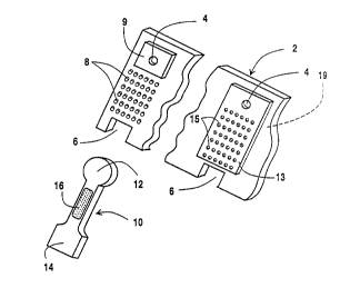
Referring to Figure la there is shown a base film 2 such as
PVC, which has a first opening 4, a second opening 6 in the form
of a slot and disposed between opening 4 and opening 6 is a
plurality of circular spaced apart shapes 8 of an expanded
insulating material. As stated above, the shapes could be any
polygonal shapes such as circles, squares, triangles, rectangles
or the like. To prevent inadvertent shorting of the test
component 10 to the cell housing, an insulating material 9 is
placed around opening 4. Preferably, insulating material could
be an expanded insulating material. Shown in Figure lb is a
second embodiment of the invention in which the expanded
insulating material is a solid material 13 having a plurality of
openings 15. A conductive layer 10 is selectively shaped so
that it can be placed over opening 4, opening 6 and at least
some of the plurality of expanded shapes 8 or openings 15.
Opening 4 is sufficiently large so that conductive segment layer
12 can be depressed into and through opening 4. Opening 6
is in the form of a notch so that conductive segment
layer 14 can be depressed into and through notch 6 to
contact a terminal of the cell. On top of conductive
layer 10 is a thermally sensitive material 16 such as a
thermochromic material, which will change color upon
detection of a particular temperature level. As shown
in Fig. 2, conductive layer 10 is shown secured on base
film 2 releasably secured to carrier layer 11, such as
a silicone web, and disposed over opening 4, opening 6
and the plurality of expanded shapes 8 of the first
embodiment of this invention. Disposed on top of
conductive layer 10 is thermally sensitive material 16.
If desired, a nonconductive film or coating (not shown?
could be disposed over base film 2 thereby further
'securing conductive layer 10 and thermally sensitive
material to base film 2. This top layer could have an
adhesive side to secure to the base film 2. This
nonconductive film could be in the form of a tube that
could be~heat shrink onto the cell after the label is
applied to the cell. Base film 2 has an adhesive layer
19 on its bottom surface (shown in Figure 1) which is
secured to a battery as shown in Figure 3.
Specifically, Figure 3 shows a battery test label 17 on
base film 2 (not shown) secured to the housing of
battery 20. Conductive segment layer 14 can be in
electrical contact With cover 22 which represents one
terminal of battery 20. This conductive segment layer
14 can be permanently connected to conductive cover 22.
The conductive segment layer 12 is disposed over
1 opening ~ and is spaced apart from the cylindrical
housing 24 of the battery 20 which is the second
terminal of the battery 20. Thus the circuit between
the two terminals of battery 20 via conductive segment
layers 12 and 14 is open. To close the circuit,
- m-
pressure is applied on the flexible upper layer above
opening 4 in the base film. The pressure will cause
the conductive segment layer 12 to make electrical
contact with the battery housing 24 through opening 4.
Rigidity and springback in the~label will cause
conductive segment layer Z2 to break contact with
housing 24 when the pressure is released. If desired,
conductive segment layer l4 can also be spaced apart
from the cover 22 so that to complete the circuit,
pressure will have~to be simultaneously applied to the
flexible upper layer above both openings 4 and 6 in the
base film. When the pressure is released, conductive
layer segments 12 and 14 will spring back and break
contact with the housing 24 and cover 22, respectively.
As stated above, suitable graphics and printed matter
can be placed on the base layer, conductive layer,
thermally sensitive material and/or the outer layer_
As shown in Figure 4, an outer layer 1 contains
designated areas 3 and 5 Which correspond to the first
terminal area and second terminal area, respectively,
of the cell. Designated area 7 exposes an area of the
thermally sensitive material so that When areas 3 and 5
are depressed, a circuit is completed and the thermally
sensitive material will change color to indicate the
state of charge of the cell. If desired, either area 5
or area 3 could be permanently secured to the second
terminal so that only area 3 or area 5, respectively,
would have to be depressed to complete the circuit.
This invention has been described in detail with
particular reference to preferred embodiments thereof,
but it will be understood that variations and
modifications can~be effected Within the spirit and
scope of the invention. For example, an adhesive strip
could be secured over the conductive circuit layer
- ~s- 2l~'?'~~~
containing the thermally sensitive material so that the
conductive circuit layer could be secured to the base
film using the adhesive strip.
x