Note: Descriptions are shown in the official language in which they were submitted.
wca ~~izoao~ ~d Pcriu~~zioz~46
Description
Determining Optical Signal Transit Delay
Time In An Optical Interfer~meter
Technical Field
This invention relates to optical interferometers and
more particularly to determining the optical propagation
(transit time) delay incurred by a signal traveling in a
fiber optic loop.
background Art
It is known in the art that a;sgecific type of optical
interferometer known as a fiber optic gyro (FOG) ~xses the
theory of relative motion to calculate the angular velocity
ar rotation rate of a body. A FOG typically consists of a
light source, an optical loop,,a beam splitter and
combines; a'phase modulator, and an optical detector:
Typica7~ly a light wave is infected into both ends of a
single fiber optic cable shaped in a circle (called a ring
or loop). The beam sputter serves to split the l~:ght wave
from the light source into two substantial~,y equal wages
~0 and sands them propagating in oPpos~.°te directions around
the optical loop. The lbeam combines serves to combine the
waves after they have traveled ~~eound the loop. and the
opticai detector measures the intensity ~f the combined
~ra~e-;-..:..,Tbe beam splzater and combines is typically one
component. Orae or more phase modulators, placed an one ar
both ends of the loop, may be used tc~ induce a phase shift
between thewavee.
When the optical ring is'at rest, i,a., not subject to
rotation, he two counter propagating light~waves, combined
SU~STITUT~ ~~iE~T
WO 9~/2040A PCT/US92/02746
~.d t 4
by the beam combiner and monitored by the optical detector,
will be exactly in phase because the distance traveled by
both waves is exactly the same. When the waves are in
phase, they combine for a maximum intensity at the optical
detector. When the ring is rotated about an axis normal to
the plane of the ring, the wave traveling in the direction
of rotation will recduire more time to reach the end ~f the
fiber (where the waves are combined), than the wave
traveling in the c~pp~site direction. This occurs because
the detector is moving away from,one wave and toward the
other. Therefore, the length ~f travel is shorter for one
wave than the other. This path difference causes a non-
reciprocal (differential) phase shift between the two waves
such that when the waves are combined, the optical
intensity is not a maximum: The phase shift induced Say the
angular rotation rate of the ring is known as the nSagnac"
effect.
For the purpose of closed loop, operation; as is known
in the art, such phase shift can be compensated for; i.e.;
nulled,'b~y imposing a phase shift on the waves equal and
opposite to the rotation induced (Sagnac) Phase shift such
tha,~ the phase difference between the waves,is brough'~ to
zero, restoring the maximum intensity at the optical
detector. The phase shift imposed ~o pr~duce the;desi~ed
null. in' closed hoop operation sereres as a measure o~
rotation rate and provides the game starting intensity for
each 'rogation rate thereby providing consistent sea~sia~.vity
to rotation rite measurement. There are various techniques
for imgosing this phase shift to null the Sagnac phase
SU~STITL'T~ ~~E~'
,., , ,,
.,4
,..
..: , , ;.::
.
,.
,...
:.f..:
,.4,..
.7.a,. .v., n..W. u.. ...,.. . .. ., n...... . ...... r .n.........f".. .....n
...... .....4.: ~.,......~: .. ...,.. o ,. . . ..
WO~ 93/2p4pg P~'/US92/02746
7
~. r.e ~.~ ~ ~> >
shift, one of which is a periodic ramp (also l~nown as a
sawtooth waveform, or serrodyne waveform) applied to
parallel electrode plates located around optical waveguides
at one or both ends of the optical loop. A voltage applied
to the plates induces a proportional phase shift in the
waves propagating between the plates. By controlling
either the amplitude or the frequency of the waveform one
can inaect various phase shifts at different times on tine
waves. For example, in a fixed amplitude serrodyne
modulation closed loop FOG, the change in serrodyne ramp
frequency needed to null the Sagnac phase is proportional
to the rotation rate of the ring.
In addition to using a serrodyne waveform to
counteract the rotatioxaally induced Sagnac phase
difference, a~technique is typically employed to increase
the sensitivity of the closed loop system to changes in
rotation. ~ne such technique utilizes the property that
the combined wave intensity behaves like ~ vertically
shifted (raised) Cosine curve (i.e., a curve with a non-
2~ zero average value having the negative-m~st point at zero),
where the intensify seen at the optical detector is
related, by this curve; to the phase difference induced by
rotation. When the ring is at rest, the combined wave
.,
intensity is at a maximum and thus the intensity is at the
pea3c of the cosine curve: However, at the peak, the
sensitivity is at a minimum because the slope is
effectively zero at this point. Therefore, any change in
phase shift will produce a minimal change in,intensity,
yielding minimal sensitivity. What is commonly done in the
SUBSTITUTE SHEET
wo ~~izo4os Pcrms~zioz~4~
art to increase sensitivity is to shift the operating
point, or the non-rotation null, from the maximum of the
c~sine curve to a region where the slope is much steeper,
i.e., at either ~r/2 or -~r/2. This can be accomplished by
applying a constant or DC phase shift (or DC sensitizing
source). However, if a DC phase shift is induced at ~r/2,
the steep slope of the cosine curve at ~/2 creates a high
sensitivity to phase changes recauiring a very stable and
accurate DC s~urce to avoid erroneau~ rotatioa~ rate
readings. It can be difficult to ach~.eve a very constant
DC phase 'shift over dime; and any change in this DC shift
will induce an incorrect indication ~f rotation rate.
Instead, systems .will typically modulate or change the
operating point in time from one side of the'cosine curve
where the intensity is most sensitive; t~ the ~ther side of
the cosi.ne curve where it is also most sensitive. This
modulation is hereinafter referred to a~ a sensitizing
oscillation (i.eo; AC'sensitizing). This is achieved by
dri~ring the modulator with a waveform such that the: phase
shift between the counter°propagating waves varies i.n a
kn~wn-way. If such a modulation source is used to improve
sensitivity; a demodulator is needed at the output of the
optical detector to detect signal components generated by
;,
rot~t~~n. Typica~:ly what is used is'a ynchronous
demodulator driva~n at the same frequency as the sensitizing
oscillator source (also knows as the fundamental
frequency). This is also referred to in the literature as
a lock--in amplifier. When a phase shift. ~dcurs, due to
rotation, components at the output of the .demodulator ,
~USSTBTUTE SHEET
Wp 93/20408 ~ ~ ~ ~ PCT/US92/0274~
- 5 -
change in a predictable way allowing the calculation of
rotation rate.
A typical closed loop fiber optic gyro will contain
both a sensitizing oscillator and a synchronous
.5 demodulator, as well as a sawtooth waveform driver placed
in a closed loop configuration. The sensitizing oscillator
and synchronous demodulator are provided for improved
sensitivitg~ and the sawtooth waveform generator is provided
to close the loop, e.go, to null any phase differences due
to rotation rates. Therefore, in a closed loop serrodyne
waveforan. FOB, both the sensitizing oscillatar and the
sawtooth waveform are simultaneously applied to the optical
phase modulator . For a given rotation rate there will
exist a corresponding frequency and amplitude of the
sawtooth waveform that will null the induced phase shift.
Although i~ is possible to drive the optical phase
modulator with a "zero" frecgtW ncy sawtooth waveform when
the ring is ~.t rest, it is known that using a non°zexo
frequency may be more practical: ~eh at rest them are
numerous ramp free~u~ncies, including zero, which will mull
the gyro output:- Lf the frequency selected is zero, the
non-rotating phase shift will remain at null independent of
variations in certain physical parameters of the FOG.
However, using "zero" frequency may be impractical because
it requires a very accurate reversal of ramp polarity when
the rotation directi~n reverses. If this accuracy is ndt
achieved, large err~rs may result. An alternative to ~xsing
"zero" frequency is to use one of the non-zero output
nul,ling frequencies when the gyro is at rest. However, the
SUSSTdTUTE SHEET
wp ~3izoaos PC'f/US92/02746 .
~;~:'~~:~ fl~~
allowable non-zero output hulling frequencies may drift as
physical parameters of the FOG change. This drift will
create a false indication of phase shift causing an
erroneous rotation rate indication thereby degrading the
accuracy in measuring FOG rotation rate.
More specifically, it is known that a FOG produces
accurate rotation measurements when the zero rotation
output hulling frequency is set to some integer multiple of
the loop.eigenfrequency, Fe. This frequency is defined as
to half the reciprocal of the 1~op delay time T and is related
to physical parameters of the system by the following
relationship:
Fe = 1/2T = C/2nL (1)
where C is the speed of light in a vacuum: n is the index
~f refraction for he loop optical medium; and L is the
length of the loop nptica~. fiber or waveguide: Equation 1
shows that the loap eigenfrec;uency (Fe) will change with
elzanges in e:~aher n or Le For example, a change in
temperature w~:ll cause a change in the length L of the
loop. Additionally; a change in temperature may cause a
change in the optical properties of the fiber and
therefore, a change in the fiber refractive index. These
changes in the ' fiber length and refractive index change the
;,
loop ttansit ime; and therefore, the loop eigenfrequency
(Fe).
In the c1~~ed loop fixed amplitude serr~dyne drive
FOG; when the ring ~;s at rest, the drive frequency (Fd) is
driven ~o the loop eigenfrequency (Fe) or a multiple
thereof, n~Fe, to achieve the nonrotation intensity
wc~ ~~izaao~ ~crius9zioa~a6
setpoint (null point). When the ring is subjected to a
rotation rate, closed loop control logic will force the
drive frequency to a new value to achieve the nonrotation
phase shift. This change in drive frequency is
proportional to rotation rate. This technique is accurate
provided the Fe in the control logic (with respect to which
the change is measured) matches the loop Fe of the FOG.
However, if the physical characterista.cs of the FOG change,
causing the loop Fe to change, there will be a
~t0 corresgonding intensity change that the contr~l logic will
compensate for by changing the drive frequency to maintain
the nonrotation intensity. This intensity change is
induced by the periodic modvxlation drive waveform acting on
the counter-propagating waves whose propagation time has
been changed by the change :in the ph~rsical characteristics.
Heoause the control logic is unaware of the loop Fe shift,
this change-in drive frequency will manifest itself as an
erroneous rotational reading.
It is also known in the art that, to achieve optimal
performances the fundamental frequency f~r'the sensitizing
oscillator and the synchronous demodulator can be set at
Fe. However, if the loop Fe drifts, this ~ptimal
performance will be compromised:
~,
Disclosure of Tnvention
Objacts of the invention include provisibn ~~
non~otating bptical transit time (propagation delay)
determination in a fiber optic gyro sensor employing cloyed
_ loop control which reduces the sensitivity to variations of
certain sensor parameters that would otherwise cause errors
SUSSTITUTE SHEET
Wa 9~/2040F~ ~ ~ ~ ~ ~~'3 ~ ~ PC:T/U~92/02746
g
in rotation rate indications and which permits the
determination of such transit time while the gyro is in
motion.
According to a first aspect of the present invention,
"on-line°' calibration of a Fc~G is achieved by switching the
amplitude of a component of the modulation waveform to a
value close to one for wh~.ch the time average of the
optical intensity will be a predetermined constant,
independent of rotation rate. To achieve this amplitude
more exactly, a synthesized rotation gate variat~,~n (phase
dither) is injected to the phase modulator in addition to
the other signals: This rotation variation is monitored
while varying the amplitude to achieve the exact amplitude
that provides iinsensiti.vity to this induced variation.
once this amplitude is reached, the sawtooth output
frequency ~f the closed to~p system provides the necessary
information to determine the optical transit time that
mould exist in the absence of rotation, ~,.e:, the transit
time ass~ciated with the current ~ralues of the physical
~0 parameters in the system: Once this nonrotation transit
time is kn~~an, the system sari be adjusted to compensate fc~r
it thereby minimizing the effects of varia~ion~ in this
' ;transit time
A'cc~rding o a second aspect of the invention, an
independent modulation wavef~rm is sa.mulaa~e~uslY applied
to the phase'modua.ator along with other normally applied
waveforans. This additioxaal waveform is driven at an
amplitude t~ provide insensitivity to rotation rate (as
hereinbefore described); and may also include a synthesised
SUBSTITUTE SH~E7"
CA 02122906 2000-08-24
64159-1261
_ g _
rotation rate variation for fine tuning the precise amplitude.
This technique provides a continuous output of optical transit
time in real time and avoids the overhead of switching
waveforms.
In accordance with the present invention, an optical
interferometer including an optical delay time determination
system, comprising: an optical waveguide loop; means for
providing a pair of light waves counter-propagating in said
loop; means for combining said light waves after counter-
propagating in said loop; detections means, responsive to said
combined light waves, for providing an electrical detection
signal having a component indicative of an optical phase
difference between said combined light waves, resulting from a
non-reciprocal motion applied to said loop, said component
having a time average; modulator means, disposed in said loop,
responsive to a drive signal, for inducing a phase difference
between said counter-propagating light waves; and signal
processing means, responsive to said detection signal, for
providing a drive signal to said modulator means having an
amplitude to induce a phase shift of ~ that causes the time
average of said component of said detection signal to equal a
constant magnitude independent of said non-reciprocal motion,
thereby maintaining said constant magnitude time average of
said component at a value which would exist in the absence of
said non-reciprocal motion, and for interactively adjusting the
frequency of said drive signal to achieve said constant
magnitude time average of said component of said detection
signal, so that said adjusted frequency equals a non-rotational
setpoint frequency.
A further advantage of the present invention is that
if the system employs an AC sensitizing oscillator and the
oscillator uses the loop eigenfrequency Fe (which is directly
related to the loop transit time) to derive its fundamental
CA 02122906 2000-08-24
64159-1261
- 9a -
frequency, knowing the loop Fe will allow adjustment of the
fundamental frequency for the sensitizing oscillator and the
demodulator, allowing these devices to track variations in the
loop transit time, thereby maintaining optimal system
peformance.
The invention may be implemented in a system
employing a closed loop rotation control with AC or DC
sensitizing, or no sensitizing.
The foregoing and other objects, features, and
advantages of the present invention will become more apparent
in the light of the following detailed description of exemplary
embodiments thereof, as illustrated in the accompanying
drawings.
Brief Description of the Drawings
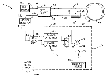
Fig. 1 is a schematic block diagram of an
interferometric optical sensor having amplitude switching in a
closed loop serrodyne drive configuration in accordance with a
first aspect of the invention.
Fig. 2 is a diagram illustrating the phase shift
imposed on two counter-propagating waves, the phase difference
between the two, how this phase difference
wo ~~izoaas ,.~ ,~:,~:~ ~'~ ~ ~crius~2ioz~a~
-- 10 -
appears on an optical intensity curve, and the associated
time history of the optical intensity.
Fig. 3 is a graph of a family of curves representing
the serrodyne output drive frequency as a function of both
serrodyne output drive amplitude and rotation rate.
~'ig. 4 is a schematic block diagram of an
interferometric optical sensor having multiple simultaneous
serrodyne waveforms applied and controlled in accordance
With a second aspect of the invention.
Best l~Iode For Carrying Out The invention
Referring to Fa.g. l; a closed loop i~terferometric
optical sensor, more specif'.cally a fiber optic gyroscope
(FOG) 10, includes a light :source 12, e.g., a laser diode
or superluminescent diode. Light from the source 12 is
optically coupled by known means, e.g., through an optical
fiber 14 to a port 16 of an optidal assembly 18.
The optical assembly 18 contains known optical
components such as beam splatters (e. g.; four port fused-
fiber star coupler or integrated optical Y-coupler);
polarizers, and single-mode elements (e.g., singl:e-m~de
fibers or waveguides). The components are arranged such
that ligh~~ which has entered at port 16 is first passed
through a single-mode single-polarization filter, e.g.; a
kno~an...inetallized' optical waveguide- segment; then split 'by
kno~rn means; e.g.; a Y-shaped integrated'optical (IO)
waveguide, into two waves ~f approximately equal-..
intensities which then exit from the assembly 18 through
:two ports ~0, 22.
SUSST1TUT~ SHE~!'°
wa ~m2oaot~ ~cr~us9zioz~46
~.~ ~ ~ i s~ ~~ r~ t~~
F~a rf F:~ ,i E,f i.i
- 11 -
The port 22 is optically coupled by known means, e.g.,
through an optical fiber 24 to a port 26, of a phase
modulator assembly 28, which may alternatively be part of
the optical assembly 18. An optical wave entering port 26
is directed through optical fibers or waveguides, to an
optical phase modulator 30. The modulator 30 may include,
an optical waveguide sandwiched between a pair of parallel
electrodes by known t~chnic~ues. The modulator 30 is driven
by a modulation signal on a line 32 from a modulation
control circuit 34. After passing,through the modulator
30, the wave exits the modulator assembly 28 thr~ugh a port
36. The port 36 of the modulator assembly 28 and the port
of the optical assembly are optically-coupled thrbugh ,.
optical fibers 38, 40 respectively to opposite ends of an
15 optacal fiber 44 wound into a Sagnac sensing loop. The
fiber 44 typ~.cally consists of a single-mode fiber, but may
be a multi~m~de fxb~r if desired. The loop may consist of
. a plurality of burns of optical (fiber which may be wound on
a cylindrical sp~ol dr~ot shown). The two waves, one
20 exiting the port 20 of tl~e optical assembly and the other
exiting the port 36 of the phase'modulator assembly
counterpropcgate in the loop.
After trave~sinc~ the loop; the wave that exited,~he
port 20~enters tie modulator assembly at the port 36;
passes through the modulator 30 and re-enters the optical
assemble at the p~rt 22. The other wwe, after traversing
the 1~0~; re°~enters the opt~.cal assembly~at the port 20.
-Tra'the optical assembly l8, the waves are recombined by
known means, e.g.; the aforemewtionad 'Y-shaped 10
SUBSTITUTE SHEET
wp ~~izoap~ ~ ,;~ ~ ~ ~ r ~ PC:T/US9~/02746
- 12 --
waveguides. A portion of the recombined light is split off
by known means, e.g., a fused-fiber coupler, after again
passing through the aforementioned single-mode single-
polarization filter to ensure, as is known, reciprocal
optical paths for the counter-propagating waves in the FOG
in the absence of rotation.
The split-off portion of the recombined light exits
the optical assembly through a port 48 and is optically
coupled by known means, a:g., an optical fiber 50, to an
optical detector 52, e.g., a photodi.ode or ph.otodetector.
The remainder of the recombined light (none of which
matters to the invention) typically exits the optical
assembly 18 through the port 1:6', and may pass though cr be
absorbed in the light source 12.
The optical. detector 52 provides on a'line 54', to the
modulation control circuit 34, an electrical signal
proportional to the intensity of the optical signal at the
port 48 of the optical assembly I8. This optical signal
represents the recombined'waveform a.nteneity.
During FOG operation the modulation control circuit 3,4
monitors the optical intensity on the lies 5~ and drives
the optical phase modulator with a modulation signal on the
fine 3 2
As~is known in tk~e art, the closed loop FOG modulation
ei~n~l may be a stepped ramp or a linear ramp serrodyne
signal having a fixed amplit~xde (or peak) and an
essentially instantaneous flyback time:- The terms 2~ and ~r
radians amplitude refer to the amplitude required to induce
a peak phase shift of 2~ and ~r radians, respectively on a
SUBSTITUTE SHEET
WU 9:3/204(IH ~ ~ ~i ~ ~ ~ ~ PCT/US92/02746
- 13 -
given wave. Typically, a 2~r radians amplitude is used in a
fixed amplitude FOG. The phase modulator induces a phase
difference between counter--propagating waves because it
acts on the recombining waves at different times.
The modulation control circuit of the invention
includes a known frequency control circuit 56, that
provides an analog serrodyne waveform drive signal on a
line 58 responsive to the optical intensity signal on the
lane 54. The frequency control ca:rcuit modulates the
frequency from a nonrotation setpoant frequency (or control
Fe) to nul l any induced dif~e~ential phase shift and .
maintain a constant intensity averaged over the period of
the serrodyne drive signal. The frequency control circuit
contains known electronic compon~nt~s such as a lock-in
amplifier (synchronous demodulator); providing an analog
voltage proportional to the magnitude of frequency
components in the intensity signal, driving a low pa~s-
fil er; providing ~ vol age indicative of the time averaged
intensity of the frequency components, which drives a
' volaage ,controlled oscillator (VCO) to provide a frequency
proportional to the time averaged 'i~ntensit~e
The serrodyne drive signal is provided from the
frequency control circuit ora the line 58 to a knewn 2~r
i
amplitude control circuit 62 where it is scaled to a fixed
amplitude of approximately 2~ radians using known
elee~ronic components, e:g:, an amplifier.
den FOG 'calibration is not selected (i.e. normal FOG
operation), the frequency control circuit 56 provides a
sighal on a line 64 ~o cause a swiach 68 to connect the 2~
~U~STITUTc SH~~T
w~ ~~izoaoR y ~ ~ ~ ~ '~ ~~ PCT/U592/027a6 ,
- 14 -
amplitude control circuit 62 to a line 70 which feeds one
input of a summer 72 and causes a switch 74 to disconnect
the signal path to the other input line 78 of the summer 72
thereby providing a modulation drive signal on the line 32
solely dra.ven by the signal on the line 70. In this mode
of operation the serrodyne drive signal frecyuency on the
line 70 will be related to potation rate. More
specifically, the difference between the drive frequency
and the nonrotation setpoint frequency (the control Fe)
will be proportional to rotation rate. A signal indicative
thereof is provided by the frequency control circuit 56 on
a line 76 which is the F~G l0 output.
The serrodyne waveform drive signal on the l~.ne 58 ~.s
also provided tc~ a ~ amplitude control circuit 80
containing known electronic do~ponents such as a frequency
t~ voltage converterwwhich controls the gain of a variable
gain amplifier: The ~r amplitude con~.rol circuit scales the
amplitude of the serrodyne drive signal on the line 58 to
approximately r~ radians, ,detects freguez~cy variations in
the s~rrodyne e~rive signal, and adjusts the amplitude' to
minimize such variations thereby achieving precisely a n
radians amplitude. T have f~und, both analytically and
experimentally, that if the serrodyne amplitude is
preci.~s~ly equal to ~r radians, the closed loop outpaat drive
frequency is precisely equal t~ the loop Fe (or an odd
multiple thereof) independent of F~G rotation rate.
FOG calibration is selected by the output of a timer
located within the frequency control circuit 56. At a
predetermined rate such as once per minute, the timer
SUSSTITUT~ ~H~ET
Wp 9~/~p~p~ ø~ ~ ~ P~'/US92/02746
15 _
initiates calibration by causing the frequency control
circuit 56 to provide a signal on the line 64 to cause the
switch f>8 to connect the sr amplitude control circuit 80 to
the line 70 which feeds the summer 72 and causes the switch
74 to connect an undulation source 82 to the other input
line 78 of the summer 72 thereby providing a modulation
drive signal on the line 32 which is the summati.Qn of the
signals on'the two lines 70, 78. The undulation signal
from the source 82 ~rovieles on the line 78 a predetermined
artificial rotation (phase) variation signal such as a low
frequency dither, e~g., lH~, as a component to the phase
modulation drive signal. The dither manifests itself as a
variation in drive signal frequency on the output line 58
~f the frequency control circuit 5f. The ~r amplitude
~.5 control circuit will adjust the amplitude in a da.rection to
minimize the variati~n in drive frequency. in7~en the
frequency variation is extremely small or nonexistent
(prcwided the ~.nop Fe does not change), the amplitude ~f
the signal is precisely ~r radians. Thus, are iterative
pr~cess exists vrhereby the frequency control eircuit'
modulates the drive frequency to achieve the nanrdtation'
se~point and the ~r amplitude control circuit adjusts the
drive amplitude to achieve predisely ~r radians amplitude:
i~hen both the drive frequency is equal to the 1~op Fe and
the-drive amplitude equal's ~ radians, the drive frequency
will be independent of rotation rate thereby allowing
determination of the loop F~ by monit~xing the drive
f r~quency s
~U6ST1T~1TE S~~FT
gyp 9~/2p4pA ~ ~ ~ PC'~'/US92/02746 ,
- 16 -
After waiting a length of time sufficient to achieve
the n radians amplitude, such as three periods of the
undulation frequency (three seconds, for an undulation
frequency of 1HZ), the frequency control circuit reads the
drive frequency signal on the line 70 (which will xaow be
equal to the loop Fe) and updates the value of the control
Fe (which will update the rotation rate). t3pdating the
rotation rate calculation may also be performed with~ut
modifying the contxol Fe. After updating the control Fe
20 value, the frequency control circuit disengages the FOG
calibration by providing a signal on the line 64 to cause
the switch 74 to disconnect the undulation source 82, and
cause the switch 68 to connect the 2~r amplitude control
circuit to the summer 72 and disconnect the n radians
amplitude control circuit. The system has thereby returned
t~ the 2~r amplitude closed lc~p conf~.gu~ation and is
capable of m~asuri.ng rotation rate.
Referring nc~w to Fig. 2, when the driving amplitude is
~ radians the optical intensity'seen by the detector on a
time average basis will be a cohstant, independent of
rotation rate. The waveforn~s lOn; 202 illustrate' the ~r
radians ampl,itud'e serrodyne wavef~rm and the associated
phase shift co introduced on the counterclockwise (CCW) and
clockwise ('CW) traveling waves, respectively: The time T
represents the time it takes for the wave tea traverse the
loop:
The-phase ~h~.f~ introduced between the two waves (l~~)
can-,be determined by subtracting the two waveforms as shown
by the curve 1:04. This curve 1.04 shows the differential
~~~STITUTE SHEET
PCT/US92/02746
w~ ~~izoan~
_ 17 _
phase shift introduced between the two waves to be +~/2 and
-~r/2 with equal times at each level. The effect of the
differential phase shift ~a~ (curve 104) upon the intensity
I of the optical output signal is shown by the raised
cosine curve 106.
For eacample, given a nonrotating operating point 108
at the top of the cosine curve 106, if the differential
phase shift shown by the curve 104 is imposed on the waves,
the intensity will osc~.llate:~rom the pointll0 to the
point 112 in a periodic fashion spending equal tames at
each intensity. The time average output intensity in this
case is equal to a constant, corresponding to a ~s~ of ~/2,
shown by the curve 114. If the ring is then subject to an
arbitrary rotation rate, the operating point on the
intensity curve wily shift tra a related point, such as 3.16.
Again; applying the differential phase shift 104 to the
cosine intensity curve 106; the inten~~.ty will oscillate by
~r/2 from the operating point'116 to two new points 11$,
'120, again with equal times spent at'ea~h intensity. The
curve 122 shsws the time history of the intensity
oscillation at the operating point 116. The time average
intensity 114 is equal to the same constant value as ~n the
.previous case, independent of rotation rate. Therefore,
the time average intensity seen at the optical detector
will be the same constant value, independent of rotation
rate, when the serrodyne waveform amplitude is set to
precisely ~r radians and the fre~ency in set to Fe. It
should be noted that the time delay induced by rotation is
many orders of magnitude smaller than the tame T to
SUTITUTE SHEET
wo ~~i2o4o~ ~ :! ~ ~ s~l ~) ~>
PC.T/US92/02746 .
18 -
traverse the loop, therefore no appreciable change in the
time symmetry of the ~1~ waveform 104 will occur due to
rotation.
This principle is further illustrated by Fig. 3. The
x~-axis 130 and y~-axis 132 represent the amplitude and the
frequency of the serrodyne output drive signal
rerSpeCit~.vely v For a given rotat~.on rate and ampll.tude of
the serrodyne drive signal, the y-axis of Fig. 3 gives the
closed loop serrodyne drive output frequency required to
null any induced phase shift and obtain a constant optical
intensity averaged over the period of the serrodyne drive
signal (i.e., the frequency of the signal on the output
line 58 of the frequency c~wtrol circuit). The Family of
curves 134 ill.u~trates the r~elatibnship for CC~1 rotation,
curves 13~ for CW rotation, and curve 13~ for no r~tation.
.fit the normal 2n radians fixed amplitude operating
condition,;the change in frequency required to satisfy tl~e
closed loop serrodyne drive system is prop~rtional tn
rotation rate, as indicated by the family of curves 134,,
136, 138. However,, when the amplitude used i.n ~r rada.ans, ,
the frequency at which this occurs is one unique frequency,
Fe, as shown by the intersection of all the curves at the
'point 140.
Although the invention is illustrated .in Fig. 1 as
being imp3.emented with a switched waveform, the invention
will work equally as well uszng two independent serrodyne
modulation waveforms with amplitudes ~r and 2~
simultaneously applied to the phase modulator and
contrr~lled such that one frequency gives the loop Fe, and
SUBSTITUTE SHEET
WC193/2040~ ~ g r ,~ PCT/US92/02746
~~:.'~a~:~3~
- 19 -
the other contains rotation information, as illustrated in
Fig. 4. Tn this configuration, the value of the loop Fe is
available continuously on the line 70 and rotation
information on a line 86. The use of simultaneous
waveforms in this alternative embodiment eliminates the
switch 68 that selects between the rr and 2~r amplitudes, and
the switch 74 that connects the undulation signal. The 2~r
amplitude signal on a line 86, the ~r amplitude signal on
the line 70, and the undu7.ation signal on a line ~0 are fed
to a summer 88 that replaces the summer 72 of Fig. 1,
thereby continuously providing a drive signal on the line
32 comprising three-combined waveforms.
To allow the simultaneous signals to be distin~u.ished
and minimize signal interaction in this alternative
embodiment, the frequency control circuit for the ar and 2~
radians amplitudes should be based at different frequencies
(such as ~r radians amplitude at Fe and 2~r radians amplitude
at 2Fe). Accordingly; the frequency control circuit in
this embodiment produces two serrodyne waveform signals
based at two dif~er~nt frequencies. An output line 59
provides a path fir the'addi~ioraal signal. The use of
simultaneous wavefo~ns in this alternative embodiment
eliminates the overhead associated with=switching from the
2~r radi'ans amplitude c~ntr~l: circuit to the ~r radians
amplitude ~c~ntrol dircuit and undulation source, thereby
eliminating the interruption in rotation rate detection
during the time when the sr radians amplitude is applied.
It is known that using a sensitizing oscillator and a
synchronous demodulator both driven at Fe as their
SUBSTITUTE SHEEN'
Wt) 9:i/2Q408 G ~ ~ ~ ~ ~ ~~ PCT/US92/02746
20 -
fundamental frequency, allows the FOG to exhibit optimal
performance by reducing errors such as those resulting from
optical backscatter and from spurious intensity
modulations. It should be noted that a sensitizing
oscillator and synchronous demodulator away be used with the
present invention. Therefore, systems employing a
sensitizing oscillator and synchronous demodulator may use
the present invention to maintain optimal performance by
adjust.ng the fundamental frequency to track any changes in
the loop Fe.
although the invention is illustrated primaril~r as
applied to a rotation sensor, it will work equally as well
in applications where optical phase diff~rence~ between
counter-propagating waves in the loop ace induced by
alternative perturbations, e.g., magnetic fields configured
s~ as to yield a differential phase shat; rather than
rotation. FurthexTnore, although the controlled modulation
signal is illustrated as being a seer~dyne ramp signal
other wavef~rms exhibiting similar phase shifting
properties tsetry) may be used, e:g, a parabolic
periodic ramp or any non;-linear periodic ramp with a
flyb~ck time that is sh~rt compared to the forward ramp;
v time, and with an aPProPriate amplitude:
~.~,Tn additi~n; although the invention is illustrated as
comprising in past an aptical assembly which may provide
~ptica~. splitting; filtera.ng; and combining opemtions;
along t~aith a separate modulator av~er~bly,' the invention
will work equally as well when implemented with the
indivic~u~1 componen°~s combined in one or more IO devices,
~IBSTdTUT~ SHEET
~~ ~ %~~ ~ ~~ f"~ ~' PC"~'/L~S92/a2746
w~ ~:~/xoa~~ ~,~ :~ w~ W ;~~ c~ t
- 21 -
in a manner which should be apparent to one skilled in the
art in light of the teachings herein.
Tnstead of using an undulation (or dither) source to
fine tune the ~r amplitude, the invention may employ an open
. 5 loop amplitude control without both the undulation source
and ~r amplitude control logic, provided the ~r radians
amplitude is precisely known. Alternatively, if the gyre
or other target application has a known inherent mechanical
dither similar to that induced by the undulation source;
the undulat~.~n source is not required.
Furthermore, even th~ugh the invention is described as
using only one phase modulator and one drive signal, it
should be understood ~hatythe invention may also be
implemented with a plurality of phase modulators driven by
separate signals,'one for each signal cnmpon~nt (or a
combinati~n thereof) previ~usly described as summed or
switched into the modulator elriv~ signal. In this
configuration, the linearity of the optical system allows
the indiv~,dual effects of each drive signal to be optically
2~ combined, thereby forming the total modulation signal.
instead of being implemented:'in dedicated'h~rdware as
described with'respect to Figs. 1 arid 4, all of-the
functions of the present invent~.on relating to the ,
modulation control circuit 34 ~:n Figs. 1 and 4, may be
implemented in software by suit~bie programming of a
digital computer.:
Although the invention has been described and
illustrated with respect to certain exemplary embodiments
thereof, 3t should b~ understood by those skilled in the
~U~~TITUTE SHEE'f'v
WO 9~/2t)4OA CPC 1'/L~S92/02746
~:~ ~'~'~?~~~
- 2 2 ~-
art that various changes, omissions and additions may be
made without departing from the spirit and the scope of the
inventionv