Note: Descriptions are shown in the official language in which they were submitted.
~, WO93/10477 PCTJUS92/09707
x 2123310
,,, 1
,,~.,
~ .
,,,
.' CHIRAL SMECTIC LIQUID CRYSTAL
OPTICAL MODULATORS
",
1"
; ~
,~ Field of the_Invention
The present invention relates to tunable electro-
optical modulators having a folded optical path structure
using chiral smectic li~uid crystal materials as tuning
~ elements and, in particular, relates to Fabry~Perot
j~ intererometer and etalon modulators.
~0 Backaround o~ the Invention
Liquid crystal devices operate on the basic principle
. that due to the dielectric a~isotropy vf nematic,
cholesteric and smectic:~ liquid ~cry~itals, the average
molecular axis, ~r director, can be oriented in the
presence of an~ applied electric field. The coupling of
non-ferroelectrlc ~i~uid crystals to the applied field is
a weak, sscond~order interactionO In general, slow
: r~sponse~ti~es::are~charac~eristic oP non-ferroelectric,
non~chiral,~liqu~d~crys~al optical devices.
~ ~eyer et al~ 'Ferroele tric ~iquid Crystal~9', in Le
Journai de Physique, V~ 36, March, 1975~ pp. L69 L71)
howed that chiral:C or H~, smectic liquid crystals, could
be~ferroelectric~, tha~ is, possess a permanent electric
dîpoIe: density, P. ~This permanent polarization, P, is
~:;25: ~ perpendicul2r to the average orien~ation of the long axis
of the molecules ~denoted by the molecular director, n,)
and generalIy contained within a plane parallel to th~
smectic layers. In these chiral smectic liquid crystals
~(CSLCs), the molecular director makes a temperature
~'~
WO93/10477 PCT/US92/09707
2123310
dependent angle, ~, with respect to the layer normal, z as
shown in Figures 1 and 2. In general, ~ ranges from 0 to
45. The presence of the eiectric dipole provides a much
stronger coupling to the applied electric field as compared
to non-ferroelectric liquid crystals. Furthermore, the
coupling, and hence aligning torque is ab~ut linear with
applied field. The significance of this is that changing
the sign of the applied electric field will change the
direction of P in smectic C , H~, A~ and other chiral smectic
phase liq~id crystals.
N. A. Clark et al. in U.S. Patent No. 4,367,924,
realized a ferroelectric liquid crystal switching device ~y
sandwiching a thin layer o~ a smectic C~ ~SmC~) liquid
crystal between two glass plates coated with transparent
electrodes. In this patent, they describe the surface-
stabilized ferroelectric liquid crystal (SSFLC) device,
~;1 which employs SmC~ or SmH~ liquid crystal phases in the so-
called bookshelf geometry, otherwise designated the planar
alignment, where the smectic layers are perpendicular to
and the liquid crystal molecules are parallsl to the glass
,l plates which also contain the electrodes, as illustrated in
~.l Figure 1 (see also N. A. Clark et al. U.S. Patent 4,563,059
`l and N.A. Clark and S.T. Lagerwall in Applied Phys. Letts.
(1980) 36:899 and S.T. Lagerwall and I.Dahl Mol. Cryst.
1 25 Liq. Cryst. ~1984) 114:151-187). 55FLC SmC materials have
¦ been shown to be useful in a number of electro-optic device
applications including switches, shutters, displays and
spatial light modulators (SLM's). The advantagec of planar
aligned ~hiral sme~tic C,F,G,H, and I l~iquid crys~al
devices i~ their ne~rly three orders of magnitude increase
.i in swit~hing speeds over non chiral liquid crystal devices
. and their intrinsic bistability, which has applications for
, optical me.mory~units,
Tristable switching of a planar-aligned CSLC cell has
been reported (I. Nishiyama et al. (1989) Jpn. J. App. Phy.
~:~ 28:L2248; and A.D.I. Chandani et al. (1988) Jpn. J. App.
Phy. 27:L729). The third state of such tristable cells has
. I .
~ ~ .
WOg3/1~77 PCT/US92/~7~7
2 1~310
been linked with the presence of an antiferroelectric
phase, designated SmCA;. This type of CSLC cell has been
designated an antiferroelectric LC cell. CSLC materials
which aan exhibit this antiferroelectric effect have been
report~d by K. Furukawa et al. (1988) Ferroelectrics B5:63;
M. Johno et al. (1989) Jpn. J. App. Phy. 28:~119 and Y.
Suzu~i et al. (1989) Liq. Cryst. 6:167~
Lagerwall et al. in U.S. Patent No. 4,838,663,
de~cribe a non-tilted, non-ferroelectric, chiral smectic A~
(SmA ) liquid crystal electro-optic switch. With planar-
aligned, surface-stabilized SmA material between substrate
walls with no electric field applied (zero field state), n
I is parallel to z (i.e., ~ = 0). The molecular director of
the SmA material exhibits rotation in a plane relative to z
(~ ~ 0) in response to an applied electric field due to
the electroclinic e~fect tfirst described by S. Garaff and
R. B. Meyer (1977) Phys. Rev. Letts. 38:84B)~ These cells
display an analog dependence of ~ with applied field to a
maximum tilt angle ~x~ which angle is an intrinsic property
of the SmA material~ Materials having ~ ranging from
about 6 to 22.5 have be@n observed (see also, Sharp, G.
D. et al., (Opt. Lett:. 15) (199~) pp. 523-525). The
advantage of these planar-aligned SmA~ cells is
submicrosecond switchi~g cpeeds and analog rotation of the
2S optic axis. ~ ~
~' L.A: Beresne~et al. t European Patent Application No.
3 309774, published 1989, has recently described a new type
i of chiral smectic~ferroelectric liquid crystal cell called
the distorted helix~ferroelectric (DHF), li~uid crystal
c~ This type of device is similar to the planar-aligned
'1 chiral SmA device of Lagerwall et al., except that it is
j
not strongly surface-stabilized, so that the helix along
~! the direction of the layer normal, z is not suppressed.
ll Application of an applied electric field to the DHF cell
perpendicular to z, partially orients the molecular
directors by an angle ~ to z. The angle ~ is dependent on
i the size and magnitude of the field so the DHF device
" ,
WOg3/1~77 PCT/US92/0~707
2123310
operates in an analog mode similar to a Sm~ device. In a
DHF device there is a change in the birefringence o~ the
material as the molecules align, which does not occur in
Z~ either the SSFLC Sm~ or planar-aligned SmA device. The
~ 5 DHF materials, such as Hoffmann-La Roche DHF 6300, having
', ~x as large as ~37 have been described. The advantage of
DHF switching de~ices over other FLC switching devices
, described above i~ the variable birefringence with applied
~l~ voltage. This is similar to the operation of nematic
'i 10 li~uid crystals, which also yield a variable birefri~gence
~¦ with applied voltage. In contrast to nematic liquid
crystals, the DHF molecular directors rotate by their full
tilt angle within 40 ~sec, a significant advantage.
' Furthermore, the voItages required to rotate the optic axis
~; 15 are generally much lower than those required for SmA~ and
SmC cells. An interesting feature of DHF devices is the
coupling of the change in birefringence with the rotation
~,, of the optic axis as a function of applied voltage.
Z.M. Brodzeli et al.~(l990) Technical Digest on SLM's
and ~heir Applications 14:128 have reported fast electro-
optic response (20 ~:sec) in a homeotropically-aligned Sm~
liquid crystal. In homeotropic alignment, the smectic
layers of the liquid crystal are parallel to the surfa~res
of the substrate~ ~alls (se~e Figure 2) and as in planar-
~, 25 aligned CSLCs, the molecular director makes an angle, ~,
with the layer~normal. In the optical modulator described
,~
by Brodzeli~;et~ al./ th homeotropically-aligned SmC~
material is~ positioned between substrate walls having
deposited electrodes: (the width of the cell was given as 17
~m.) Polarized non-monochromatic light entering the
device, propagati~g~along the axis normal to the layers,
was~reported to be modulated in intensity by application of
a voltage a~ross the~electrodes.
Phase modulation of optical signals is often
;35~ accomplished by means of an electro-optic effect in which
a change in index~of refra~tion of a suitable material is
achieved with the application of an electric field, for
.~`( ' .
WO93/10477 PCTlUS92J09707
21233I O
example, by the Pockels or Kerr effect (see, e.g., Yariv,
A. and Yeh, P. Optical Waves in Crystals (1984) Wiley and
Sons, NY~. While the Pockel's and Kerr effects are high
speed effects, they require large voltages for bulk
S implementations in order to achieve very small electro-
optic effects~ A techni~ue that has been used to improve
the characteristics of electro-optic Pockel's and Kerr
effect phase modulators, is to fold the optical path l~ngth
using a Fabry-Perot etalon or resonator, which transt`orms
the low amplitude input signal ~o an output optical
intensity with high contrast.
A Fabry-Perot device consists of two plane parallel,
highly reflecting surfaces, or mirrors, separa~ed ~y a
distance, L. When the mirrors are fixed at distance L, the
device is called an etalon. When L can be varied the
device is called an interferometer~ ~ Fabry-Perot etalon
operates on the principle of multiple interference of the
waves reflected or transmitted by the mirrors. If L is a
', multiple of ~, then the transmitted waves destructively
, 20 interfere and the light incident upon the device is ideally
l totaliy reflected by thP etalon. If L is a multiple of 2~
j all the light is: ideally transmitted by the etalon
! (assuming no absorption losses)~ If the etalon thickness
is som~where in between ~ and 2~, then partial tran mission
1 25 or reflection occurs. If the optical thickness of the
I etalon can be changed, the etalon operates as a variable
modulator.
~' Miller:et al., U.S. Patent No. 4,790,643, disclose an
5, .optically bîstable device comprising a Fabry-Perot etalon
containing an intracavity, optically non-linear, nematic
uid crystal material. The device provides an eleckr~-
optic bistable switch tha~ is designed to modulate a
mosnochrom5atic or coherent light source. Since the liquid
crystal of this device is neither chiral or ferroPlectric,
the switching spseed of this particular optical modulator is
relatively slow.
5~ .
`,~ WO g3/10477 , PCr/USg2/09707
2123310
~; 6
Summar~ of the Invention
The present invention provides optical modulators
which comprise folded optical path structures, etalons and
interferometers containing chiral smectic liquid crystal
materials within the optical cavity which function for
optical modulation by an application of an electric field.
~ The intensity, phase and wavelength modulators provided
t'' herein combine modest voltage requirements and low power
consumption with rapid tuning . The device configurations
of the present invention permit discrete or continuous
optical modulation useful in a wide variety of applications
including, among others, spectrometry, remote sensing,
discrete modulation for differential absorption or
transmission in optical filters, rapid wavelength
;1 15 modulation useful in color displays, intensity modulation
for binary or gray-scale generation for shutters and SLMs,
phase modulation~for 2-D and 3-D holographic displays,
SLMs, beam steering, refractive and diffractive optical
elements. Folded optical~path structures include optical
modulators having~Fabry-Perot (FP) interferometer and
etalon structures and~ asymmetric Fabry-Perot cavities
i.e., Gires-Tournois etalons). The modulator
~ configurations~of~;the present invention are useful in
i~ single and multiple pixel elements which are electronically
or optically~addressable by a variety of means.
Most~ generally, this invention involves the
positioning~of~an~aligned Iayer of a chiral smectic liquid
,. .
crystal material within an optical resonance cavity. As is
~i conventional, ~an optical cavity is formed by opposed
~j 30 reflective surfaces. Preferably the reflective surfaces
are such that;a~substantial portion of the light entering
the cavity makes more than one pass through the cavity,
i.e., having at ~least one reflection, before exiting the
cavity. In a FP~etalon or interferometer configuration, it
~35 is preferred ;that~interference between at least two phase
retarded waves of light occur before light exits the
cavity. In an asymmetric FP configuration, folding the
~1
WO93/10477 2 1 2 3 3 1 0 PC~/US92/09707
optical path increases the interaction length of light
within the modulator. Typically, the reflective surfaces
are plane parallel with respect to one another and at least
one of the reflective surfaces is transmissive to allow
entrance of light into the cavity. FP cavities can be
operated in transmission/reflection- or reflection-only
mode with the choice dependent on the modulation
application and/or design requirements- The chiral smectic
liquid crystal material is aligned between substrate walls.
The ahiral smectic liquid crystal material can be planar-
or homeotropically-aligned. Means for achieving the
decired alignment, such as appropriate alignment layers, as
is known in the art, can be provided on the inside surfaces
..
of the substrate walls in contact with the chiral smectic
¦ 15 liquid crystal material. Means for applying an electric
field across the aligned material are provided such that
molecular director of the material, i.e., optic axis, is
rotatable on application of the electric field across the
material. A dc or ac electric field, or both, may be
applied to tbe cell to rotate the optic axis. In certain
device configurations with E applied parallel to the
smectic layers (i.e.~, E~is perpendicular to z), the optic
j axis is rotatable in a plane perpendicular to the direction
1 of the applied~field. The aligned chiral smectic liquid
crystal material,~substrate walls and means for application
of an el~ctric field~across the liquid crystal comprise a
~hiral smectic liquid crystal cell. Light traversing the
FP cavity containing~a chiral smectic liquid crystal cell
is modulated by~rotation of the optic axis of the cell by
`1 30 application of an electric field. The modulators of the
¦~ present invention optionally include i~otropic spacer
elements, lenses~,~ birefringent elements and wave plates
within the etalon cavity.;
This invention ~specifically provides tunable optical
~35 modulators of ;elliptically polarized light. Certain
optical modula~tor configurations herein are particularly
useful with linearly polarized light. The optical
.
.~ .
WOg3/l0477 PCTtUS92/09707
212~310
modulators of these specific embodiments do not require
exit polarizer means or polarization analy~ers to obtain
the desired modulation. It may, however, be desired, in a
particular application, to employ a polarization analyzer
to ~elect a certain polarization state of modulated light.
FP-type interferometer and etalon configurations of the
present invention, include binary and analog intensity,
phase and wavelength modulation. The modulators of the
present invention are optiaally or electronically
addres~able in single pixels or arrays of multiple pixels.
The i~v~ntion also specifica}ly provides tunable
optical modulators of elliptically polarized light which
comprise asymmetric FP cavities wherein the optical cavity
contains an intracavity modulator element positioned
, 15 between means for reflecting lighk entering the cavity.
~he light reflecting means in these modulators comprise one
reflective surface ha~ing si~nificantly higher re~lectivity
tha~ the other reflecti~e surface, ideally 1, such that the
device operates in the reflection-only mode. Both planar-
i 20 and hom~otropically-aligned materials can be employed as
1 the modulator element and appropriate alignment means are
optionally c~mprised within the CS~C cellO These specific
embodim~nts do not require the use of a polarizer to detect
~, optical modulation. The asymmetric FP etalon modulatoxs of
¦ 25 the present~ invention inalude binary and analog phase
modulatore.
~ Chiral smectic liquid crystal materials useful in the
:~ rapidly tunable~ or: switchable modulators of the pres~nt
invention include ferroelectric liquid crystal materials,
electFoclinic li~uid crystal materials, distor ed helix
ferroelectric materials and antiferroelectric materials
lj within cell c~nfiguration which allow rapid rotation of the
i optic axis of the li~uid crystal material by application of
an electric field. Chiral smectic liquid crystal cells
, ~
incIude discrete state cells and analog cells. Within
~I cells the chiral smectic liquid crystal mate~ial may be
¦ planar-aligned or homeotropically-aligned.
{
,
.
s
W093/1~77 PCTtUS92/~707
212~310
.," ' 9
1,'
,j Certain homeotropically-aligned cells are provided as
an aspect of this invention and are useful in this
~, invention~ These cells can have transparent or semi-
transparent substrate walls and light can traverse the cell
through the substrate walls (traversing the smectic layers)
or through one of the ~ides of the cell (bisecting the
smectic layers).
This invention also provides methods of modulating the
phase, intensity or wavelength of light, particularly
elliptically polarized light and more particularly linearly
polarized light, employing the resonance cavity modulators
; and non-resonance cavity modulators described herein.
,
Brief Description of the Fiqures
Figure 1 is an illustration of planar alignment of
chiral smectic liquid crystal cells.
~I Figure 2 is an illustration of homeotropic alignment
of chiral smectic liquid crystal cells.
Figure 3 is a two-dimensional, cross-sectional
schematic view of an exemplary device configuration for a
planar-aligned, chiral~smectic LC switchable Fabry-Perot
modulator.
Figure 4 is~a schematic representation of an exemplary
homeotropically-aligned, lateral-electrode, smectic LC
modulator. Figure 4A is a three-dimensional view of a side
of the devioe~ and Figure 4B is a two-dimensional, cross-
se tional view f~rom~the top of the device.
FigNre ~5~are schematic representations of planar-
aligned smectic LC analog optical modulator employing
quarter-wave plates. Figure 5A is a transmission-mode
modulator. Figure 5B is a reflection mode modulator.
Figure 6 is a cross-sectional view of an exemplary
~; device configuration for an analog Fabry-Perot intenæity or
wavelength modulator employing a planar-aligned chiral
smectic liquid crystal layer.
Figure 7 is a graph showing the relationship ~etween
optical transmission of a typical device of Figure 6 and
. -.
7~ PCT/USg2/09707
molecular rotation corresponding to different values of
mirror reflection.
Figure 8 i6 a cross-sectional view of an exemplary
device configuration for an analog chiral smectic liquid
crystal phase modulator operating in reflection-mode and
employing a planar-aligned chiral smectic liquid crystal
~ layer.
¦ Figure 9 is a graph of the relationship between
resultant phase shift through a device of Figure 8
corresponding to different values of reflectivity of the
front mirror.
Figure 10 is a cross-sectional view of an exemplary
application of the modulator of Figure 5A of the present
invention in an optically addressable transmission mode
single pass spatial light modulator.
Figure 11 is cross-sectional view of an exemplary
application of phase modulators of the present invention in
an optically addressable reflection mode etalon spatial
light modulator.
I 20 Figure 12 ~i5 ~a cross-sectional view of an exemplary
I pixel of a VLSI binary phase, intensity or wavelength
modulator having a planar-aligned SmC~ LC cell and two
quartér-wave plates.
~l Figure 13~ is a cross-sectional view of an exemplary
¦ 25 pixel of a VLSI analog intensity or wavelength modulator
- having a-planar-aligned CSLC cell.
Figure 14 is~a cross-sectional view of an exemplary
1 application of a l~homeotropically-aligned modulator of
`1 Figure 4 of the~present i mention as a pixel in a multi~
1 30 pixel array.
Figure 15 is a exe~plary application configuration for
an analog transmission-reflection mode modulator of the
~present invention.
¦ Detailed Descri~tion of the Preferred Embodiments
The term chiral smectic liquid crystal (CSLC) cell~ is
used generally herein to refer to transparent or semi-
i~
'`i ~
,
WO93/1~77 ?~12 3 310 PCT/US92/~707
transparent cells or light switches containing a chiral
smectic liquid crystal material which functions on
application of an electric field to cell electrodes to
rotate the polarization of light passing through the cell.
Cells are typically formed of uniformly-spaced transparent
or semi-transparent retaining walls of an inert substraté,
such as glass or quartz. A conducting material is
typically coated on the inside surface of the substrate
walls to provide tran~parent or semi-transparent
electrodes. ~ chiral nonracemic smectic liquid crystal
composition, often a mixture of components, is inserted
between the uniformly-space transparent electrodes. A
method of alignment of *he ferroelectric liquid cry~tal
molecules within the cell is typically employed. One
' 15 preferred alignment is the "bookshel~" alignment which has
¦ been described by Clark and Lagerwall, supra. A schematic
¦ diagram of a planar-aligned CSLC is provided in Figure l.
Smectic layers are aligned perpendîcular to the substrate
walls which bound the LC layer. The molecular director n
makes an angle ~ to the~ smectic layer normal ( z). The
molecular director is the average direction of the long
axis of the molecule in the layer. Surface stabilization
suppresses the formation of a helix within the material so
that the optic axis is confined to rotate in-a plane (yz in
Figure l). Surface~stabilization is raquired for SmC~ and
SmA pla~ar-aligned cells.~ In a discrete, multi-state FLC
cell, for exa~ple~a~bistable ~LC cell like a SmC SSFLC
cell, a~plication~of an~ appropriate electric field to the
cell ~lectrodes can allow selection between states. The
,
discrete states of the cell are associated with
~ orientations~of~the~chiral~smectic ~C molecules within the
j cell on applioation of~the electric field. For example,
~ ~ application of a voltage, above a certain threshold
i ~ voltage, to the cell electrodes result in switching of the
~1 ~35 orientation of the chiral smectic LC molecules. Bistable
cells have two such orientations. Tristable cells have
~ three such orientations. ~ith a multistable state LC cell,
t
~ ~ a voltage need not be applied to maintain the orientation
,
WO~3/10477 PCT/US92/09707
; 2123310 12
of the CSLC molecules which defines the state of the cell.
In a CSLC cell that does not have stable states, it may be
necessary to apply a voltage to maintain the cell in the
de~ired switching state. The optic axis of a planar-
aligned CSLC cell is in the plane of the substrate walls of
~, the cell which form the aperture of the cell through which
light enters ~he cell~
Analog CSLC materials for example SmA electroclinic
j materials and DHF materials, when incorporated into FLC
;l 10 cells and aligned in a planar or bookshelf geometry display
an analog rotation of the cell optic axis with applied
electric field. The maximum rotation angle that can be
, obtained is twice the maximum tilt angle (~x) of the
electroclinic or D~F material employed in the cell. Analog
FLC cells can be operated in a multi-state mode by
¦ appropriate application of an electric ~ield to the cell
electrodes. DHF materials in addition to the field
i dependent rotation of the optic axis, display a voltage
dependent change in birefringence (~n).
Homeotropic alignment as employed herein refers to
alignment of CSLC materials as described in Figure 2.
Homeotropic a}ignment refers to CSLC alignment in which the
smectic layers~are parallel to the substrate walls (which
in this case may or may not be the aperture of the cell).
The electric field is applied to such a cell across the
smectic -l~ayers, i.e., parallel to the layers (e.g., in the
xy plane as indicated in Figure 2) by electrodes that are
lateral to the substrate waIls. The layer normal is z.
'~l The liquid crystal molecules are aligned with respect to
'l 30 each other within the smectic layers by application of an
aligning electric fi~eld during cell preparation as is well-
known in the art. The molecular director (n) makes an
~ll angle ~ with respect to z, as indicated in Figure 2.
p Application of an electric field along y as indicated,
~ 35 rotates n in the xz plane. In this case, light entering
i~ through the substrate walls, particularly linearly
polarized light propagating along 2 (with k along z) with
.` ~ .
, .
W~93/10477 PCT/US92/09707
212~310
13
E along x will be modulated. Light entering the
exemplified cell laterally through the zy plane,
particularly linearly polarized light propagating along x
(with k along x) and E along z will be modulated.
Application of an electric field along x results in
rotation of n in the zy plane, whlch results in modulation
of linearly polarized light with k along y and E along z or
k along z and E along y.
The terms "transmission mode" and "reflection mode,"
as applied to single-pass and multi-pass modulators, and
transmission-reflection mode and reflection-only mode, as
applied to multi-pass modulators, refer generally to the
light path through the modulator. In a transmission-mode,
single-pass modulator, light exits the device after a
1 15 single pass through a CSLC cell without being reflected
back. In a reflection-mode, single-pass modulator, light
exits the device after two passes through a CSLC cell,
light is ideally fully back reflected by a reflective
surface with R ideally equal to 1. When the terms
transmission mode or reflection mode are used in reference
to a multi-pass FP cavity device, they refer to the light
path in the transmission/reflecti~n mode modulator where
the reflectivities of both reflective surfaces, which form
the optical cavity,~are less than 1. In either case, light
exits the device after multiple passes through the CSLC
` cell. In a transmission/reflection-mode, multi-pass
modulator, the reflection mode output is related to the
transmission output by the well-known relationship T = l-R
where R is reflectance. In a reflection-only mode
~ 30 modulator, ideally all of the incident light is back
¦ re~lected after multiple passes through a CSLC cell so that
there is ideally no intensity loss. The back reflective
; surface of a multi-pass, reflection-only mode modulator
ideally has reflectivity RB = l. No reflective surface
will, however, have an ideal reflectivity of 1Ø For
reflection-only mode devices, the back reflective surfaces
preferably have a reflectivity (~) of approximately 1. In
;
S!'.'
~ WO93/1~77 PCT/US92tO97Q7
~1~33 l~ 14
reflection-only mode devices the re~lectivity of the back
reflective surface must be higher than that of the fxont
~ reflective surface. The choice of reflective sur~aces in
,' transmission/reflection-mQde device depends on the desired
.. 5 finesse of the modulator. For purposes of this
application, high reflectivity refers to reflectivities of
about 0.85 or higher. The choice of relative
reflectivities of the reflective surfaces of ~n optica}
~,l cavity for obtaining transmission/reflection or reflection-only operation and for obtaining a desired finesse is
'7i~ ~nderstood by those of ordinary skill in the art.
The terms optical cavity and resonance cavity are used
intercha~geable in this application. The FP etalon (and
interferometers) and asymmetric FP etalons (and
interf~rometers) are, in most general terms, called folded
optical path devices. A reflection mode, single-pass
device is al~o a folded optical path ~evice. The ~erm FP
cavity is used herein to refer to symmetric and asymmetric
etalons and interferometers.
In the present invention the term polarizer is used to
refer to any device or device element which separates
incident . light into orthogonal polarizations and can
include among others: polarizing beam splitters, Wollaston
prisms, etc. An entrance polarizer defines the polarization
of light enterlng a light modulator or switch. An exit
polarizer:or polarization analyzer is any device or device
, element that can be employed to analyze the polarization of light exiting a light modulator or switch.
Table 1 provides a summary of exemplary multi-pass
. 30 optical modulator configurations of the present invention.Exemplified configurations include one or more CSLC cells
in series within optical cavities. In some configurations
birefringent ~elements such as ~uarter-wave plates are
included within the resonance cavity. When CSLC cells are
combined in series, they can be configured by choice of
application of electric field or by choice of CSLC material
~.
~.,
WO93/10477 212 3 310 PCT/US92/09707
so that their optic axes rotate in ~he same or opposi~e
directions.
Detailed descriptions are given below for exemplary
device configurations arising out of the present invention.
I. Planar ~liqned Smect c Liquid Crvstal Fabry~Perot
Modulators
, A. Binary Fabr~Perot Modulators
Figure 3 is a schematic cros~-sectional diagram of an
exemplary Fabry-Perot etalon which incorporates a planar-
~0 or bookshelf-aligne~ chiral smectic LC material (see Figure
l) and which selects between two transmission outputs
corresponding to the two extremes of an electric field
applied across the smectic layer. The device can employ a
discrete state chiral smectic LC material, such as a SmC
material, or an analog smectic LC material,.such as a SmA
material. The modulator can be employed in the
trans~issionJref~ection ~ode. An analogous folded optical
path structure, also called an asymmetric Fabry-Perot
cavity can be operated in the reflection-only mode O In
either case, the de~ice can select between two spectral,
i.e. waYelength, and/or intensity outputs, or modulate
. phase, dependent on the ~ight entering the etalon and
whether the devi~e is operated in the
tra~smi~sion/reflection mode or reflection-only mode. The
~ 25 FP etalon device, operated in the transmissionJraflection
i mode with linearly polarized, monochromatic or coher~nt
:. : light, modulates intensity. With linearly polarized, non-
monochromatic, incoherent light , e.g., white light, the
etalon modulates wavelength. The reflection-only mode
device with coher~nt light modulates phase. These devices
can, thus, function as either a binary wavelength filter
and a binary intensity modulator, i.e., an on/off light
switch, or a binary phase modulator. Wavelength, intensity
and phase modulation by these devices do not require the
3~ use of an output or analyzer polarizer.
W093/10477 PCT/US92/Og707
212331~
lÇ
In a planar-aligned, surface-stabilized chiral smectic
LC, the molecular director of the material rotates in the
plane of the electrodes, the yz plane, on application of an
electric field across the electrodes, as shown in Figure 1.
5The direction of rotation of the optic axis depends on the
sign of the applied field. In a two state FLC material, a
SmC~ material, two orientation of the optic axis are
I possible. In such a material the optic axis is rotated by
an angle 2~, where ~ is the întrinsic tilt angle of the FLC
;~ 10material, by application of a threshold electric field. In
la material having a tilt angle of ~50, the optic axis can
ibe rotated by a total of 90. During operation of the
:,planar-aligned CSLC cell, rotation of the optic axis does
not effect a change in birefringence of the CSLC material.
~ ~5The device of Figure 3 comprises a c~iral smectic LC
:~cell containing a planar-aligned layer of a smectic LC
1material, 31, between inert substrate walls 32 and 33.
When SmC* or SmA* FLC layers are employed, the layers are
¦ also surface-stabilized to disrupt helix formation. The
device view provided in Figure 3 is a cross-sectional view
in the xz planef as indicated, where the z direction is the
direction of~ the normal to the planar-aligned smectic
layers ( z). The:~inside surfaces of the ~ubstrate walls
1. (yz plane) are provided with apposed internal reflective
; 25 surfaces 34 and 35. The intérnal surface of the substrate
j walls are~also~provided with electrodes, 36 and 37, which
mAy be the reflective surfaces or separated transparent
~ conducting el~ctrodes, e.g., IT0 electrodes. The internal
`i sur~aces of the reflective surface may be provided with
appropriate alignmen`t layers (38, 39) to assist in
ob~aining planar-alignment of the chiral smectic LC. The
substrate walls ~orm a uniformly spaced resonance cavity of
. . .
length, L, between the internal reflective surfaces. In
Figure 3, L is~substantially equal to the thickness of the
CSLC layer (~d). The device can, optionally, include an
isotropic spacer such that L is greater than d. The device
can, again optionally include means for spacing the
~, . . .
'' !
~' WO93/10477 PCT/~S92/097~7
i''Z 2123~L0
~"
~:j 17
substrate walls (not shown in Figure 3). A means, for
applying an electric ~ield or voltage across the
electrodes, 36 and 37, i5 also provided.
i The device of Figure 3 can be operated in
transmission/reflection mode or reflection-only mode. When
operated in the transmission/reflection mode, the substrate
walls, any electrodes, and alignment layers are preferably
transparent or semi-transparent to light entering the
modulator~ At least one of the reflective surfaces must be
transmissive to light entering the resonance cavity. The
~ubstrate walls can be constructed, for example, ~rom glass
plates. A ref lective surface can, for example, be
depo~ited by conventional means on the glass substrate to
obtain a surface of the desired re~lectivity. For example,
aluminum mirrors can be deposited. Alternatively,
dielectric mirrors can be employed. If the reflective
surfaces are ~ormed by metal deposition, the mirrors can
also function as the electrodes. Alternatively, a
transparent electrode layer, for example of tin oxide or
indium tin oxide, can be provided. An alignment layer of
an FLC alignment promoting material, for example PBT, can
optionally be provided as the final layer on the inside
sur~aces of the~ substrate walls (38 and 39). Alignment
layers which promote: the desired bookshelf or planar
geometry are well-know in the art. After the substrate
walls aré prepared, the cell can be ~apped using spacers,
the chiral smectic LC material is introduced b~tween th~
spaced walls and aligned within the resultant resonance
cavity. ~ , I
~: 30 When operated in the reflection-only mode, the device
has an asymmetric FP cavity in which the re~lectivity of
on~ of the reflective surfaces (i.e., the back reflective
surface) is approximately 1, and only one of the substrate
walls with electrode need be transparent or semi-
~:~ 35 transparent.
The operation of a typical binary intensity modulator
~: of Figure 3, incorporating a planar-aligned, surface-
i, .
..
,;:
' .
WO9~/1~77 PCT/US92/09707
2123310 18
stabilized SmC with a tilt angle of ~5 is described.
commercially available material, designated Chisso 2004,
(Chisso, Japan), is an example of a SmC FLC mixture with a
tilt àngle of 45. Such a material is positioned and
aligned in the cavity (31). Other such high tilt ~aterials
are known in the art. Reversing the polarity of the
applied electric field across the cell rotates the optic
axis of the device by 90. The SmC~ material, on such a
configuration, displays either of two molecular
orientations which coincide with the two possible
orientations of the optic axis at + ~ in the yz plane. The
material has two states dependent on the sign of the
electric field. Linearly polarized monochromatic or
coherent light enters the etalon. The entering light is
propagated along the x axis and preferably polarized
parallel to the optic axis of the smectic LC in one of its
switching states.
Entering light with polarization parallel, for
example, to the extraordinary axis of the device excites
the extraordinary eigenmode of propagation. Transmission
I through the device, neglecting absorption losses from the
mirrors and scattering losses in the FLC material, is given
by: ;
T(~ eR2)2 + ~ sina~/2] (1)
(see Yariv et al.~(~1984) Optical Waves in CrYstals, Chapter
8, John ~iley; and Sons, NY) where R1 and R~ are the
reflectivities of the reflective surfaces of the etalon,
is the phase~change due to a single round-trip of light
of wavelength~ in a cavity of index of refraction n and
thickne~s L. L is the separation between the mirrors in
the etalon. Assuning normal incident light, ~ is given by
4~nL (2)
3~ A
, ~
' W093/1~477 2 1 2 3 3 ~ O PCT/US92/09707
,, 19
;j When monochromatic or coherent light is incident on
the etalon of Figure 3 in transmission/re~lection mode and
the tilt angle of the FLC mixture is 45, the device
functions as an intensity modulator, an on/off switch,
~ 5 since little or no light is transmitted through the etalon
i~ when ~he optic axis of the SmC LC is rotated perpendicular
to the polarization of incident light. Depending nn the
values of R1 and R~ and any device losses, the device will
~unction as a high or low contraæt intensity modulator. An
output polarizer is not required to detect the intensity
modulation produced by this device.
'j The operation of a typical binary wavelength modulator
:, of Figure 3, incorporating a planar-aligned, surface-
., stabilized SmC material having tilt angle of 45 is also
,j 15 described. This device is identical to structure to the
binary phase modulator abo~e. Light entering the device
.` is, however, non-monochromatic, linearly polarized light.
According to Equation 1, in an etalon like that of
Figure 3, a transmission maximum occurs for
~/2 - m~ ,
. ~
where m is the order of the resonance of the cavity.
Because the tilt angle of the molecular director of the SmC~
LC material is 45, the input light can be linearly
polarized either along the ordinary or extraordinary axis,
, ~
2.5 depending upon the sign of the applied electric field.
Switching the FLC cell by, for example, reversing the
'I , .
applied electric field, switches the index of refraction
; s~en by the Incident lightifrom ne t~ nO. This changes t~e
~: effective sptical path length of the cavity, thexeby
;,` 30 shifting the resonance frequencies of the ca~ity. When
incident light~ is polarized along the ordinary axis, a
; transmission maximum occurs for wavelengths
2n"L ( 4 )
)'~ ~ m
i~
,~,
~, .
W093/10477 - . PCr/US92/09707
212~310 20
, where nO is the ordinary index of refraction and Ao is the
,~ wavelength corresponding to the mth resonance of the cavity
in one switched state of the FLC. Upon switching the
device, the incident light is polarized along the molecular
director giving the following condition for transmission
maxima
Ae_ 2n L (5)
where n~ is the extraordinary index of refraction and Ao is
the wavelength corresponding to the 1th resonance of the
l lO cavity in the second switched state of the FLC.
.l In the ordinary transmîssion, (~
x 2n L A 2D L (6)
is the ordinary FSR between those wavelengths and can be
written as~
~A l20 / [2nrL] (7 )
The difference in~:wavelength between two maxima in the
` ordinary transmission~and the extraordinary transmission at
:~' the same resonance value, i.e., m=l (~ ) is:
A - ~n Ao ,
where; ~n is ~the~difference in extraordinary and ordinary
indices of refraction, i.e~,~the birefringence (nO-nO) of the
~`, material at wavelength ~
Wavelength tuning:of the device between two adjacent
i.i : ~
maxima of~the;~;~ordinary~and~extraordinary transmissions is
:: accomplished~;~by~reversing the polarity of the electric
~r ~ ~ field applied ~aàross~the FLC layer. T~ning of the device
~, results in shi~ts~betweien the ordinary and extraordinary
transmissions within a~the Free Spectral Range (FSR) of the
W093/10477 212 3 3 1 0 PCT/US92/~707
21
device, and the tuning range can be written as a fraction
of the ordinary FSR as
~ ~n 12nOL I (9)
Note that L and the FLC material (actually ne and nO/ of the
material) are chosen so that at the design wavelength the
FSR between adjacent etalon resonance maxima i5 larger than
the ~A over which tuning is desired.
If for example, it is desired to tune the device by
one half of an FSR from a design wavelength of 630 nm, with
' 10 an FLC ha~ing ~n = 0.~5 and nO = 1 . 5, th~ resonance cavity
width L should be set at 1~26 ~m. Under thes~ conditions,
with incident white light and appropriate blocking filters,
; the device will transmit a series of maxima in the visible
wavelength region (ordinary) at approximately 756, 630,
540, 473, and 420 nm and on switching of the applied
electric ~ield will transmit a second series
(extraordinary) of maxima in the visible at approximately
832, 693, 594, 520, 462, and 416 nm. The etalon can, thus,
functio~ as a binary filter to select between adjacent
wavelengths in the ordinary and extraordinary transmission
series~ One or more blocking filters external to the
etalon can be employed t~ block higher or lower order
maxima .
As ~a second example, if it is desired to select
between bands centered at about 600 and about 700 nm, from
incid~nt w~ite light, an FLC etalon can be designed with a
high tilt 45 SmC FLC material ~aving n~ = 1.5 and n =
0.25 and spacing the etaion cavity at 1.0 ~m. In one state
such an etalon will transmit maxima ~in the visible) at
. 30 approximately 750, 600, 500 and 428 nm and in the othPr
state maxima at approximately 875, 700, 583, 500, and 437
~ nm. Note that this etalon can also select between
i wavelength pairs: 875 and 750 nm, 750 and 700 nm, and 600
~ and 583 nm. The etalon cannot se~ect 500 nm light, since
, 3S a 500 nm band is transmitted in both states of the device.
.
WO93/10~77 PCT/US92/09707
2123310 22
With the use of appropriate blocking filters external to
i the etalon, reversing the polarity of the electric field in
such an etalon will allow selection between the desired
pairs of wavelengths.
- 5 The contrast of intensity and wavelength modulation o~
~ the binary etalon of Figure 3 will decrease if a SmC~
`, material ha~ing a tilt angle ~ 45 is employed. This is
illustrated by the following example. In a binary etalon
wavelength modulator of Figure 3, in which a SmC material
having a tilt angle of 22.5 is employed, the optic axis of
the etalon will rotate by 45 when the electric field
applied to the device is rever~ed. If in one state of the
device, corresponding to one polarity of applied field, the
; incident non-monochromatic light is polarized along the
extraordinary axis, the device will transmit a series of
.,
maxima at wavelengths, ~e =2nOL/m~ When the polarity of the
', electric field is reversed, the optic axi~ of the FLC is
rotated by 45~ In this case, tWQ eigenmodes of
~, propagation ar~ excited within the cavity: one oriented
~! 20 a}ong the optic axis and one oriented perpendicular to the
optic axis. ~In~this case, two series of wavelength maxima
Ao and ~e~ of comparable intensity, where Ao - 2nOL/m and Ae
~! ~ = 2neL/m, will~b~ transmitted. The relative intensities of
the two series~of bands transmitted will depend on the tilt
angle For ~the ~xtraordinary transmission neglecting
losses,--~he~intensity~Ee = Ej~ cos2~ and for the ordinary
' ~ transmission, the intensity Eo = Ej~ sin2~, where Ej~ is
the incident light intensity. At 2~ = 45 Eo = Ee. At 2
less than 45, Eo > Ee. At 2~ greater than 45, Eo < Ee.
~: :
Bo naloa Fabrv-Perot Modulators
~ Analog chiral~ smectic LC materials, such as Sm~
h~ ~ materials, display a voltage dependent analog rotation of
tilt angle from ~the~field free state where ~ - 0 to a
maximum voltage dependent ~x The use of such an analog
material (planar-aligned and surface-stabilized) in the
device of Figure 3 will result in analog intensity
~...................................................... .
F,~.
.
j -
WOg3/10q77 212 3 ~1 ~ PCTJUS92/Og707
23
modulation of monochromatic or coherent light when operated
in transmission/reflection mode. Howe~er, non-
monochromatic or coherent light will undergo
binary/wavelength modulation with the etalon between two
transmission series of maxima dependent on L and the
re~ractive indices of the material. Most known SmA~
m~terials have maximum tilt angles of 22.5 or less. Thus,
a typical SmA~ etalon of Figure 3 will select between the
extraordinary transmission maxima (~e) and the transmission
of both the ordinary and extraordinary transmissions (~e and
Ao). A Sm~*-based etalon functions similarly to the etalon
employing a SmC~ material where ~ = 45 in that the relative
intensiti~s of the ordinary and extraordinary transmissions
will vary as indicated above as a function of 2~.
When monochromatic spatial coherent light is incident
on the device of Figure 3 employing a SmA FLC, the device
operates like an analog amplitude, i.e., intensity,
modulator. With this material the tilt angle rotates in
linear proportion to the applied electric field. The light
available to be resonantly reflected or transmitted is
given by,
- E1 - E1nccos~2~(~ ) (10)
w~ere V is the app}ied voltage and 2~ is the rotation of
the optic axis, referenced to the direction of incident
j 25 polarization. Varying the applied voltage V, var~es ~, and
', thus varies the;~amplitude El. When ~ is oriented parallel
¦ to ~he incident polarization, ~ = 0 at V0, incident light
will be transmitted. When ~ is rotated to ~V) by changing
the applied field, a phase shift is induced between the
= 0 state and any of the ~(V) states. Hence for
monochromatic or coherent light, the device in
transmission/reflection mode operates like an analog
amplitude , binary phase modulator.
In certain applications in which a detector which
averages the wavelength output of the device, such as the
human eye, is employed, the etalons of Figure 3 which
,
WO93/10477 ~ ~ PCT/US92/09707
,
212331~ 24
employ materials with tilt angle less than 45, will allow
sele~tion between a pure spectral output at ~e t at some m)
and combined ~utputs ~ ~ ~q. These two outputs will be
perceived by the averaging detector as two distinct
wavelengths. For example, for an etalon functioning in the
visible region, the human eye would perceive two different
colors, the second being a linear combination of ~0 and Ae~
The relative intensities of the two wavelengths in the
transmission will be a function of the tilt angle, so that
some wavelength variation will be perceived by the
averaging detector as a function of tilt ang~e. In
addition, a CSLC cell can he operated in a multi-discrete
state mode and can be temporally multiplexed for
applications employing slow response detectors, such as the
`I 15 human eye.
1 Antiferroelectric liquid crystal materials can be
¦ employed in the devices of Figure 3 in place of SmC~
materials and function analogously to the SmC materials.
~ If a rotation~of the optical~axis of 90 can be achieved by
1, 20 switching between ~ any of the states of the
antiferroelectric material, then a high contrast binary
.j ~
~ wavelength modulator which modulates inaident linearly
polarized non-monochromatic light between two pure
wavelengths will~result. Similarly, a binary phase
modulator will result when such a material is included in
sl
a reflec~ion-on;~y;~mode~device of Figure 3. If the optic
axis of the mater~ial~can~rotate only by less than (or more
than) 90, then~the wavelength modulator will display
,.,
contrast that is dependent on the tilt angle of the
material and will modulate between a pure wavelength and a
Iinear combination of two wavelengths. Again analogous to
the amplitude ~modulating -etalons implemented with SmC~
materials, those implemented wi~h discretely switching
multiple state materials can function as on/off light
35~ switches or multiple-level amplitude modulators.
` Certain FLC materials, such as distorted helix
ferroelectric (DHF3 effect FLCs tDHF), when placed in a
,j
' ! ~
~ ,.
WO93/10477 2 1 Z 3 3 1 0 PCT/US92/09707
,
: 25
,
planar aligned cell, not only display a linear rotation of
the optic axis as a function of the voltage applied to the
~ electrodes, they also display a voltage dependent change in
,~ the birefringence ~ n)). These materials are also of
't 5 interest because they operate at much lower voltage (the
,t, voltage saturates at ~3 V/~m compared to + 15-50 V/~m) than
" SmC , SmA or antiferroelectric materials and the tilt
angles are relatively }arge + 34. A device of Figure 3,
operated in transmission-reflection mode which incorporates
a planar-aligned DHF material operates as a binary
modulator of intensity (monochromatic or coherent light) or
a binary modulator of wavelength (non-monochromatic light
and tilt angle = 45) and a coupled wavelength/intensity
modulator of non-monochromatic light as described above for
~;, 15 SmA* materials angle ~ 45.
In the device illustrated in Figure 3, the length L of
the resonance~cavity of the etalon is approximately equal
to the width of smectic LC layer, typically designated d.
Functional etalons can al60 have ~ ~ d. For example,
etalons with L>d:can be constructed by introducing one or
more isotropic~spacers along:~the light propagation axis
between the reflective~surfaces and the smectic LC layer.
Functional planar-aligned, ~urface-stabilized FLC cells can
be made with :cell:wldths,~ d, ranging from a~out 0.5 to
~5 about.. 15 micron.~ The~upper limit is presently determined
by: the -limits~of surfwe: stabilization. The thinness of
: ~ the cell is typiaally determined as the minimal thickness
required to~avoid shorting of the electrodes. Resonance
.cavity lengths ~qreater than about 15 microns can be
.~ 30 obtained by using isotropic spacers.
II. HomeotropicallY Aliqned Smectic Liquid Crystals Fabry-
Perot Modulators~
Continuous~ly~ tunable Fabry-Perot etalon optical
modulators are~also provided herein. In one aspect ' a
continuously tuna~le modulation results from positioning of
~ a homeotropically-aligned chiral smectic LC between etalon
: ::
~ :
~ ,
WO~3/10477 PCT/US92/~9707
2123~10 26
r~flectors. Homeotropic alignment is illustr~ted in Figure
2.
The homeotropic CSLC cell alignment of Figure 2 is
believed to be distinguishPd from prior art
homeotropically-aligned CSLC con~igurations in that the
electric field is applied across the smectic layer,
perpendicular to the layer normal. This cell configuration
provides very rapid binary or analog variation of the
bire~ringence of the LC materia~. Light entering the cell
through the substrate walls propagating along the z axis,
referring to Figure 2, sees ~his change in birefringence.
The optical path through the cell is effectively changed
when the birefringence of the material is changed. In an
alternate homeotropic cell c~nfiguration, polarized light
enter~ the cell, propagating along the y axis, bisecting
the plane of the smectic layers.
, CSLC cells having homeotropic alignment as displayed
in Figure 2 and relative positioning of electrodes,
I substrate walls and smectic layers as described in relation
'J 20 to ~igure 2 can function as light modulators in simple
transmission-mode or reflection-mode. A h~meotropic~lly-
aligned SmC cell can function as a~binary pha~e modulator
or a ~inary wavel~ngth modulator. A homeotropically
~f aligned antiferroelectric cell can function as a ternary
phase and wa~elength modulator. A homeotropically ali~ned
S~A or 'DHF cell can function as an analog phase or
wa~elength modulator. Homeotropically-aligned CSLC cells
can al~o function as intensity modulators. These
homeotropic cell configurations can be positioned with
etalon and asymmetric etalon cavities to provide optical
modulators of the present invention.
, ~ Figure 4 pro~ides a schematic illustration of a
homeotropically-aligned smectic LC modulator. Figure 4A is
i a three-dimensional side view of such an etalon modulator.
The elements of this modulator are similar to those of
Figure 3 except for the relative positioning of electrodes
in the devices. Figure 4B is a two-dimensional cross-
:~ :
i
., .
WO93/10477 212 3 310 PCT/US92/09707
; 27
section of the device given to illustrate the position of
the electrodes with respect to the substrate walls and
~mectic LC layer. In Figure 4, a homeotropically-aligned
LC layer (40) is positioned between substrate walls (47 and
48) and reflective surfaces (41 and 42). Lateral
electrodes are positioned at the side of the cell (43 and
44). Optional alignment layers are provided (45 and 46).
The positioning of these electrodes is more clearly seen by
reference to Figure 4B. Homeotropic alignment is defined
with respect to the substrate walls through which light
enters the device. Thus, the smectic layers of the
homeotropic layer of the illustrated device are in the yx
plane. The layer normal z is along the z axis.
Application of an electric field to the electrodes across
the LC layer results in rotation of the optic axis of the
' liquid crystal in the yz plane.
An attractive feature of the device configuration of
~ Figure 4 is that light propagating through the device need
;~ not interact with the electrodes, precluding cavity
!.1
absorption thereby permitting high-resolution transmission.
1 The homeotropic cell configuration of the invention is an
`JI improvement over the conventional book-shelf geometry
I alignment in that a~small~ percentage of incident light is
!
il absorbed by even the most transparent electrodes such as
tin oxide or~indium~tin~oxide commonly used with book-shelf
type alignment.~ herefore, the electrodes employed with
,, homeotropic alignment can be opaque. They can also serve
as spacers to create a bias phase inside the resonance
'~ cavity for providing greater filter selectivity.
The operation of the modulator of Figure 4 is
described for modulation of linearly polarized light as
follows. Polarized light traverses the cell as indicated.
An electric field of suitable strength applied to the cell
eIectrodes triggers a rotation of the smectic LC optic
axis. This rotation results in a change in birefringence
of the material along the direction of light propagation
1~ and results in modulation of the light. The reflective
,
..
W093/1~?7 PCT/US92/09707
2123310
28
surfaces of the device serve to fold and lengthen the
optical path.
In a homeotropically aligned cell, the phase and
retardation of the device càn be modulated in an analog
manner with an applied electric field. For a uniaxial
, anisotropic material, the index ellipsoid is used to give
the two indexes of refraction seen by an incident optical
, field. For a positive uniaxial material, the semi-major
axis of the ellipsoid corresponds to the extraordinary
index of refraction, ne,and the semi-minor axis gives the
ordinary index of refraction nO. Here, the slice of the
i index ellipsoid containing the incident optical
~!j polarization determines the birefringence. For propagation
along the major axis of the ellipsoid (the directors), the
slice is a circle. Therefore, the material appears
isotropic ~n = 0. Propagation normal to the major axis
yields the maximum birefringence, given by the anisotropy
of the material ~n - (ne ~ nO). For propagation at an angle
to the major axis, which is intermediate to these two
extremes, the;~two refractive indices seen by the optical
field are nO and,~ ~
.1 : :: : .
r2Cos2o~n~sin2~] l/2 (11)
Modulation of phase~or retardation, depending upon the
mode in which~ the~device is used, is achieved by
1 ~25 electron~ically;~varying the orientation of the director, ~.
Phase modulation~is;achieved by linearly polarizing the
input field along the variable projection of the
extraordinary index, net~). This phase modulation can be
used in an optical cavity to change in an analog manner the
~30 resonance conditi~on. The wavelength transmitted by a
Fabry-Perot cavity of length ~, corresponding to the mth
resonance is given by~
2ne(~)L (12)
- m
~'
~l :
:
i,
W093/10477 2 ~ 2 3 31 0 P~r/US92/09~07
The wavelength shift in changing the tilt angle ~rom ~1 to
angle ~2 is th~refore gi~en by
~A -2 L ln~ (~2 ) - n~(al)] ~l3)
For a full ~t2 rotation of the director orientation, the
maximum wavelength shift of ~x = 2~n L/m is achieved.
When an analog SmA or DHF material is homeotropically~
aligned in the modulator of Figure 4, and operated in the
transmission/reflection mode, an analog intensity or
wavelength modulator result~. When configured as an
asymmetric FP operated in the reflection-only mode, an
analog phase modulator results. Inclusion of discrete
homeotropically aligned chiral smectic LC materials in the
device of Figure 4, results in discrete state intensity or
wavel~ngth modulators. When a discrete state CSLC material
is configured as an asymmetric FP operated in reflection-
only mode, a discrete phase ~odulator results.
Means for obtaining ho~eotropic alig~ment are well-
known in ;the art. For example, cetyltrimethyl ammonium
bromide can be used a~ a homeotropic alignment agent.
Homeotropically-aligned cells have been fabricated with
} thickn~ss ranging between 0.25 to 250 ym or greater. Very
thin cells, down to about 0.} ~m, can be produced to
accoDmodate decigns requiring small cavity length for
. a~c~mplishing wider free spectral ranges ~FSR's) due to the
25 : u~e o~ lateral electrodes. The device FSR is given by the
square of the wa~elength, propagating through the cavity
divided by twice the index of refraction, n~of the FLC
times the thickness, l, of the FLC cell. The thickness, d,
of the FLC cell, in the~absence of a spacer, dete~mines the
device FSR. For a typically smectic LC cell n = }.5, and
; d = lO ~m, an FSR of 80 nm can be obtained for ~ ~wavelength
of interest for communications applicatîons~ = ~.5 ~m. A
dec~ease in the cell :thickness d to l ~m results in an
increase in FSR to 800 nm. The finesse, or the number of
. ~
i
~ WO93/10477 PCT/USg2/09707
2123~1~ 30
independent full width, hal~ m~ximum peaks capable of being
~ stored in the cavity, is a function of the mirror
; reflectivity. Hence, given a FSR and cavity finesse, the
number of independent communication channels that can be
f'~ 5 demultiplexed, for example, is determined.
" .
III. Co~tinuously Tunablv Planar-Aliq~_d Chiral Smectic LC
Qptical Modulators
In fabricating high diffraction efficiency
programmable optical elements, it is desirable to have a
high r~solution spa~ial light modulator (<l~m) in which the
;, phase of a particular pixel can be changed continuously
between 0 and 2~. A substantial phase change resulting
from a relatively small induced phase shift can be
obtained, through phase interference, by means of a
reso~ance cavity. However, for certain applications, it is
important that there be no change in the state of
;1 polarization of the light beam as it is being reflected off
,, the cavity mirrors.
f', As has been discussed above, electro-optically tunable
~i 20 binary and analog smecti~ liquid crystal materials exhibit
,~ little or ~o birefringence change wi~h an applied electric
field, when they are aligned in the pla~ar geometry. An
electric field applied across the substrate walls effects
only a ro~ation,: within the plane of those walls, of the
molecular director about the axis normal to the smectic
;~ layers. In other words, in a planar aligned smectic FLC,
the phase change resulting from passage of a linearly
polarized optical~beam through a smectic LC layer is
necessarily accompanied by a change in the state of
polarization of that beam.
Therefore, a method o~ inducing a phase change of an
optical bea~ through a smectic LC layer, without a change
in the state of polarization, would have application in
el~ctro-optic modulation. The "decoupling" of phase change
and rotation of the polarization can be accomplished with
the smectic LC phase modulator schematically described in
Figure s. This device configuration, represented in the
~'
.. . . . .
W~93/10477 2 1 2 3 3 1 0 PCr/USg2/~g707
31
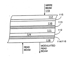
transmission mode in Fig. 5A, positions an analog planar-
aligned chiral smectic LC cell half-wave plate (50), e.g.,
a SmA* or DHF cell, between two quarter-wave plates ~51 and
52). ~he smectic LC cell (50) comprises transparent or
semi-transparent substrate walls, transparent electrodes
and optional alignment layers (not represented). The width
of the LC layer in the cell is chosen so that the cell is
a h~lf-wave plate for the wavelength(s) to be modulated.
A basic principle for optical modulation with this
device is that conversion of incident linearly polarized
light to circular states of polarization via the quarter-
wave plate allows the induction of an absolute phase
retardation through a smectic LC half-wave plate, without
a change in the state of polarization. Passage through ~he
second quarter-wave plate reconverts the circularly
polarized light to linearly polarized light~ The resulting
phase shift is ;a function of the orientation, e, of the
ha}f-wave plate with respect to the direction of
polarization of incident light and is, thus, a function of
j 20 the voltage (or e}ectric field) dependent tilt angle of the
1~ smeatic LC material. Voltage dependent rotation of the
optic axis of the~smectic LC produces an analog change in
phase which in~ transmission mode results in analog
modulation of intensity of incident coherent monochromatic
light or in anaIog modulation of the wavelength of incident
non-monochroma~ic light. The quarter-wave and half-wave
~ plates are preferably achromatic over the wavelength region
I of interest. As~ indicated in Figure 5, the optic axes of
quarter-wave plate(s~ of the phase modulator are parallel
or perpendicular to each other and are oriented at ~45O to
the direction of polarization of incident light.
1~ ~ The device~of Figure 5B is configured for reflection-
J~ mode operation by adding an approximately lO0% reflective
surface (53). ~Reflective surface (53) may replace one of
the transparent substrate walls of the CSLC cell (50).
This reflection ~mode device requires only one quarter-wave
plate (51) and the smectic LC cell (50) is designed to be
a quarter-wave plate for the wavelength of monochromatic or
1~ :
Y~
~ W093/l0477 PCT/~92/~g707
2123310
: 32
coh~rent light to be modulated. The reflection only device
operates as a pure phase modulator.
The Jones matrix describing the composite structure of
Figure 5A is given by (~.D. Sharp, Ph.~. Thesis, Univ. of
Colorado, 1992)
~(~) ella~A~ e o I (14~
where ~ /4), and ~A and ~u are the common phase
fackors due to the quarter-wave and half-wave plates,
re~pectively. This can be reognized as a single retarder
, 10 orien~ed at angle 0 (with respect to the z axis~ with
retardation 4~.
The phase nodulator of Figure 5 is a specific example
of a variable retardex implemented with a planar-aligned,
~ analog CSLC cell. In this example, the input light is
`~l 15 linearly polarized and oriented at oo. In the generalized
., case, a variable retarder comprises the same elements as
the modulator of Fisure 5. However, the polarization of
l the input light can be elliptical as well as linear and can
;7 ha~a any orientation. Equation 14 describes the co~posite
1 20 structure of the general ~ase.
Fig~re 6 illustrates an optical modulator of this
invention comprising the analog phas~ ~odulatcr of Figure
5 .within a resonance cavity operating in
transmis~ionlreflection mode. The numbering of elements in
Figure 6 is the same as in Figure 5. The resona~ce caYity
of the device of Figure 6 is formed by refl~ctive surfaces
61 and 62, which are parallel and opposed su~h that light
ent~ring the resonance cavity is reflected at least once.
f The resonanc~ cavity has length, L, and extends between the
reflective surfaces, at least one of which is transmissive
to allow light to enter the resonance ca~ity. The wa~e
~: plates are po~itioned parallel to and between the
reflective surface~. The optic axes of the two quarter-
wave plates 51 and 52 are oriented at an angle of ~45 with
respect to the direction of polarization of linearly
polarized incident light (i.e., at 45 to the plane of
vibration of incident light). The cavity may optionally
,~, , ,= .. , .. .~ . ..
1 WO93/1~77 212 3 31~ PCT/US92/09707
33
include one or more isotropic layers (e.g., 63) aligned
parallel to the wave plates ser~ing to alter the length of
the resonance cavity if so desired.
The operation of the etalon of Figure 6 in
transmi~sion/reflection mode is as follows: Linearly
polarized, monochromatic or coherent light of the design
wavelength is illuminated into the etalon along a
propagation axis through the reflective surfa~es and wave
plates. In transmission mode, modulated light is analyzed
or detected on the opposite side of the device from which
it ~nters the etalon. A variable voltage sr electric field
is applied to the electrodes of the LC cell to rotate the
optic axis of the cell in the plane of the substrate walls
~-, which form the aperture of the smectic LC cell. The
optical axis of the material can be rotated from ~~x to
+~ (a total of 2~x) by application of a maximal voltage -
V~ or ~V~, respectively, where ~x is the maximum voltage
~ dependent tilt angle intrinsic to smectic LC material.
bl Rotation of the optic axis of the smectic LC modulates the
intensity of monochromatic, coherent light. An exit
polarizer is not required to detect intensity modulation.
Analogously, the wavelength of non-monochromatic linearly
polarized light is modu1ated by the device of Figure 6 and
polarization analysis is~ not required to detect the
wavelength modulation.~
Assuming that the etalon mirrors have the same
reflecti~ity~(R) and that there is no mirror absorption,
the intensity ;transmission function for the device of
Figure 6, can be expressed as ~Sharp, Ph.D. Thesiæ, p. 180)
~] 30 ~ : T(A) - ll R)2+4Rsinz(~2~) (15)
~` where ~ is the~sum of all absolute phases accumulated in
the cavity in ~a single pass. Using reasonably high
reflecti~ity mirrors (e.g., R>85%), this function is
3S characterized ~y a series of narrow spectral peaks (with a
~;~ theoretical unity transmission) separated by broad bands
~:
,. .
WO93/10477 . PCT/US92/09707
2123~10 34
with strong rejection. Transmission maxima occur when the
sinusoidal term in the denominator of Equation 15 vanishes,
, or
~+2~-m~ , (16)
, ' .
5where m is the order of the cavity resonance. ~ecause each
of the absolute phase factors is completely arbitrary, the
~ total phase factor c~n be expressed in the following manner
.' without sacrificing the generality of transmission function
lO~_ 2AL , (17)
.~ ~here L represents the distance of a single optical pass
;l throu~h the device (or actual cavity length thereof].
Substituting the above expression into Equation l6, the
wavelengths of peak transmission can be calculated.
15In order to electronically tune or shift the spectral
p~k transmitted by the davice of Figure 5, the molecular
director of the smectic LC half-wave plate is rotated so
that:the angle ~ is varied to a ~x~ When the optic axis
of the FLC is aligned with the polarization of incident
20light, i.e., ~ - 0, maxima of order m, and (m l~ occur for
~ m12L and ~1 _ (m-l) , (18)
?1 respectively. Th difference in these expressions gives
the Free-Spectral-Range (FSR) (~ ), which is the
25wavelength separation between transmission maxima
~1- 1 1/~ . (19
By changing ~, the resonance of order m shifts from
Ao~ 2L ~O la~ 1 (2 //~m~ (20)
, . .
WO93/10477 PCT/U~2/09707
~` 21233~L0
The difference of the two expressions in the above
equations, ~ , represents the spectral shift due to
the electro optic tuning of the analog CSLC
~ aA2/~L (21)
" ~7~;
,,
Allowing ~ A, the rotation of smectic LC molecular
director required to tune the analog device of Figure 6
through a FSR is ~ = ~/2. Currently, analog SmA* materials
are commercially a~ailable which are capable of yielding
tilt angles (~) greater than ~/8, h~nce, total director
~0 rotations exceeding ~/4, thereby permitting analog tuning
over a range greater than one-half of a FSR with a single
SmA /liquid rystal cell.
The device of Figure 6 also functions as an analog
I intensity modulator of monochromatic or coherent light
1 15 with, for example, a planar-aligned surface stabilized SmA
LC. Assuming a monochromatic or coherent input, the device
~' optical thickness can be selected such ~hat the
IJ . tran~mission, with a large negative bias ~10: V/~m~ applied
to the modulator, is unity. A sli~ht change in voltage
pro~uces a small phase: shift in the c~vity adequate to
~` ~hift ~ the wav~length of the device resonance by a
t3l signi~i~ant perce~nta~e of its ~pectral w}dth. This, in
turn, GaUSeS a ~harp~change in the intensity transmitted by
the device. ~For a phase change of ~/2, the transmission at
, 25 he w~velength of incident light is midway between the mth
and (m+l ) ~h resonance corresponding to a minimum in
transmission. This approach provides analog optical
ii~ intensity modulation without resor~ to the large Y~ltages
~,i which are required:to:produce a very small change in the
index of refrac$ion of the electro-optic materials in prior
i:~
'i art Fabry-Perot electro-optic modulators.
.` ~
W093/10477 PCT/US92/09707
2123310 36
The achievable contrast ratio, TMAx/TMIN~ is given by
C ~ 4R 2sin2(~) , (22)
where the maximum contrast ratio occurs for ~x = ~/8. The
design of ~he resonance cavity depends upon the application
requirements. A particular design, for example, might
require a high contrast ratio, while another might require
linearity in the transmission versus voltage
characteristic. From the above expression, it can be seen
:l 10 that high contrast ratio is achieved a~ the expense of
il linearity. ~he contrast ratio, while varying with tilt
, angles, is much more sensitive to the reflectivity of the
.l mirrors. This is because the change in transmission occurs
'~ rapidly near resonance, but flattens out quickly~
Consider a modulator containing intracavity a single
SmA* FLC cell positioned between parallel polarizers, with
an SmA* cell being designed to be a half-wave plate at the
wavelength of incid~nt radiation. For a 20 to~al range of
rotation in the FLC molecular director, the contrast ratio
is c = 1.7. This contrast ratio is comparable to the output
of a typical Fabry-Perot de~ice containing a material with
the same range of tilt. ~ mirror reflectivity of R = 0.7,
0.8 and 0.9 results in a contrast ratio of c = 14, 34 and
150, respectively. Figure 7 shows the xelationship of
transmission versus mo~ecular rotation, ~, for- three
dif~erent mirror reflectiviti~s~ R = 0.7, R - 0.8 and
R - 0.9. Figure 7 demonstrates that the slope near
~l resonance increases; as: the contrast ratio increases,
-~ thereby reducing the resolution and requiring accuracy in
tuning of de~ice. In:other words, for a device condition
near resonance, a very small change in voltage appli~d to
the cell can produce a large change in the transmission.
Figure 7 shows the slope corresponding to R = O.7, or the
lowest contrast ratio, is:most linear. On the other hand,
.~, 35 the slope representing R - 0.9 is highly non-linear,
wherein a 5 change in ~ effects a substantial transmission
~.,
,
. . .
WO93/10477 212 3 31~ PCTtUS92/09707
37
change from unity to 8%, while a subsequent angular change
of 15 produces only a minimal transmission change from 8%
to 0.7%. Thus, a high contrast is exhibited with a highly
nonlinear transmission function.
The modulator o f Figure 6 can be operated in the
reflection-only mode to give pure phase modulation of
incident linearly polarized, coherent, monochromatic light
as is illustrated in the device configuration of Figure 8.
Operation in reflection only mode requires that one o~ the
reflective surfaces, i.e., 62 be approximately 100%
reflective. The resonance cavity thereof operates to fold
the optical path numerous times thereby effecting a long
effective interaction length. The increased interaction
length in turn produces a large phase change with only a
small rotation of the molecular director.
I Figure 8 shows an exemplary configuration of an analog
¦ tuning asymmetric Fabry-Perot~phase modulator operating in
reflection-only mode comprising a resonance cavity formed
by a front reflective surface (81) having Rl < 1, a
quarter-wave plate (83) for the design wavelength to be
modulated, an analog chiral smectic LC cell (80),
preferably planar-aligned, which is a quarter-wave plate
for that design~ wavelength and a back reflective surface
(82) having R~ The optic axis of the quarter-wave
platé l83) is~oriented at 45 with respect to the direction
of polarization of incident light. The electrodes (not
illustrated in ~Pigure 8) of the smectic LC quarter-wave
plate are connécted to a variable voltage source in order
~ to tune the phase modulator. The coherent, monochromatic
1 30 ~ linearly polarized light beam of design wavelength is
; illuminated, along the axis normal to the mirrors, through
the device.
The follow~ing mathematical description of the
¦ ~ reflection-only mode phase modulator is analogous to that
~35 provided above for the transmission mode device and is
i based on the assumptions that the amplitude of the light is
unaffected by the reflective surfaces, the back reflective
.
~ WO93/10477 PCT/US92/09707
~12331l) 38
sur~ace is an ideal, no-loss, reflector and incident
radiation is propagated along the axis normal to the
confining ~ubstra~e plates of the device.
The Jones matrix for the round-trip of light through
~, 5 the device of Figure 8, due only to the two wave plates, is
the same as for the transmission mode devi ce of Fig. 6 .
The total filed reflected by the device is
ii
,,
il r t2e~ 2~ (23)
~ 1 - r e~ 2~)J o
,~ .
where t and r are the complex f ield transmission and
reflection coefficients of the front mirror. Assuming no
mirror absorption, the reflected intensity is equal~to the
i, incident intensity, and the relationship between the
complex reflection and transmission coeffici~nts can be
determined. Since the device is assumed to have no energy
lS losses, the reflection coefficient for the phase modulator
can be written as
r - eix (~4)
where X is the induced phase shift. Assuming that the
phase is zero for ~ = 0, or ~/2 = m~, where m iS an integer
representing the order of the device, the phase expression
is
X - 2tan~ +~)tan~l . (25)
(1-~ O J
~ . :
The induced phase shift SX) is a direct consequence of the
rotation of the smectic LC molecular director~ This ph~se
25 ~ shift is enhanced by the gain term due to the reflectiYity
of the f~ont mirror.: ~
Figure 9 show6 a series of resultant phase shift X(~)
for different Rl values of the front mirror. A SmA*
: material which has a maximum tilt of 10 is assumed in this
~, 30 analysis. Clearly, for Rl = O, the gain factor is unity,
and the phase change is limited to a maximum of ~2~. This
condition represents the linear solid line shown in Figure
WO93/10477 21 2 3 3 10 PCT/US92/09707
39
9. For Rl = 0. 7, a dramatic change in modulation depth is
observed over the previous case as ~hown by the dotted line
of Figure 9. Under this condition, the phase shift through
the device can be ~uned continuously from -126 to 126~
As Rl increases, the maximum achievable X saturates toward
~ and the phase function becomes more nonlinear. For Rl
= 0.8, the phase shift can be tuned from -145 to 145.
For Rl = 0. 9, the phase shift can be tuned from ~163 to
163. Finally, for Rl = 0. 97, th2 phase shift can be tuned
from -175 to 175. Since the maximum phase change ever
required is 2~, the analog phase modulator of Figure 8,
permits a broad ~nalog tuning range over 97% of the maximum
range.
In other exemplary modulator embodiments, the
reflective surfaces whi~h form the optical cavity are
~l external to the CSLC cell and the optical cavity can
optionally include more than one of such cells. Two or
more of the same type:of CSLC cell can be combined or two
or more of diferent types of cells can ~e combined.
Particularl~ useful co~binations of CSLC cells within an
¦ optical cavity include~ cascaded planar-~ligned, surface-
1 stabilized Sm~; cells (where ~x < 45) to increase the
¦ total rotation o~ polarization of incident light preferably
to 90 and combinations:of DHF cells with similarly aligned
SmA~ or SmC cells in which the SmA or SmC cell functions
to compensate for the induced polarizati~n of the DHF.
Also useful are: combinations of two (or more) DHF cells
i whose optical axes rotate in the same direction to
compensate for ~he rotation of polarized light or that
rotate in opposite directions to compensate for the change
;~ in birefringence~ These cavities can also optionally be
provid~d with an isotropic spacer between the reflective
surfaces external to the chiral smectic liquid crystal
cell( ~ to allow the cavity length to be changed. These
modulators can optionally be provided with intracavity
len es which function to focus light reflected within the
cavity to minimize 105s. Analog phase and wavelength
.~ ,
W093/10477 PCT/US92/~9~07
, .
2123310 40
modulators can be provided by incorporation of quarter-wave
plates as described aboveO
'IV. Exem~lary Applications of_the OPtical Modulators_of
~b~
i 5The optical modulators of the present invention can be
electronically or optically addressed. Exemplary
embodiments of optically addressed modulators include
configurations having photosensors, for example, using
crystalline silicon or GaAs, or a thin film of an amorphous
~ 10silicon, CdS, CdSe, GaAs, or functional equivalent
¦photodiode~ or photoconductors.
A single-pass transmission modulator is illustrated in
Figure 10. Surface-stabilized CSLC material is employe~ in
half-wave retarder 100, which is flanked by quarter-wave
15plates 106 and 107 to make a variable retarder. The device
further includes substrate walls (101 and 102), transparent
electrodes (103 and 104), and a photosensor (105).
A specific embodiment of an optically addressed etalon
modulator of the pr~sent invention îs a modification of
1 20spatial light modulators as described, for example, by ~.
Moddel et al. (1989) Appl. Phys. Le ff . 55(6):537 and I.
Abdulhalim et al~(l989) Appl. Phys. Lett. 55 ~16):1603.
.,
.One ~pecific reflection-only-mode phase modulator
configuration: is; provided in Figure 11. The exemplary
2~device: of. Fiqure~ll consists of transparent or semi-
,~transparent substrate walls (117 and 118), e.g., made from
glass, and contains a~pho~osen or layer (110) which can be
a photodiode, for example, a hydrogenated amorphous silicon
photodiode or a photoconductor. One of the substrate walls
30is provided with a transparent electrode (115), e.g., a
metal oxide film. ~he~:optical or asymmetric FP cavity is
.~formed by reflective surfaces (113 and 114). The other
-ubstrate wall is provided with a transparent electrode 116
or the reflective surface I14 may serve as the second
3Sele~trode. For a reflection-only mode modulator, the
` reflectivity of 113 is ideally 1, and the reflectivity of
`'
.
' WOg3/1~477 PCT/US9~/09707
2123310
41
114 is < 1. The reflectivity of 113 should be sufficiently
higher than that.of 114 so that a significant portion of
~;' the incident light exits the cavity through 114 and 118.
, The deYice is provided with a planar-aligned layer of a
, 5 chiral smectic liquid crystal material (111), for example,
,~ a surface-stabilized~ planar-aligned SmA or SmC material,
'~l the optic axis of which is rotatable by application of an
electric field across the layer. The device of Figure 11
'', may also include alignment layers adjacent to the chiral
ii, 10 smectic liquid crystal layer to assist alignment of the
i material. A square-wave clock voltage with an optional dc
.1 offset i5 ~pplied between the electrodes 116 and 115 and an
. electric field is generated across the CSLC layer when an
`3 optical signal, i.e., the write beam (119), interacts with
5;~ 15 the photosensor layer ~110).
'' ~ binary or ternary phase modulator results when a
,l discrete planar-aligned, surface-stabilized chiral smectic
' liquid crystal layer is employed in layer 1~1. The
orientation of the optic axis of the layer is switched by
~;i 20 the optically activated, electri~ field placed across the
~ CSL~ during the negative cycle of the square-wave clock
il voltage. The:de~ice optic axis is switched back during the
~l positiv~ cycle of the square-wave clock voltage. Switching
'~i the orientation of the optic axis of the CSLC layer
~l 25 modulates linea~ly polarized light entering (the read beam)
the modulator through substrate 118. ~odulated light exits
t~e device through substrate 118. An exit polarizer or
polarization analyzer is not required to detect light
! modulation.
An analog phase modulator results when an analog
. planar-aligned/:surface-stabilized chiral smectic liquid
`~, crystal materiaI is employed in layer 111 and when a
~` q~arter-wave plate (112~ is included in the modulator. In
.,~ reflsction-only-mode, the CSLC layer is preferably a
., 35 quarter-wave plate for the wavelengths of light to be
, modulated.
`: ~
'~' `
~,';1j
.~
WOg3/10477 PCT/US92/09707
,,
2 12 33 10 42
Optical addressed intensity and wavelength modulators
operated in transmission/reflection mode can be implemented
.~ by configurations similar to that of Figure 11, uæing the
descriptions of the preæent invention and well-known
techniques of optical addressing.
In some embodi~ents, the reflective function of the
, reflective surface tll3) can be performed by the interface
between the photosensor layer (110) and the liquid crystal
layer (1113. If the difference in refractive indices
between the materials employed for 110 and 111 is large
enough, that interface will function to reflect light and,
~i thus, function to form th2 etalon cavity.
An analog, planar-aligned optically addxessed
intensity and wavelength modulator operated in
transmisæion/reflection-mode, a modification of the device
of Figure 11, r~quires two quarter-wave plates in the
resonance cavity on either side of the analog CSLC half-
wave layer. In a wavelength modulator, the quarter-wave
plates are preferably~achromatic.
The optical modulators of the present invention can be
.l fabricated as multiple pixel devicas. Several exemplary
`I embodiments of multi-pixel modulators are provided (in
Figures 12-14).:~
~. ~LSI tVery Large Scal~ Integration) integrated circuit
i 25 backplane re~r~sents a means for electrically addressing a
~, ~
multi-p~el chixal smectic liquid crystal FP or folded
: optical path device~. Such multiple~ pixel devices can be
operated in transmission/reflection- or reflection-only
mode. m e desired chiral smectic liquid crystal material
;:. . . . .
is positioned and appropriately a~igned between a substrate
. ; overlayer and~a ~VLSI backplane which comprises pixelated
~, ref~ective surfaces. The substrate overlayer is provided
- with~ a reflective surface, such that multiple pixel
resonance cavi~ies are created between the opposing
,:1
`' 35 reflective surfaces of the substrate overlayer and the VLSI
backplane. One or two birefringent elements, in particular
quarter-wave plates can optionally be included in such a
i :
W093/10477 PCT/US92/~707
- 212~31~
43
multi-pixel device between the CSLC material and ~ither of
the reflective sur~aces. The individual resonance cavities
of a multi-pixel device produced in this manner function as
the individual CSLC modulators of this in~ention as
described herein-above. The type of modula~ion is
dependent on the mode of operation of the ca~ity, the type
of alignment employed, the type of CSLC material employed
and the tilt angle and birefringence of that material.
~ A multi-pixel, binary phase, intensity or wavelength
;~ 10 modulator, as in Figure 12, results from the inclusion of
a planar-aligned layer of a SmC~ material (120) having a 45
tilt angle between a VSLI backplane (125) comprising
pixelated reflective surfaces (121) and a substrate
overlayer (126) having a reflective surface that is less
than 100% reflective (122). When the pixelated reflective
surfaces tl21) are also Iess than 100% refl~ctive and the
VLSI device is operated in the transmission/reflection
mode, binary intensity or wavelength modulation results.
, When the back reflective surfaces (121), i.e., those
l 20 of the VSLI backplane, are of significantly higher
`, reflectivity than the front reflective surface (122), the
device operates in reflection-only-mode, and a binary phase
modulator results. The intracavity CSLC layer (120~ is a
Sm~ 45 tilt angle material (planar-aligned and surface-
: . ~
~ 25 stabilized). In the device of Figure 12, the reflective
3 ~ surfaces, e.g., deposited~ metal mirrors, also serve as
~' electrodes. Polarized~ coherent light incident on the
modulator is phase~ modulated by passage through the SmC
layer. Polarized monochromatic incident light and
polarized non-monochromatic incident light are intensity
and wavelength-modulated, respectively, by the device of
Figure 12. ~ ~
Another exemplary pixel of a VSLI configures
~ ~ reflection/transmission mode modulator is given
`~35 schematically in~ Figure~13. This modulator can function
, either to modulate the intensity of monochromatic or
i ~ coherent light, or to modulate wavelengt~ of non-
.
~'
",:
. ~
,~ W093/10477 PCT/US92/Og707
2 L2~31~ ~4
monochromatic light. A pixelated VSLI backplane (135)
provides a substrate with one reflective surface ~131). A
substrate overlayer (136) is provided with a second
reflective surface (132). Within the reso~ance cavity
formed by the reflective surfaces, . there are two
birefringe~t elements, specifically two quarter-wave plates
(133 and 134). A layer of a planar-aligned, surface-
stabilized SmA~ liquid is provided (130). The reflecti~e
~¦ surfaces 131 and 132 also serve as electrodes in this
~j 10 configuration. The thickness of the layer is chosen such
that the SmA liquid crystal cell (130 between 131 and 132)
is a half-wave plate for the light to be modulated. The
quarter-waveplates used in the wavelength modul~tor are
.l preferably achromatic.
~i 15 Yet another exemplary pixelated modulator is provided
~:~ in Figure 14. In this example, a homeotropically-aligned
CSLC layer (140) is employed within a resonance cavity
formed by a back reflective surface (141) and a front
reflective sur~ace (142) on substrate walls ~14S and 146).
Lateral electrodes are provided (143 and 144) with optional
¦ insulators between the electrodes and reflective ~urfaces.
.~l These electrodes can be patterned, for example, to create
~ a multi-pixel ~array. The figure illustrates a
. transmission/refl~ection-mode device in which the
;l 25 reflectivities~ of; 141 and 142 are both less than 1.
Intensit~ and:~wavelength modulation of incident light can
; be performed by~:this :device configuration. Any CSLC
:~ material can ~e~ employed in the homeotropically-aligned
. cell of Fi~ure 14. Discrete state CSLC materials give
discrete modulation. Analog CSLC materials give analog
modulation. : ~
Examples of optically addressable, multi pixel, binary
and analog modulators are analogous to the VLSI
; configurations de~cribed above, except that the V~SI
35` integrated circui~ :is replaced with means for optically
addressing the multi-pixel array, including a photosensor.
One type of multi-pixel FLC spatial light modulator is
~`
r~"
W093/tO477 2 1 2 3 3 1 0 PCT/US92/~707
described in G. Moddel et al. US Patent 4,941,735. Optical
addressing of CSLC cells has been described in Takahashi et
al. (1987) Appl. Phys. Letts 51:19; Moddel et al. (1987~
"The Proceedings of SPIE - The International Society for
Optical Engineering 759:207-213 and Ashley et al. (1987)
Applied Optics 26:241-246. Teachings of these references
regarding optical addressing can be readily applied by
those of ordinary skill in the art to the devices of the
present invention~
The multi-pixel modulation herein can be
electronically addressed or optically addressed as in known
I in the art. The individual pixels of these multi-pixel
;, devices can be individually addressable, simultaneously
add~essable or certain combinations of pixels may be
lS simultaneously addressable in desired patterns. Multi-
pixel chiral smectic liquid crystal FP optical cavities
modulators can be employed for a variety of display
applications, including diffractive optical elements and
holographic displays and~can in addition be employed by
~20 appropriate choice of addressing schemes to create
,1 ~ patterned modulators,~for; example to create a pattern of
~ lines to generate a~diffraction grating for beamsteering
3 applications. ;~ The operation of ~such beamsteering
diffractive grating~is understood in the art.
Another ~ exemplary application of a
transmission/re1ection mode CS1C etalon modulator of the
,
` present invention~is the so-called "tunable tap" of Figure
15. This ~device provides a ~eans for "tapping" or
~, selecting a desired wavelength of incident non-
' 30 monochromatic light while minimizing overall loss of total
~l light intensity.~ ~The device of Figure 15 comprises two
polarizing beam splitters (153 and 154), a Faraday retarder
' (155) and two reflective surfaces (157 and 158) forming a
`~ resonance cavity on either side of a planar-aligned CSLC
analog wavelength modulator (150-152) and two total
internal reflectance mirrors (159 and 160) with elements
positioned relative to each other as indicated in Figure
. .
~ WOg3/10477 PCT/USg~/09707
.....
2123310 46
15. The figure also indicates an input (A) and two outputs
(B and C) for light. The planar-aligned CS~C analog
- wavelength modulator is exemplified as a planar-aligned
CSLC half-wave plate ~150) with two quarter-wave plates
(151 and 152). '~he CSLC material employed is any planar-
aligned analog material displaying a voltage-dependent
;~ rotation of its optic axis. Preferably, the CSLC material
is a planar~aligned, surface-stahilized SmA~ ~aterial. ~he
~uarter-wave plates of the analog modulator are oriented at
0 or 90 with respect to light entering the resonance
cavity.
: Unpolarized light enters the device at input A and
PBSl tl53) splits the incident light of the beams i~to two
orthogonally polarized beams. A Faraday retarder (155)
. rotates the polarization of both beams by 45O. The
operation of ~araday retarders is well known and understood
in the art. Light enters the resonance cavity containing
the modulator. The output PBS2 (154) is oriented at 45 to
the input PBSl (153). The rotated light exiting the
~0 resonance cavity is then split by PBS2 so that a selected
wavelength is transmitted to output C while the remaining
light is reflected~from I58 back through the resonance
cavity. (The~ resonance cavity is formed between the
. reflective surfaces (157) and (158) with reflectivities R1
;! 25 and R~ An electric ~ield is applied to the modulator
~across -'the: CSLC layer of the modulator) via cell
~i electrodes (not shown) to select a wavelength for
transmission to output port C. The wavelength that
satisfies the condition
" 2 Jc~nL ( ~ 6 j
~; j h
!'l where ~ is the selected ~, ~n is he birefringence of the
cavity, L is the cavity length and m is an integer, is
~ transmitted to the output C. All oth~r wavelengths of
"5~ ~ ~ incident light are reflected back through the cavity and
are transmitted through output port B.
~: :
~` .
.
WO93/1~77 2 12 3 31 0 PCT/US92/09707
47
While certain illustrative device configurations and
: application of the light modulators of the present
invention have been described in detail in the
specification, it should be understood that there is no
, 5 intention to limit the invention to the specific forms and
'. embodiments disclosed. On the contrary, the invention is
: intended to cover all modifications, alternatives,
equivalents and uses fully within the spirit and scope of
the invention as expressed in the appended claims.
,
I ~ .
'l :
~ ' ;
J -
.
l ,
~ ~ :
~ :
j
'~ :
,~1
~ !
.,
WO93/10477 PCT/US92/09707
,
2123310 48
TABLE l: EXEMPL~RY oPTICAL CAVITY CSLC MODULATORS
Type of Modulation2
SType of CS~C Mode of1
Material Operation Phase IntensitY Wavelenqth
Planar Ali~nment
SmC T/R +(B) ~3
tilt ~ = 45
R +(B)4
SmC T/R +(B) ~(B)
tilt ~ = 45
R +tB)
SmA T/R ~(A) ~5
lS R +(B)4
DHF TjR +6 ~6
, R +(A)
i :
Antiferro- T/R : +(T) ~7
electric : :
: 20 R +(B)4
~' SmA ~T/R : +(~) ~(A)
quarter
wave(s) '~ R : : ~+(A)
;~ SmC T/:R ~ ~(B) +~B)
~ quarter-
. ~ wave(s) - R ~ +(B)
DHF T/R ~(A) +(A)
quarter- : :
1 ~ wave(s) :R +(A)
!~:
30SmA /SmA8 T/R +(A) ~8
~: oppOsit~4
: R +(B)8
(
.
' WO93/10477 1 2 3 ~ 1 0 P~T/US92/~9707
i 2
~g
TABLE l (continued)
Type of Modulation2
Type of CSLC Mode o~'
~; 5 _MaterialOperation Phase Intensitv Wave1enq~h
DHF/SmA10 T/R +(A) +(A)
.. Same
; R ~(A)
. .
' DHF/SmA12 T/R +(A) ~12
5,, l0 Opposite
i R ~(B)1
.,
DHF/DHF13 T/R +(A) ~13
' opposite
: ~ R +(B)3
. ~
DHF/DHF14 ~/R ~(A) ~(A)
5~ Same
~, R ~(A)
~'1
Sl~ Homeotro~ic ~liqnment
,
. SmC ~/R +(B) ~B~
`' 20 tilt ~ $ 45
or = 45 ~ +(B)
, SmA /homeo T/R +(A~ +(A)
~,~
R +(A)
.'- ,
~ D~IF T/~ ~ (A) + (A)
,; ~
~ 25 R +~A)
,j, , ; . , ,
Antî~erro- T/R +(T) +(T)
~. electric
c R ~(T)
~'^'j
~!
'
,, ,
WO93/10477 - PCT/US92/0~707
~123310 50
TABLE 1 (continued~
Footnotes to Table 1.
"TIR" represents transmission/reflection~mode and "R"
represents reflection-only~mode.
2 Many of the modulators of Table 1 effect a phase
change in tran~mis~ion/reflection-mode which is
detectible as inkensity or wavelength modulation. A
"~i' indicates detectible modulation, "B" represents
binary, "A" represents analog and 'tT" represents
ternary. Incident coherent light is phase modulated,
incident monochromatic and/or coherent light is
intensity modulated and incident non-monochromatic
: light is wavelength modulated.
I 3 This modulator selects between an output transmitting
1 15 one wavelength and an output transmitting two
wavelengths.
~', 4 This modulator selects between two phases of input
light, but output of a selected phase will not
l necessarily have same direction of polarization.
I 20 5 For non-monochroma ic incident light, this device
., provides analog intensity modulation of two selected
wa~elengths.
" 6 In planar-aligned ~HF devices there is a change in
,
birefringence of the CSLC layer and a rotation of
. 25 polarization of incident light on application of an
electric field to the device.
7 This modulator selects between one output transmitting
one wavelength and two other outputs transmitting two
wavelengths at different intensities. Similar to SmC~
~l 30 planar-aligned tilt ~ ~ ~5O.
`1~ 8 optic axes of SmA cells within a series in resonance
cavity are rotated in opposite directions to leverage
.l rotation of polarization of incident light. Intensity
modulation is analog. Wavelength modulation is
similar to (footno~e 5, above) except that when both
~`
W~93/10477 ~ PCT/US92/09707
. 2l233la
51
TABLE 1 (continued)
SmA~ cells have ~ = 22.5, wavelength ~odulation is
binary. Phase modulation is similar to that in
footnote 4, above, except that when ~x f both cells
is 22.5 phase modulated light exits with the s~me
direction of polarization.
9 "Opposite" indicat~s that the optic axes of cells
rotate in opposite directions.
10 DHF a~d SmA cells in series with optic axes rotating
in the same direction and to the same extent. This
cell combination effects a change in birefringence.
"Same" indicates that the optic axes of cells rotate
. in same direction.
', ~2 DHF and SmA cells in series with optic axes rotating
~ 15 in opposite directions to the same extent exhibit no
¦ cha~ge in birefringence. This cell combination
behaves like two planar-aligned SmA~ cells in series.
13 Two DHF ~cells:in series whose optic axe~ rotate in
opposite directicns and to the same extent. The
device:exhibits no birefringence changa. Similar to
combinations described in footnote6 8 and 12.
14 Two DHF~cells in series whose optic axes rotate in the
i! same direction and to th~ same extent. The device
.1 ; ;exhibits no rotation of polarization of incident light
;' 25 but-:exhibits ~an increase in the change in
birefringence. ~The modulator functio~ to that of
footnote 10.
'i !
~1:
~`
! ;
~! .