Note: Descriptions are shown in the official language in which they were submitted.
WO 93~10~;73 - PCI`/US92/10044
2123877
DI~3 MO~ING WIT~I ~NIAXIAL ~ :
CONDlDCq~IVE~ E8IVE . :~
TEClEINICAL FI~I.D -
The subject invention relates to
electronic devices and electrically conductive
adhesive there~ore. More particularly, the
invention relates to the connection of an ,
electronic device to a substrate using a uniaxial
conductive adhesive. '~
: :
BACXGROlJND ART :
::
In many electrical applications, it is
desirable to connect an electrical component with ~ ~'
or without conductive terminals leads extending ~;
therefromr to a substrate including a plurality~
' of laterally spaced çonductive paths. A current
is passed between the aligned conductor contact'
of the electrical component to the substrate ~ ''
path. It is undesîrable for current to pass
between the electrical contacts causing shorting
of the circuit. , ,
?s Conventional methods have connected
electrical components which include conductive
terminals leads extending therefrom~by soldering
techniques.~It is~also known~to use a uniaxial
oonductive,~adhesive resin for mounting~electrical
components having terminals extending therefrom,
as disclosed in~United States Patent Number
4,667,401 ~ssued May 26, 1987 in the,name of
Clements et al., common invent~or to the subject
application.~ The patent discloses~a uniaxial
conductive adhesive wherein pressure between two
members causes conductivity therebetween by
concentration of conductive metal particles
:
- ,
WO93/10573 PCT/US92/100~
21~3~77 2
within the resin, while the areas surrounding the
depressed members remain non-conductive.
United States Patent Number 4,113,981 ~ ;
to Fujita et alO, issued September 12, 1978 '
discloses an electrically conductive adhesive for
connecting raised conductors or terminals of
electronic devices. Pairs of connecting
terminals are attached to plates such that the
connecting terminals project from the surface of
the plates. Upon pressure of the plates to one
another, the terminal compressed the resin to
obtain conductivity between metal particles
within a resin. Portions between the plates
absent the terminals are not conductive due to ~
15 the left compression thereof as being recessed ~ -
from the connecting terminals.
United States Patent Number 4,640,981
issued February 3, 1987 in the name of Dery et
al. discloses electrical interconnection means
which utilizes two members having printed thereon
ink conductors. The members were placed facing
one another with an adhesive therebetween. In
order to obtain conductivity between the two
members, pressure is applied to an area of one of
25 the members to bring the conductive inks into ~ ;
contact with each other forcing the flow of
adhesive therefro~.
t is known in the art to deposit
~ layers to the conductive portions on the
eléctrical contacts of the electrical component
utilizing several plating steps, iOe. sputtering
which is generally very expensive and time
consuming. United States Patent No. 4,811,081 ;~
issued March 7, 1989 in the name of Lyden
discloses use of an anisotropically electrically
conductive adhesive which is used between a
WO93/10S73 212 3 8 7 7 PCT/US92/100~
projecting contact pad and conductive path on a
substrate.
However, this prior art is
inapplicable to electrical components which do
not have terminal leads or "bumps" extending
therefrom. In general, these type of components
include the passivating layer which is
discontinuous exposing recessed areas of
electrical contact pads. The passivating layer
may have a thickness of 0.3-0.9 microns and is
very fragile. The layer can not take the
pressure of the prior art and isotropic
adhesives. The above methods do not apply to
this type of an electrical component due to the
electrical contacts being recessed rather than
extending therefrom allowing pressure directly
thereon.
United States Patent No. 4,423,~35
issued December 27, 1983 in the name of Test, II
discloses use of an anisotropically electrically
conductive adhesive solvent which is placed
between contact pads and conductive paths of a
substrate. As the solvent evaporates, the resin
will contact predominantly along the Z axis
remaining non-conductive along the X- and Y-axes.
The resin is heated to activate the adhesive.
: ' ~ 8~NNARY OF TKB INV~NTION
The invention is a method of forming an
~ electronic device. The method includes the step
,~ of forming an electronic device comprising an
electronic circuit member having a discontinuous
insulation layer establishing recessed contact
pads, a substrate with a mounting surface having
conductive paths thereon and establishing raised
conductive surfaces vertically aligned with the
WO93/10573 ` ` ` PCT/US92/100~ ~
2~23877 4 :~
contact pads, the raised conductive surfaces have
a height greater than the height of the
conductive path vertically aligned with the :~
insulation layer, an adhesive between the circuit
member and the substrate having a resin and
spaced conductive metal particles suspended
therein with concentrated conductive particl~s
between the raised conductive surfaces and
contact pads allowing conductivity through the ~ :
10 resin making the resin uniaxially conductive ~ :
vertically therebetween while maintaining the
adhesive between laterally spaced contact pads
and co~ductive paths in the unconcentrated and
nonclonducting states.
Also included is a method including the
steps of providing a substrate having laterally
spaced conductive paths thereon, applying an
adhesive on the substrate having a resin and :`
spaced conductive metal particles suspended
20 therein being in an unconcentrated and non- ~ :
conductive state, placing an electronic circuit
member having a discontinuous insulation layer
establishing recessed contact pads over the
adhesive with the contact pads vertically aligned
with selective conductive paths, and applying
pressure to the circuit member against the :
substrate to concentrate conductive particles . between the conductive paths and contact pads
allowing conductivity through the resin making
the resin uniaxially conductive vertically
therebetween while maintaining the adhesive
: between laterally spaced contact pads and ~
laterally spaced conductive paths in the :
unconcentrated and nonconducting states.
The invention also includes an .
electronic device which comprises a circuit ~:
member mounted on the substrate. The circuit ~:
W093/10573 2 ~ 2 3 ~ 7 f PCT/USg2/10~
member includes a discontinued insulation layer ~ ~ ~
which provides electrical contact pads recessed ~ -
within the discontinuities. A substrate includes
a mounting surface having a plurality of
S laterally spaced conductive paths thereon with a^-
portion of the conductive paths establishing
raised conductive surfaces vertically aligned
with the recess. The conductive surfaces have a
protruding height aligned with the recesses
greater than the protruding height of the
conductive paths vertically aligned with the
insulation layer. An adhesive layer coating is
appl:ied to the raised conductive surfaces of the
conductive paths for adhering the circuit member
to the substrate. The adhesive includes
concentrated conductive metal particles between
the vertically aligned contact pads and raised
conductive surfaces and is uniaxially conductive
vertically therebetween, and unconcentrated and
non-conductive between laterally spaced
conductive pads and conductive surfaces wherein
the resin is a dielectric preventing conductivity
between the metal particles therein and being
non-conductive laterally therebetween.
-
FIGURB8 IN T~E DRA~INGS
~ Advantages of the present invention
will be readily appreciated as the same becomes
~30 better understood by reference to the following
detailed description when considered in
connection with the accompanying drawings
whereln:
Figure 1 is a plan view of a circuit
member mounted on a substrate;
::::
.::.
W093/10573-`-` ' PCT~US92/10~
~ .
2123877 6 `' } ~ ~
Figure 2 is a cross-sectional view
taken along lines 2-2 of Figure 1 of a first
embodiment of the subject invention;
Figure 3 is a cross-sectional view
5 taken along lines 2-2 of Figure 1 of a second - -~
embodiment of the subject invention;
Figure 4 is a cross-sectional view ~'~
taken along lines 2-2 of Figure 1 of a third ~'
embodiment of the subject invention; and ;~
Figure 5 is a cross-sectional view
taken along lines 2-2 of Figure 1 of a fourth
embodiment of the subject invention. ' ~
:,. :
:
DETAIIIED D~8CRIPTION OF THE .: :.
PREFERRED ENBODINENT
~: '
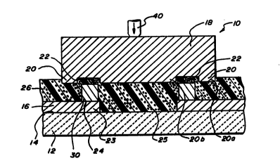
An electrical device constructed in ,'
accordance with the subject invention is ~ ~
20 generally shown at 10 in Figure 1. The device ~ '
includes a substrate generally indicated at 12.
The substrate 12 is a supporting material on or
in which parts of the circuit are attached or ''`~'
made. The substrate 12 may be passive or active.
The substrate 12 includes a mounting
surface 14 having a plurality of lateràlly spaced ,,,;
conductive paths 16 the~eon. This type of
substrate 12 is generally referred to as a
printed circuit board in which~normally~found
-interconnecting wires are replaced by,conductive,
strips~16~printed, etched or otherwise mounted
onto the insulated substrate 12. In other
words, the substrate is non-conductive, providing
insulation between the conductive paths 16. The ~;~
substrate 12 may also be referred to as a printed
circuit board or insulating board onto which the
conductive path 16 or circuits are printed. ~ ~
`~ ~ ',''..
WO93~10~73 212 3 8 7 7 pcr/us92/1oo~
Other substrate materials may be used, such as
printing onto polyester film or other polymer
films. The conductive material or ink utilized
as the conductive path 16, may be screen printed
using conductive ink as commonly known in the art
and may include other methods of applying
conductors as commonly known in the art. ~he
conductive path 16 has a height or thickness on
the order of 15-50 microns. The ink 16 is
generally a conductive polymer thick film of the
type Minico.
A circuit member is generally indicated
at 18. The circuit number 18 may be in the form
of any one of various types of electrical
components, such as capacitors, resistors,
integrated circuit, etc., or maybe in the form of
other semi-conductors. Alternatively, circuit
member 18 may be a second substrate mounted on a
first substrate 12.
The circuit member 18 includes a
discontinued protective, insulation or
passivation layer 20 thereon providing electrical
conductive surfaces or pads 22 recessed within
the discontinuities. The contact pads 22 provide
the means for external electrical connection with
the circuit member 18, as commonly known in the
art. The contact pads 22 are aligned vertically
over selected ones-of the conductive paths 16 in
the "flip-chip" technique but used with a die
without bumps thereon, herein after referred to
by applicant under his trademark of "flip-die".
Functionally, it is desirable to have uniaxial
..
electrical conductivity between the conductive
paths 16 and the contact pads 22, without
electrical conductivity between laterally spaced
conductive paths 16 or contact pads 22. The
circuit member 18 with the passivation layer 20 ;
WO93/10573 ~r: ,~; !;; PCT/US92/100~
~23877 8
is commonly known in the art and provides such
contact pads 22 recessed therein prior to the
common application of applying extending
conductive terminals therefrom or "bumps".
Protruding means 24 is operatively ^
provided between the contact pads 22 and a
terminal or end portion 23 of the conductive
paths 16 to decrease the distance or separation
between the contact pads 22 and conductive paths
16, as will be subsequently discussed. In other
words, the height protrusion of the terminal
portion or end 23 of the conductive paths 16
vertically aligned with the recessed contact pads
22 is greater than the height protrusion of the
conductive paths 16 vertically aligned with or
unde!r the passivation layer 20 providing a
projection toward the recess 22, the heights
taken with respect to the general plane of the ;~
substrate 12. The subject invention avoids the
requirement of producing "bumps" or connecting
terminal leads on the circuit member 18 of the
prior art. ~he protruding means 24 may be any of
several embodiments, as subsequently discussed.
A uniaxially conductive adhesive
coating 26 is disposed over the mounting surface
14 for adhering the circuit me~ber 18 to the
substrate 12. The adhesive 26 includes a resin
having approximately 40 or greater by weight
conductive metal between the vertically aligned
contact pads 22 and protruding means 24 of the -
terminal portion 23 of the conductive paths 16
and the resin is conductive vertically or
uniaxially therebetween. The adhesive 26
35 includes about 20-25% by weight conductive metal -~
between the laterally spaced contact pads 22 or
conductive paths 16 and the resin is theref~re
~WO93/l0573 212 3 8 7 7 pcT/us92/1on~
non-conductive laterally therebetween. The lower
percentage of metal filler in the adhesive 22 is
not sufficient to support electrical current flow
through the resin. The adhesive coating is of
S the type set forth in United States Patent -^
4,667,401 issued May 26, 1987 in the name of
Clements et al., and incorporated by re~erence
herein and as subsequently discussed.
The resin is a dielectric preventing
lo conductivity between spaced metal particles
therein. As shown in the Figures 2-4, the
percent by weight content of the metal particles
in 1:he resin is concentrated between the contact
pads 22 and protruding means 24 of conductive
paths 16 thereby decreasing the spacing between
the metal particles. The decreased spacing
allows conductivity through the resin providing
conductivity between the aligned and protruding
means 24 of the conductive paths 16. The metal
part,icles suspended in the resin between
laterally spaced contact pads 22 and protruding
means 24 of the conductive paths 16 are not
concentrated sufficiently to cause conduction. ;~
The resin prevents conductivity between spaced
metal particles. The effect achieved is uniaxial
conductivity between aligned conductive members
16,~22, 24 and insulation or nonconductivity
therebetween.;
In order to obtain the decreasing of
space between the metal particles, the contact
pads;22 and protruding means 24 must provide a
lesser distance than the~distance between the
passivating layer 20 and the substrate 12. This
occurs by increasing the height of the end 23 of
the conductive path 16 aligned under the recessed
contact pads 22. The three embodiments of the
protruding means 24 will be hereinafter
WO93/10573 ^` `;` PCT/US92/10~ ~
r~
2123877 lo ` :
discussed. Primed reference numerals indicate
similar components in each em~odiment having the
same base member.
In the first embodiment of the
protruding means 24 illustrated in Figure 2, a -
conductive pellet 30 is placed on the conductive
path 16 at the end 23 thereof to provide the
necessary protrusion toward the recessed contact
pad 22 for diminishing the distance to the
conductive contact pad 22. The conductive pellet
30 provides a protrusion of the conductive path
16 such that concentration of the metal particles
in the resin will occur between the pellet ~0 and
contact pad 22 achieving uniaxial conductivity
therebetween, while the portion 25 between the
sub~trate 12 and the passivating layer 20 and the
conductive paths 16 of the circuit member 18
remains nonconductive. The conductive pallet 30
has a thickness about half the thickness of the
20 conductive path 16, i.e., 7-25 microns, in order
to provide a protrusion height of 22-55 microns.
A first method of applying the pellet 30 is to
provide a second screening of the conductive ink
isolated to the end 23 of the conductive path 16
which wilI be aligned with the recessed contact
pad 22. The pellet 30 may also be added to the
conductive path 16 by any of the foll~wing
techniques: applying an condu~tive ink drop, ~ ~
applying a conductive adhesive by stenciling or ;
screening, plating conductive metals, or any
other method of forming a conductive pallet
thereon. Each of the methods are c~mmonly known
in the art to form conductive material on
substrates.
The second embodiment of the protruding
means 24', as illustrated in Figure 3, may be
formed by providing a recess or ridge 32' within
WO93/10573 212 3 8 7 7 PCTlUS92/100~
11
the substrate 12'. ~he ridge 32' formed within
the substrate 12' may be molded in the case o~ a
rigid plastic substrate 12, e.g., printed circuit
board, or embossed or debossed in the case of a
flexible substrate, such as a polyester film. -
Conductive ink which is applied thereover forming
the conductive path 16l will follow the contour
of the substrate 12' creating the protrusion 24'.
The conductive ink path 16 may be applied prior
to embossing to provide similar results. The
protrusion 24' will be aligned within the recess
to allow concentration of the metal particles in
the resin.
The third embodiment of the protrusion
means 24'', as illustrated in Figure 4, includes
the ink applied as the conductive path 161', in
the manner as commonly known in the art. With
the adhesive 26 " placed thereover, the circuit
member 18 " is pressed thereagainst wherein the
passivating layer 20 " is pressed and indented
into the conductive path 16 " forming a
protrusion 24 " which is aligned with the
recessed contact pad 22 ". The formed protrusion
24'' decreases the distance to the contact pads
22 " for concentration of the adhesive 26 with
the distance between the passivating layer 20 and
substrate 12 remalning greater therefore allowing
no concentration~of the`metal particles in the
~resin. A pressure of approximately 2 psi is ~;
required to deform the PTF 16'', enough pressure
to force the PTF into the recessed. The pressure
must~remain until the adhesive 26 " and PTF 16''
,. . . ~
is cured. Alternatively, the substrate 12 " and
circuit member 18'' combination may be laminated
between two plastic sheets 34 or paper which
retains the pressure on the substrate 12 and
circuit member 18'' to maintain the depressions ~
,' .....
- '
W093/10~73 PCT/US92/100
21238~7 ` 12
in the conductive paths 16 and provide the
projections 24 ". The lamination may be provided
by adhesive treated paper, hot pressing plastic
sheets, etc., the may provide the required
pressure for any embodiment herein.
A fourth embodiment is illustrated in
Figure 5 and omits use of the protruding means
24. The adhesive 26''' is placed over the
substrate 12 "' and flat conductive paths 16' ".
The passivating layer 20 " ' has a thickness less
than the thickness of the conductive path 16' "
to allow concentration of the metal particles
between the contact pad 22' " and the conductive
path 16' ". Pressure is applied to the circuit
member 18 " ' on the order of 1 psi, which is not
sufi`icient to deform the ink of the conductive
path 16 "'.
In all embodiments, some concentration
will occur between the perimeter passivation
layer 20a and the conductive paths 16. However,
this is irrelevant since the passivation layer 20
acts as an insulator. Furthermore, some
concentrated group will occur vertically between ;~
the center portion of the passivation layer 20b
and the substrate 12. However, it is irrelevant
since both the passivation~layer 20 and substrate
12 are insuIators~and no lateral concentration
~occurs in response to the applied pressure.
~Furthermore, the~resin 26 seals the perimeter of
the circuit member 18 with the substrate 12 and
provides thermal conductivity therethrough to
prevent over heating of the circuit member 18.
In any of the above embodiments, the
adhesive 21 includes conductive metal particles
in powder form or the alloy of the conductive
metal particles in powder form. Conductive
metals may be selected from the group including
WO93/10573 212 ~ g 7 l PCT/US92/100~
13
nickel, silver, graphite, palladium, platinum,
gold, chromium, aluminum, cadmium, cobalt,
copper, iron, indium, iridium, magnesium,
molybdenum, tin, tungsten, zinc, gallium,
germanium and antimony and other conductive
materials. The metal powder may have a size of
0.1 microns to 40 microns. The size of the -
particles may be determined by the size of the
components adhered together, larger components
can be spaced further apart thereby allowing for
larger size particles to be used.
The adhesive further includes a `
polymerized resin in its pure form or as a
mixture of several types of resins. The resin
may be selected from the ~roup including epoxy
resins and modified resins with hardeners such as
epoxy novalac resins, acrylic resins and modified
acrylic resins such as methlacrylic resin or n-
butyl acrylic resin, polyester resins and
modified thereof such as polyaclyates and
polybutylene terephthalate, silicone resins such
as methyl trimethoxysilane and ~`
ethylorthosilicate, phenoxy resins, polyurethane
resins, polysulfide, cyanoacrylates, W -curable
polymers, and other well known adhesive resins.
The resins are generally considered nonconductive
in the polymerized state. However, pursuant to
the~subject invention, the resin is made -
~ conductive by the step of concentrating the metal
powder mixed therein to between forty to fiftypercent by weight.
~ The adhesive 26 is cured at a
predetermined time and temperature as t~e
pressure is applied between the substrate 12 and
circuit member 18, i.e., a holding force
maintains the circuit member 18 in predetermined
closely spaced relationship to the conductive
.
.
WO93/10573 PCT/US92/100~
2123877 14
paths 16 of the substrate 12. Generally, the
adhesive 26 may be cured at room temperature to
250C. for a period of a few seconds to one hour,
these values being dependent upon the adhesive .
used.
When the adhesive 26 is an ultraviolet
curable adhesive, the curing step is accomplished
by irradiating the adhesive 26 under an
ultraviolet lamp for a predetermined amount of
time.
Although the pressure may be varied
dependent upon the size of the circuit member 18
being used, preferably, ounces to ten pounds of
., :
pressure per square inch is applied.
Initially, the adhesive 26 is prepared
by mixing an adhesive resin and a metal powder
toget:her uniformly to suspend the metal powder
within the adhesive. ~he adhesive is brought to
a preferrad viscosity, preferably between the
20 range of 10,000 to 40,000 CPS. Most preferably,
the viscosity of the adhesive mixture is between
15,000 to 20,000 CPS. The viscosity values may
be varied dependent upon the nature of the metal
powder, the viscosity determining the ability of
the adhesive 26 to suspend the metal in a uniform
mixture.
The instant invention provides an
` adhesive~26 for connecting the circuit member 18
~ having to the substrate 12 including the mounting
surface 14 having the plurality of laterally
spaced conductive paths 16. The adhesive 26
includes a mixture of the polymeric resin and
twenty-to twenty-five percent by weight of a pure
~ conductive metal powder or alloy thereof
uniformly suspended in the resin as a resin/metal
suspension. The adhesive 26 is characterized by
the resin being nonconductive as the resin/metal
WO93/lOS73 2 1 2 3 ~ 7 7 PCT/U~92/lO0~
.
suspension and the resin being conductivè when
concentrated to include forty to fifty percent by
weight of the metal.
The particular resin 26 used int eh
following examples of the subject invention is
sold by Polytel Circuits, Inc. under the
tradename UNIAX and of the type ET210. Various
other resins may be used having similar
properties. The ET210 resin utilizes metal
powder of a size of 0.1-3 microns and is applied
to the substrate 12 of a thickness 3 mils. the
conductive ink utilized in forming the conductive
paths 16 was screen printed using Nini co M-4200
flexible silver loaded polymer thick file O.i
mils thick. The substrate 12 utilized was of the
type Melinex 516 U.V. treated for adhesion, 3 ~-
mils thick. The circuit member or die 18
utilized was of the type Sam Sung 14B having no
bumps.
In a first example, a 2.5 micron pellet
30 was added to the conductive path 16. also
tested and verified was the substrate 12' and
aonductive ink path 16' embossed by apply
pressure to a blunt needle against the back side
of the substrate 12'. The third embodiment was
used by applyin~ 2 psi of pressure against the
circuit member 18'' to deform the ink 16 " and ~-
the~pressure maintained until partial or full
~ curing of the adhesive 26 " to maintain the
separation. Alternatively, all of the above
embodiments were laminated to maintain the proper
pressure during curing of the adhesive 26 to ~ -
retain proper orientation between the circuit
member 18 and substrate 12. The substrates 12
were measured for conductivity between conductors
and infinite resistance was measured with no die
18 applied. With the die 18 applied,
::':-
WO93~10573~ PCT/US92/100~
f r~
2123~77 16 i~
predetermined resistance was measured in severalassemblies of the circuit by the above methods.
Each of the above methods have been
applied to connect a circuit member 18 of the
type by Realteck, RTS951 Sound Effect to a
substrate 12 having conductive paths 16 leading
to an LED, battery, switch, resistors, transistor
and audio transducer. The circuit member 18 had
the followin~ contact pads 22 connected as
follows: L3 and L2 terminals connected to the
cathod of the LED diode, OSCI and OSCo connected
to a first resistor, VDD terminal connected to
the ~attery and anode of the diode and input of
the audio transducer, GND terminal connected to ~
15 the battery and switch, START B connected to the ~ -
switch, and ~0 terminal connected to a resistor - ~`
to the base of a transistor and to the audio
transducer~ Upon manual closing of the switch,
an audio sound was produced and the LED
illuminated.
The invention includes a method of
connecting a circuit member 18 having the
discontinued passivation layer 20 providing
electrical contacts 22 recessed within the
discontinuity to the substrate 12 which has the
mounting surface 14 presenting the plurality of
laterally spaced conductive paths 16 thereon with
a portion thereof establishing raised conductive
surfaces. The method includes the steps of
applying the adhesive 26 including the resin
having a 20-25 percent by weight content of the
conductive metal particles over the mounting
surface 14 of the substrate 12 which adhesive is
unconcentrated and non-conductive. Preferably,
the adhesive 26 is applied in a layer greater
than 20 microns over the entire surface, i.e.,
the conductive and nonconductive portions to an
;:
WO93/10573 212 3 ~ 7 7 PCT/US92/100~
. ~
17
even upper surface. Alternatively, the adhesive
26 may be applied in an amount so as to secure
the circuit member 18 to the substrate 12 or in
an amount covering all electrical components and
thereby providing an effective environmental
seal.
The circuit member 18 is mounted on the
adhesive 26 while vertically aligning the contact
pads 22 over preselected ones of the conductive
paths 16. Also included is applying pressure to
concentrate the percent by w~ight content of the
conductive metal particles in the adhesive 26
betwleen each contact pad 22 and vertically
aligned raised conductive path 16 to between 40
50% ]by weight by decreasing the space in between
the ~metal particles making the resin conductive :
vert.ically therebetween, while the resin in the
unconcentrated adhesive remains nonconductive
between laterally spac~d contact pads 22 and the
conductive paths 16. In other words, if the
metal in the cured adhesive 26 between the
contact pads 22 and the raised surfaces of the
conductive paths 16 is increased or concentrated
from between 20 and 25 percent to between 40-50
percent by weight, there is conductivity in these
concentrated regions and no conductivity in the
unconcentrated regions therebetween. Hence, the
:: instant method effectively pro~ides a uniaxially
conductive adhesive which is conductive:between
30 aligned contact pads 22 and raised surfaces of :~
conductive paths 16 but is nonconductive between
laterally spaced contact pads 22 and conductive
paths 16. The phenomenon o~ conductivity through .
the adhesive 26 between concentrated metal -
particles is called tunneling effect, as commonly
known in the art. Actual physical touching of
metal particles is not required.
' '~` . '
W093/l0573 PCTJUS92/100
18
21~3 87 7 The concentration of the metal and the
adhesive is concentrated by applying pressure
between the contact pads 22 and the vertically
aligned conductive paths 16 to concentrate the
conductive metal therebetween. As illustrated in
Figure 2 a pressure applying member 40 can be
used to apply pressure against the circuit member
18 thereby effectively applying pressure between
the contact pads 22 and conductive path 16 as the
two are moved together. Such pressure
concentrates the metal in the adhesive 26 between
the contact pads 22 and the conductive path 16
while not concentrating the adhesive between
laterally contact pads 22 and conductive paths
16. Preferably, pressure may be applied from
one to two pounds per square inch dependent upon
the size of the circuit member 18. Hence, the
adhesive 26 must be concentrated into the
preferred range of 40-50% metal content at each
contact pad 22 for complete conductivity. The
pressure is maintained until partial curing of
the adhesive 26.
Also included is the step of forming
protruding or raised conductive surface 24 on the
conductive path 16 to further decrease the
separation between the contact pads 22 and
conductive path 16. The raised conductive
surface 24 have a height protrusion greater than
the height protrusion of the conductive path 16
vertically aligned with the insulation layer.
the concentrated metal in the adhesive 26
therebetween.
~ The invention has been described in an
illustrative manner, and it is to be understood
that the terminology which has been used is
intended to be in the nature of words of -~
description rather than of limitation.
',
WO 93/10573 2 ~ 2 3 ~ 7 7 ~ ~ ! PCT/US92/100~
lg r~
Obviously, many modifications and
variations of the present invention are possible
in light of the above teachings. It is,
therefore, to be understood that within the scope
5 of the appended claims wherein reference numerals ~. :
are merely for convenience and are not to be in ;~
any way limiting, the invention may be practiced
otherwise than as speoifically described.
:: :
"' ' :
:''.
.
:
.
~ ` '~ ' ',''.. "';,
: :::: ~
,', ~
:. ~ . ..