Note: Descriptions are shown in the official language in which they were submitted.
CA 02124452 2002-08-16
78529-9
1
METHOD AND APPARATUS FOR PROCE88ING DATA
WITHIN ~TATIO S OF A COI~U~IICATION NETWORK
BACRGRO~QF ~E ~;,~~~0_~
Field of Inyention
The present invention generally concerns a method and
apparatus for buffering and processing data packets within
stations of a communications network in order to perform
the communication protocols) required by given
communication network, and more particularly to a single
high speed data communication processing chip having
multiple central processing units (i.e. CPUs), multiple
data paths and means for internally separating and
2o processing data packets associated with one :layer of the
communication protocol, while transferring data packets
associated with other layers of the communication protocol
to the host system.
Brief Description of the Prior Art
Local-area networks (LAN) are communication systems
for enabling data-processing devices, such as computer
workstations, to communicate with each other through a
communication (e. g. transmission) media. Data-processing
devices in such networks are typically referred to as
nodes or stations, many such stations are likely to be
relatively autonomous, requiring communication with other
stations only occasionally. Other stations may require
more frequent communication, and the amount o;f
WO 94/08308 PCT/US93/08985
~1~~~5~
2
communication required by a particular station can vary
from time to time.
In many local area networks, stations can be easily
added to, removed from, and moved from place to place
within the network. While there are numerous local area
networks presently known, they can be classified into two
general types. The first type of network is referred to
as a "centralized network" which is characterized by the
requirement of a centralized network controller which
implements the network protocol. The second type of local
area network is referred to as a "distributed network"
which does not require a centralized network controller,
and instead provides each station within the network with
a communication controller having a medium access control
(MAC) unit that locally implements the network protocol
within each communication controller.
In a distributed local area network, packet switching
is a technique commonly employed to dynamically allocate
the communication resources of the network among multiple
communicating stations. According to this technique,
messages to be communicated between stations are
partitioned (by the transmitting station's processor) into
packets, having a fixed maximum size. The packets are
then ascribed a station (i.e. source) identifier. The
packets are then placed on the communication medium by the
station's communication controller. Such packets are then
sensed and selectively processed by the communication
controller of the destination station in the network.
Any packet from one station to another station
contains various fields of information specified in
accordance with a predetermined network protocol. The
information typically includes the identity of the source
station, the identity of the destination station, and
various other information concerning the characteristics
of the packet. In some network protocols, a number of
different types of packets may appear on the communication
WO 94/08308 PCT/US93/08985
3
medium in accordance with the network protocol.
Typically, these packets relate to either communication
control or data-transfer functions.
To more fully appreciate the problems associated with
conventional communication controllers used in the
stations of distributed local-area-networks, reference is
made to Figs. 1 through 3.
In Fig. 1, a distributed local area-network 1 is
shown, comprising a plurality of stations (i.e. nodes A
through H) which are operably associated to a
communication medium 2, such as a cable while a number of
network configurations are possible, a token-ring
configuration is schematically illustrated for purposes of
illustration. In Fig. 1A, each station is shown to
generally comprise a host processor (e.g., CPU) 3, a
program memory 4, a system memory 5, a communication
controller 6, a system bus 7, and a communication medium
interface unit 8. The processor, program memory and
system memory are each associated with a system bus 7, and
the system bus, in turn, is interfaced with communication
controller 6, as shown. The communication controller is
interfaced with the communication medium by way of the
communication medium interface unit. Typically, the
communication medium interface unit is suitably adapted
for the particular. characteristics of the communication
medium being emplayed in the network.
In general, communications controllers, and LAN
controllers in particular, are usually integrated into a
system architecture and software environment by providing
the means for supporting two independent data queues in
software: a transmit queue and a receive queue. Each
queue is associated with a process, namely, the transmit
process and the receive process of the low-level software
communications driver.
The transmit queue holds the elements that the
software intends to transmit. In a packet-switched
WO 94/08308 PCT/US93/08985
~lr~~'~5~
4
environment of a local area network, these elements are
usually data packets that include a block of data to be
transmitted and some associated information like the
destination for the block of data. The receive queue hold
the elements that the station has received, again usually
packets with a block of data and associated information
such as the sender of the data block.
Elements are added to the transmit queue by the
software driver whenever it needs to transmit information.
Elements are removed from the transmit queue after
successful transmission is assumed. Removal of the
elements can be done either by the low-level software
driver or by the communications controller. Elements are
added to the receive queue by the communications
controller whenever a relevant packet is received, and are
removed by the low-level software driver upon processing
the packet.
The transmit and receive queues are managed by
software in system memory, eventually meet the
communication controller. The interface between the
queues and the communications controller determines the
behavior of the queues during the addition of receive
elements and removal of transmit elements.
Management of the transmit and receive queue elements
at the level of the communication controller has been
attempted in a variety of ways.
For example, some prior art communication controllers
are as simple as a single element queue, in which the
controller can handle only one transmit and one receive
element at a time and the host processor must be involved
in feeding the queue. Representative of this type of
prior art is the 90C65 Communication Controller from
Standard Microsystems Corporation of Hauppauge, New York.
A major shortcoming of this type of communication
controller is that it is highly sensitive to interrupt
latency of the host processor.
WO 94/08308
PCT/ US'93/08985
m..
An alternati~~e type of prior art communication
controller employa queues for transmit and receive
commands while storing corresponding data packets in a
randomly accessib:Le memory associated with the
5 communication controller. Representative of this type of
prior art is the 90C66 Communication Controller from
Standard Microsystems. Advantageously, this communication
controller design is substantially less sensitive to
interrupt latency in comparison with the above-described
to communication controller.
'Using an altogether different technique than the
command queuing scheme described above, the prior art has
sought to extend the transmit and receive data queues into
the communication controller by simulating transmit and
receive data queues in the data packet buffer memory of
the communication controller. In general, there have been
several different approaches to implementing this
generalized memory management technique.
For example, according to one approach, many transmit
and receive data elements can be managed as a "ring
buffer," in which data packet buffer memory is configured
as a number of memory elements which can be sequentially
allocated and accessed. Prior art representative of this
approach includes the 8390 NIC Communication Controller
from National Semiconductor Corporation, and the
Etherstar~ Etherne.t Communications Controller from Fujitsu
Corporation. Significant shortcomings and drawbacks of
the "ring buffer" communication controller are inefficient
memory utilization, high CPU overhead and memory
fragmentation.
According to an alternative approach for simulating
transmit and receive data queues at the communication
controller level, a disjointed array of memory storage
locations are linked together with the use of address
pointers compiled in accordance with a "linked list". The
major subcomponents of such a conventional "linked-list"
WO 94/08308 PCT/US93/08985
~~r~~~~w
6
data communication controller 6 are shown in Fig. 1B. In
general, communication controller 6 comprises a CPU
interface unit 9, a linked-list processor 10, a medium
access control (MAC) unit 11, and a MAC interface unit 12.
Associated with the controller is a data packet buffer
memory (RAM) 13. The CPU interface unit interfaces system
bus 7 with linked-list processor 10 and data packet memory
buffer 13 by way of an address and data bus, as shown.
The MAC interface unit interfaces medium access control
unit 11 with the link-list processor and the data packet
buffer memory, also by way of an address and data bus, as
shown. Prior art representative of the above type device
includes the TMS380 Communication Controller from Texas
Instrument Corporation.
In order for the linked-list communication controller
to find the memory storage location where a packet begins,
as well as the storage locations where each one of the
buffers (comprising a packet) begins, the software driver
must perform a number of computations. Such packet
address computations and the necessity of managing
numerous address pointers create high software overhead.
Also with this prior art approach, memory utilization is
inefficient owing to the fact that pointers and linked-
list structures utilize memory and because linked-lists
use fixed memory allocations between transmit and receive
queues. In communication networks utilizing multiple
layer communication protocols, such as the IEEE 802.5
Standard, the processing requirements of the data
communication controller becomes substantially greater
than when using the Arcnet, Ethernet or other single
packet-type communication protocols. Specifically, the
IEEE 802.5 standard, the media access control (MAC) layer
protocol requires that MAC layer data packets be
internally captured and processed within the data
communication controller, while higher layer protocol
(i.e. Non-MAC) packets are efficiently transferred to and
WO 94/08308 PCT/US93/08985
~~,;~e=:~ ~~
from the associated host system for processing according
to the higher layer protocol.
In communication networks utilizing multi-layer
communication protocols it is a common practice to use a
communication pracessor chip which includes a single CPU,
a serial communication subsystem and a bus interface unit
with a DMA controller. Associated with the communication
processor chip arid the host system is shared memory,
referred to as adaptor RAM. Single chip communication
processors using this type of architecture have been
produced in the market and are described in various
technical journals, e.g. "A 16-Mbit/s Adapter Chip for the
IBM Token-Ring Local Area Network" by J.D. Blair, et al.
in IEEE Journal of Solid-State Circuits, Vol. 24, No. 6,
Dec. 1989. One major drawback of this architecture is
that the CPU in the chip handles both the MAC layer
protocol and the management of host commands and transmit
and receive (l5.queue) buffers, thereby overloading the
single CPU with too many tasks and increasing the latency
of the CPU's task switching. Another drawback of this
prior art design is that the CPU uses the same datapath to
fetch program instructions and to execute instructions
involving other data transferring units inside the
communication processor chip. Naturally, this creates a
bottleneck for CPU processing throughput. In such prior
art designs, data transfer over the single datapath
typically includes CPU program instruction fetch; CPU
instruction execution; transfer of transmit packet data
from the attached host memory to the adapter RAM; transfer
of transmit packet data from the adapter RAM to the serial
communication subsystem unit; transfer of received packet
data from the serial communication subsystem unit to the
adapter RAM: and transfer of received packet data from the
adapter RAM to attached host system memory.
Another single chip communication processor
architecture has been described in "VLSI Architecture for
WO 94/08308 PCT/US93/08985
21~~1~~~
IEEE 802.5 Token-Ring LAN Controller" by Koichi Tanaka, et
al., in The Proceedings of IEEE 1989 Custom Integrated
Circuits Conference. The chip comprises of a single CPU,
a state-machine DMA controller with three DMA channels,
and a serial communication subsystem. An major drawback
of this architecture is that the CPU is responsible for
(i) handling all the host commands; (ii) starting and
ending transmit and receive packets (even for Non-MAC
packets destined for the host); (iii) communicating with
the DMA controller to transfer packet data to and from the
attached host memory; and (iv) processing MAC protocol
packets. While this architecture demands high throughput
from the single CPU, the CPU's access to the working
FIFO/RAM memory for packet processing is greatly hindered
by the need of the serial communication subsystem to
access the FIFO/RAM memory using the same data bus.
Naturally, this reduces the execution speed of the CPU.
In 16 Mbs Token-Ring environments, 2 Mhz bus bandwidth is
used by the serial communication subsystem alone, thus
leaving only 2 Mhz bandwidth for the CPU instruction
execution. Thus, there is a great need in the art for
a data communicating processing device capable of
internally separating protocol-layer dependent data
packets, and having independent data paths and multiple
central processing units for internally processing data
packets associated with one layer of communication
protocol, while efficiently transferring data packets
associated with other communication protocol-layers, to
the host system.
Objects of Invention
Accordingly, it is a primary object of the present
invention to provide a method and apparatus for buffering
and selectively processing data packets within stations of
a communication network which may utilize a multi-layer
communication protocol.
WO 94/08308
PCT/US93/08985
9
It is a further object of the present invention to
provide such apparatus in the form of a high speed data
communication coritro~?.er implemented as a programmable
VLSI data communication processing chip adapted for use
with a random access memory device shared by both the data
communication controller and the host system.
It is a further object of the present invention to
provide such data communication controller and method
which can simultaneously process MAC layer packets within
the controller, execute host system commands, perform
buffer memory management functions, and efficiently
transfers data packets to and from the host system.
Another object of the present invention is to provide
such data communication controller and method, which
utilizes two independent multi-tasking central processing
units, a bus interface unit, a direct memory access (DMA)
controller, and a serial communication subsystem which can
be simultaneously accessed by either of the central
processing units in order to transmit, receive and
selectively process packets in accordance within a multi-
layer communication protocol.
Yet another object of the present invention is to
provide such a data communication controller and method,
in which tag bits are attached to each data word
associated with each transmit packet, in order to
facilitate data packet separation during the data packet
transmission process.
Another object of the present invention is to provide
such a data communication controller and method, in which
tag bits are attached to each data word associated with
each received data packet, in order to facilitate data
packet separation during the data packet reception
process.
Another objects of the present invention is to provide
such a data communication controller and method, in which
the words associated with data packets to be transmitted
WO 94/08308 PCT/US93/08985
to and received from stations within the communication
network, are tagged with tag bits and enqueued at both the
bus interface unit and the serial communication subsystem
in order to facilitate buffering of multiple data packets
5 within the data communication controller to increase
packet throughput.
Another object of the present invention is to provide
such a data communication controller and method, in which
each of the central processing unit has independent
10 asynchronous access to receive data packets enqueued at
the serial communications subsystem.
Yet another object of the present invention is to
provide such a data communication controller and method,
which utilizes extendable linked-list memory structures to
implement transmit, receive and action command queues
within the shared memory device.
An even further object of the present invention is to
provide such a data communication controller and method,
which utilizes a ring buffer type memory structure to post
interrupts to the host.
A further object of the present invention is to
provide such a data communication controller and method,
which provides a dedicated pair of DMA channels for
dynamically accessing address and other parameters from
the shared memory, independent of a separate pair of DMA
channels dedicated for the transmission and reception of
data packets.
These and further objects of the present will become
apparent hereinafter.
Brief Description of the Drawing's
For a more complete understanding of the present
invention, the attached description of the illustrative
embodiment is to be taken in connection with the following
drawings, in which:
11 2124452
Fig. 1 is a schematic representation of a local area
network system permitting a plurality of stations~to
access a communication medium utilized in accordance with
a communication network protocol;
Fig. 1A is a block functional diagram of a prior art
station within the local area network of Fig. l, showing
the major componeants of each station
Fig. 1B is a block functional diagram of a prior art
station illustrated in Fig. 1, showing the functional
subcomponents of a conventional linked-list data
communication controller incorporated therein;
Fig. 2 is a high-level schematic representation of a
data communication controller constructed in accordance
with the present invention, interfaced with a host
computer system, shared buffer memory and a communication
medium interface unit;
Fig. 2A is a schematic representation of the data
communication controller of the present invention,
illustrating the Buffer Management CPU, Dynamic Memory
Access Controller, the Bus Interfaces Unit, the MAC CPU,
the Serial Communication System, internal buses and
associated subcomponents integrated together as a VLSI
circuit;
Fig. 2B is a schematic block diagram illustrating the
subcomponents of the Bus Interface Controller shown in
Fig. 2;
Fig. 2C is <~ schematic block diagram of the Packet
Reception Machine, the dual-port receive First-In-First-
Out Buffer (FIF0;1, the MAC CPU Receive Packet Filter and
the Buffer Management CPU ("BMC") Receive Packet Filter:
Fig. 2D is <~ flow chart illustrating the operation of
the MAC receive packet filter in the serial communication
subsystem;
Fig. 2E(1) <~nd Fig. 2E(2), taken together, is a flow
chart illustrating the operation of the BMC Receive Packet
Filter in the serial communication subsystem;
A
WO 94/08308 PCT/US93/08985
~12~~~~~~
Fig. 2F is a~ block functional diagram of the transmit
FIFO arbitor in t:he serial communication subsystem;
Fig. 2G is a. flow chart showing sets of Boolean
Equations which govern the operation of the Transmit FIFO
Arbitor Unit;
Fig. 2H is a high-level flow chart illustrating the
MAC CPU interrupt routine carried out by the MAC CPU in
order to pass control over the transmit channel of the
Serial Communication Subsystem, to the Buffer Management
CPU;
Fig. 2I is a high-level flow chart illustrating the
Buffer Management CPU Interrupt Routine carried out by the
Buffer Management CPU in order to pass control over the
transmit channel of the Serial Communication Subsystem, to
the MAC CPU;
Fig. 2J is a block functional diagram of the Transmit
FIFO;
Fig. 2K is a block functional diagram of the Packet
Transmission Machine;
Fig. 3 is a schematic representation of the variaus
address, data and control lines of the system bus
interfacing the host CPU, the Shared Buffer Memory, and
the data communic<~tion controller of the present
invention;
Fig. 3A is a schematic representation of various
shared memory structures set up by the Shared Buffer
Memory by the host CPU so that the data communication
controller of the present invention can access, read and
store address pointers identifying the initial memory
locations of the System Control Block, the Host Interrupt
Status Block and the extendable linked-list Transmit
Packet Queues, Receive Packet Queues and Action Command
Queues of the pre~~ent invention;
Fig. 3B is a schematic representation of illustrating
the format of the Initial System Configuration Pointer
Block;
2124452
13
Fig. 3C is a schematic representation illustrating
the format of tha_ System Configuration Pointer Block;
Fig. 3D is a schematic representation illustrating
the format of the System Control Block;
Fig. 3E is .a schematic representation illustrating
the format of the Action Command Blocks comprising the
Action Command Queue (i.e. chains) of the present
invention:
Fig. 3F is .a schematic representation illustrating
the format of the Host Interrupt Status Block;
Fig. 3G is .a schematic representation illustrating
the format of the Host Interrupt Status Block;
Fig. 3H is .a schematic representation illustrating
the extendable linked-list memory structure of an Access-
Class Transmit Queue according to the present invention;
Fig. 3I is .a schematic representation of the transmit
Packet Control Block illustrating the format of an Access-
Class Transmit Queue;
Fig. 3J is a schematic representation illustrating
the memory format of the Transmit Packet Buffer
Description Block associated with a Transmit Packet
Control Block;
Fig. 3K is a schematic representation illustrating
the extendable linked and list memory structure of a
received Packet Queue according to the present invention;
Fig. 3L is a schematic representation illustrating
the format of the Receive Packet Control Block of a
Receive Packet Queue of the present invention;
Fig. 3M is a schematic representation illustrating
the format of the Receive Packet Buffer Description Block
associated with a Receive Packet Control Block;
Fig. 4 and Fig. 4A taken together, is a flow chart
illustrating the use of DMA Channel-0 in the data
communication controller in order to transfer data between
the host system and the data communication controller;
,.
WO 94/08308 PCT/US93/08985
212442
14
Fig. 5 is a flow chart illustrating the use of DMA
Channel-1 in the data communication controller in order to
transfer data between the host system and the data
communication controller;
Fig. 6 is a flow chart illustrating the
initialization process carried out by the host system and
the data communication controller of the present invention
in order to set up necessary parameters within the data
communication controller to perform a described
communication protocol within the communication network;
Figs. 7A through 7C, taken together, provide a flow
chart illustrating the various tasks performed by the host
system and the data communication controller during a
packet transmission process in accordance with the present
invention;
Figs. 8A through 8D, taken together, provide a flow
chart illustrating the various tasks performed by the data
communication controller and the host system during a
packet reception :process in accordance with the present
invention;
summary of Invention
According to one aspect of the present invention, a
data communication controller is provided. In the
illustrative embodiment, the data communication controller
is implemented as a single CMOS VLSI chip, comprising two
central processing units (e.g. Reduced Instruction Set
Computing (RISC) lProcessors), each having its own
arithmetic logic unit (ALU) and independent data pathways
through a serial communication subsystem. One central
processing unit performs the MAC layer protocol functions,
while the other central processing unit executes host
transmit and receive commands, and manages the transmit
and receive packer data buffers associated with higher
layer communication protocol. Efficient processing is
accomplished through the use of independent data buses,
WO 94/08308 ~ PCT/US93/08985
~,~2~~~~~
and independent instruction fetch buses for each central
processing unit. The--serial communication subsystem
includes a transmit FIFO and a receive FIFO having
independent output ports, each of which is connected to
5 one of the central processing units.
In accordance with another aspect of the present
invention, a method of buffering data packets within a
computer station is provided. In general, the method
utilizes one or more tag bits associated with words or
10 data being received and transmitted.
As a result of the present invention, efficient
multiprocessing is achieved within a single communication
processing chip, 'thereby improving node and network data
throughput.
Detailed Description of Illustrative Embodiment
Referring to Fig. 2, the programmable (VLSI) data
communication controller chip 15 of the present invention,
hereinafter "data communication controller" (DCC), is
shown with its parallel I/O port 16 interfaced with the
system bus 17 of host computer system 18. As shown, host
system 18 has a host processor 19, program memory 20B and
system memory 20A. In order to buffer transmit and
receive packets and exchange between each other
information such as protocol and configuration parameters,
a randomly accessible shared buffer memory (e.g. RAM) is
interfaced with system bus 17. Also, a conventional
communication medium interface device 22 is provided to
interface between serial I/O port 23 of the data
communication controller and communication medium 24. For
purposes of illustration, the communication network into
which the data communication controller of the present
invention is inserted, is a Token-Ring Network having a
network communication protocol defined by the well known
IEEE 802.5 Standard. For a detailed description of the
Token-Ring configuration, formats and facilities used with
WO 94/08308 PCT/US93/08985
16
this standard, see page 25-84 of "Information Technology
Local and Metropolitan Area Networks - Part 5: Token Ring
Access Method and Physical Layer Specifications",
Technical Committee on Computer Communications of the IEEE
Computer Society, March 1992, published by The Institute
of Electrical and Electronics Engineers, Inc.
While not schematically illustrated in Fig. 2, Eight
Access-Class Transmit Queues, one MAC-Packet Receive
Queue, and one Non-MAC Packet Receive Queue are managed in
each station's shared buffer memory 21, using a software
based low-level driver under the control of the host
processor. This particular queuing structure is
necessitated by the IEEE 802.5 Standard, and
understandably will vary in relation to the communication
network protocol utilized in each particular application.
As will be described in greater detail hereinafter, each
station in the Token-Ring Network will have a data
communication controller of the present invention, and
each such controller incorporates a dedicated MAC CPU
running the IEEE 802.5 MAC layer standard, and ultimately
the data communication controller's access to the
communication medium. To carry out the network protocol,
each MAC CPU in each station's data communication
controller must perform the same IEEE 802.5 MAC layer
protocol. As will be described in greater detail
hereinafter, host processor interrupts provided by the
data communication controller are the basic scheduling
events upon which the low-level driver manages the flow of
data packets between transmit and receive queues and the
data communication controller.
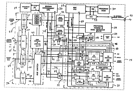
As illustrated in Fig. 2A, data communication
controller 15 of the present invention comprises a number
of major components, namely: a DMA Controller 25; Bus
Interface Unit 26; a Buffer Management CPU (BMC) 27 and
associated program ROM 28: a MAC CPU 29. and associated
program ROM 30; a Serial Communication Subsystem 31; dual-
WO 94/08308 PCT/US93/08985
17
ported RAM 32; communication register blocks 33; BMC
interrupt register blocks 34: MAC interrupt register block
35; protocol timers and miscellaneous register blocks 36;
transmit channel multiplexes (TX MUX) 37; receive channel
multiplexes (RX MUX) 38; and clock generator 39.
The DMA controller comprises a four channel DMA
Channel Address Unit 40, each DMA channel having an
external address counter, an internal address counter, a
byte counter and associated logic circuitry; an Address
FIFO 41; a Bus Interface Controller (BIC) 42; and a DMA
Control and Arbitor Unit 43. As shown, the Bus Interface
Unit also comprises a number of subcomponents namely: a
Data Input FIFO (DIN FIFO) 44; a Data Output FIFO (DOUT
FIFO) 45; and a bus switch 46 controllable by the DMA
Control and Arbitor Unit. Likewise, the Serial
Communication Subsystem comprises a number of
subcomponents, namely: a Transmit FIFO 47, a Transmit
Arbitor 48, a Transmit FIFO Input Multiplexes 49, and a
Packet Transmission Machine 50 along the transmit channel;
and a dual-port R~=_ceive FIFO 51, a MAC Receive Packet
Filter 52, a BMC Receive Packet Filter 53, and a Packet
Reception Machine 54 along the receive channel of the
subsystem; and a Token Control Unit 55.
As illustrated in Fig. 2A, the BMC has a program
instruction fetch bus 56 operably connected between
program ROM 28 and BMC in order to fetch program
instructions, whereas a separate program instruction
execution bus (comprising data lines 57 and address and
control lines 58) is provided to operably associate the
BMC with DMA Channel Address Unit 40, DMA Control and
Arbitor Unit 43, Transmit Channel Multiplexes 37, Receive
Channel Multiplexe~r 38, Packet Transmission Machine 50,
BMC Interrupt Register Block 34; Communication Register
Block 33, and Dual.-ported RAM 32.
In the illustrative embodiment, Address FIFO 41 has a
depth of three with each address location having a width
WO 94/08308 PCT/US93/08985
~~.'~ 44~a
18
of 24 bits and seven (7) tag bits associated with each
address. As illustYated, both the insert and removal
locations in the Address FIFO are specified by insert and
removal pointers 60 and 61 generated by BIC 42. As shown,
the addresses generated from DMA Channel Address Unit are
provided to the insert location of the Address FIFO,
whereas the tag bits provided to the insert location
thereof are generated by the DMA Control and Arbitor Unit.
The particular functions which these DMA channel tags
serve will be described in greater detail hereinafter.
As illustrated in Fig. 2A, DIN FIFO 44 and DOUT FIFO
45 each have a depth of three with the word location of
each FIFO being 16 bits. The DIN FIFO has five (5) tag
bits associated with (i.e. attached to) each word read
using the address originally associated with the tag bits
in the Address FIFO. The insert and removal locations in
DOUT FIFO are specified by insert and removal location
pointers 60 and 61, which are simultaneously generated by
the BIC when generating the removal and insert pointers
for the Address FIFO. The insert and removal locations
in DIN FIFO are specified by insert and removal location
pointers 62 and 63 generated by the BIC.
The entry location in the DIN FIFO and the removal
location in the DOUT FIFO are connected to the lines of
system data bus 64, whereas the removal location in the
Address FIFO is connected to the lines of system address
bus 65. Data word bits in the removal location of the DIN
FIFO are provided to data bus 66 which extends into Bus
Switch 46. The tag bits of the removal location in the
DIN FIFO are provided to the DMA Control and Arbitor Unit
by way of lines 67. The data word bits from the Receive
FIFO are eventually provided to the insert location in the
DOUT FIFO by way of bus 68 extending from Bus Switch 46.
System control signals and control attention (CA) signal
are provided to BIC over control lines 69 and 70, whereas
WO 94/08308 ~ ~ ~ ~ ~ ~ ~ PCT/US93/08985
19
the Interrupt (INT) Signal is provided by the BIC to the
host processor over line 71.
As will be described in greater detail hereinafter in
connection with F'ig. 2B, a number of signals are
transmitted between the DMA Control and Arbitor unit and
the BMC to generate INT and other system control signals.
Also, control signals are generated by the DMA Control and
Arbitor unit so as to arbitrate among the four DMA
Channels according to a preselected arbitration scheme.
As illustrated in Fig. 2A, a first unidirectional
data bus 72 extends between Bus Switch 46 and one input
port of transmit channel multiplexes 37, whereas a second
unidirectional data bus 73 extends between one output port
of receive channel multiplexes 38. Control line 74
extends from the DMA Control and Arbitor Unit to
multiplexes 37 to selectively switch between data bus 72
or BMC data bus 57. The output of multiplexes 37 is
connected to one input port of input Transmit FIFO
multiplexes 49 by way of a third data bus 76, whereas one
output port of Receive FIFO 51 is connected to the input
port of multiplexes 38 by way of a fourth data bus 77.
Control line 75 permits multiplexes 38 to selectively
switch between data buses 57 and 73.
In order to generate interrupts to the BMC upon the
occurrence of particular events within the data
communication controller, BMC interrupt Register Block 34
contains a plurality of interrupt signal sources, into
which flags can be set by the DMA Control and Arbitor
Unit. The BMC Receiver Packet Filter, the Transmit FIFO
Arbitor and the Packet Transmission Machine using lines
78, 79, 80 and 81,, respectively. Flags set in BMC
Interrupt Register Block 35 can be read by the BMC and the
DMA Control and Arbitor Unit over data bus 57, while BMC
interrupts are provided to the BMC over interrupt line 82
as shown. Similarly, interrupt flags can be sent in CPU
Interrupt Register Block 35 by the Packet Transmission
WO 94/08308 PCT/US93/08985
~1~4~~
Machine, the Transmit Arbitor, the MAC Receiver Packet
Filter, and Protocol Time Register Block 36 over lines 83,
84, 85 and 86, respectively. BMC Interrupts are sent
over line 87 to the MAC CPU.
5 As illustrated in Fig. 2A, the MAC CPU has a program
instruction fetch bus 88 operably connected between
program ROM 30 and MAC CPU in order to fetch programs
instructions. Also, a separate program instruction
execution bus (comprising data lines 89 and address and
10 control lines 90) is provided to operably associate the
MAC CPU with dual-ported RAM 32, Communication Register
Block 33, Packet Reception Machine 31, MAC Receiver Packet
Filer 52, Transmit Arbitor 48, multiplexes 49 Packet
Transmission Machine 50, MAC Interrupt Register Block 35,
15 and Protocol Timers and Miscellaneous Register Block 35,
as shown.
As shown in Fig. 2A, a programming port 91 is
provided in the data communication controller in order
that external program memory (RAM or ROM) may be
20 accessible to the MAC CPU by way of multiplexes 92. In
this way the MAC layer protocol can be simply changed from
application to application as desired.
As the MAC CPU is not capable of accessing shared
memory 21, various parameters destined for the MAC CPU are
first written by the host system into shared memory and
then accessed by the BMC, which stores them into RAM 32 or
Register 33. Thereafter, this data can be subsequently
accessed to the MAC CPU. To achieve such tasks, a
communication pathway is provided between the BMC and the
MAC CPU using Dual-port RAM 32 and Communication Register
Block 33, which are operably connected between the program
instruction execution buses 57 and 89 of the BMC and MAC
CPU, respectively. Thus, for example, using dual-ported
RAM 32, the MAC CPU can communicate directly with the BMC,
and using the Communication Register Block 33, the MAC CPU
can communicate indirectly with the host system.
WO 94/08308 c~ f , ~ PCT/US93/08985
21«-~:~.i2
21
Parameters relating to MAC layer protocol timing and
related functions. are stored in the Protocol Timers and
Miscellaneous Register :Block, and are accessible to the
MAC CPU by way of program instruction execution bus 89.
In the illustrative embodiment, Transmit FIFO 47 has
a depth of 16 storage locations, with each storage
location having a width of 18 bits, 16 bits for data words
and 2 associated tag bits for indicating the location of
data within words and the packet boundaries which is
highly advantageous for packet assembly at the packet
transmission machine. The specific types of tag bit
sequences will be described in greater detail hereinafter.
As illustrated, the insert location (i.e. port) in the
transmit FIFO is specified by an insert located pointer 93
generated by the 'Transmit Arbitor. The output port of
transmit FIFO input multiplexes 49 is connected to the
data word insert .location in the transmit FIFO to transfer
data words thereto, whereas the tag bits are provided to
the tag bit insert location in the transmit FIFO. As will
be described in greater detail hereinafter, the specific
values of the transmit FIFO tag bits are decided by the
BMC using Write T:K_FIFO-TAG flags sent over
address/control bus 58 to the Transmit Arbitor stored
therein, and eventually written as TX_FIFO-Tag bits in the
transmit FIFO. A:~ will be explained in greater detail
hereinafter, the primary function of the Transmit Arbitor
is to give either the MAC CPU or BMC control over the
transmit channel.
The removal location in the Transmit FIFO is specific
by removal location pointer 94 specified by the Packet
Transmission Machine. The data word bits and the
TX-FIFO tag bits j:rom the removal location of the transmit
FIFO are provided to separate input ports in the Packet
Transmission Machine and processed in a manner to be
described in greater detail hereinafter. The primary
function of the Packet Transmission Machine is to utilize
WO 94/08308 PCT/US93/08985
~~~:'-~e~~
22
the TX FIFO TAG bits to assist in the assembly of packets
transmitted under the control of the BMC or MAC CPU. The
output of the Packet Transmission Machine is a serial bit
stream provided over the TXD line as output to
communication medium interface unit 22, with clock signals
over the MRCLK line in a manner well known in the art.
In the illustrative embodiment, Receive FIFO- has a
depth of 32 storage locations, each storage location
having a width of 17 bits, 16 bits for a data word, and
one (1) tag bit (i.e. RX_FIFO TAG BIT) associated with
each received data word. As will be described in greater
detail hereinafter, to the function of the FX-FIFO TAG
bits is to indicate which words belong to a received
packet, so that a number of received packets, each of
variable length, can be buffered in the Receive FIFO,
thereby increasing data throughput. The insert location
of the Receive FIFO is specified by a input pointer 95
generated from Packet Reception Machine. Words of data
received from the Packet Reception Machine are provided to
the 16 bit locations in the input port (i.e. insert
location) of the Receive FIFO, while the RX_FIFO TAG bit
is provided to the tag bit location by the Packet
Reception Machine. The bit input line RXD, the clock line
RXCLK and other signals from communication medium
interface unit 22 are provided to the input port of the
Packet Reception Machine in a manner well known in the
art.
To provide both the MAC CPU and the BMC access to
MAC-packets and Non-MAC packets, the Receive FIFO has two
independent output ports, with the 16 data bit locations
of output port A operably associated with data bus 89,
while the 16 data bit locations of output port B are
operably associated to data buses 57 and 73. As shown,
the removal location of output port A is specified by an
output pointer 96 generated from within the MAC Receiver
Packet Filter, whereas the removal location of output port
WO 94/08308
PCT/US93/08985
23
B is specified by an output pointer 97 generated from
within the BMC Rs:ceive Packet Filter. Also, the tag bit
location from output port A is provided as input to the
MAC Receive Packed Filter, whereas the tag bit location
from output Port B is provided as input to the BMC Receive
Packet Filter. As will be described in greater detail
hereinafter, packets can be independently processed within
the MAC and BMC F:eceive Packet Filters and interrupts
generated to the BMC and MAC Interrupt Register Blocks
upon the detection of either a MAC-packet or NON-MAC
packet in the Receive FIFO. To facilitate such processes,
output port A of the Receive FIFO is operably connected to
an input port of MAC receive packet filter, and output
port B of the Receive FIFO is operably connected to an
input port of BMC receive packet filter. In this way,
words associated with received data packets can be
"scanned" and analyzed while in the Receive FIFO using
RX-FIFO TAG bits to determine the beginning and ending of
received packets. The primary function of the MAC Packet
Filter is to determine whether a received packet is a
particular type of MAC-packet, in which case an interrupt
flag is written into the MAC interrupt Register. This
will indicate to the MAC CPU that a particular MAC packet
is on data bus 89 for processing in accordance with the
MAC layer protoco:L. The primary function of the BMC
Receive Packet Fi:Lter is to determine whether a received
packet is for the BMC and free of error. If so, the BMC
Receive Packet Fi:Lter passes control over the reception
process to the BMC, which in turn routes the received
packets) through bus switch 46, DOUT FIFO 45, until
eventually the received packets are stored within either a
MAC-PACKET Receive: Queue or a NON-MAC PACKET Receive Queue
maintained within the shared buffer memory. The exact
operations which are performed within the data
communication controller of the present invention will be
described in greater detail hereinafter.
WO 94/08308 PCT/US93/08985
21~~~~~'
24
In Fig. 2B, the major subcomponents of the BIC are
illustrated in greater detail. As illustrated, the BIC
comprises a Bus Interface Signal Receiver/Generator and
Bus State Control Unit 100, a DIN FIFO Control Unit 101
and an Address FIFO/DOUT FIFO Control Unit 102. The
primary function of Unit 100 is (1) to detect Control
Attention (CA) signals from the host system and other
system control signals on the system bus; (2) to control
the flow of data between the system bus and the internal
buses within the data communication controller; and (3) to
generate Control Command Busy (CBSY) and Interrupt (INT)
signals to the host and other system control signals to
the system bus.
As illustrated in Figs. 2A and 2B, four primary
control signals are passed between the BIG and the DMA
Control and Arbitor Unit. The AF_IN-RDY signal passed
from the Address FIFO/DOUT FIFO Control Unit to the DMA
Control and Arbitor Unit indicates that the Address FIFO
is ready for address input from DMA Address Block 40 and
for Address-FIFO TAG bit input from the DMA Control and
Arbitor Unit. The AF OUT RDY signal indicates that the
Address FIFO contains an address in its removal location.
The AF WR signal provides the insert location pointer for
the Address FIFO and DOUT FIFO, whereas the AF RD signal
provides the removal location pointer for the ADDRESS FIFO
and the DOUT FIFO. The WR AF signal controls the writing
of address and tags bits into the insert location of the
Address FIFO, as well as the writing of data from the
Receive FIFO or BMC data bus 57 into the insert location
of the DOUT FIFO. The RD AF signal controls the reading
of address bits from the removal location of the Address
FIFO onto the system address bus, as well as the reading
of data bits from the removal location of the DOUT FIFO
onto the system data bus.
The DIN OUT RDY signal indicates that the DIN FIFO is
ready to output data from the removal location of the DIN
WO 94/08308 PCT/US93/08985
FIFO to the ins~:rt location of the Transmit FIFO or to the
BMC instruction execution BMS through the Bus Switch 46.
DIN_IN READY indicates that the DIN FIFO is ready for data
input from the shared buffer memory to the insert location
5 in the DIN FIFO. The DIN WR signal provides the insert
location pointer for the DIN FIFO, whereas the DIN RD
signal provides t:he removal location pointer for the DIN
FIFO. The WR DIN signal controls the reading of address
tag bits from the removal location of the Address FIFO to
10 the tag bit insert location in the DIN FIFO and controls
the writing of a data word from the shared buffer memory
to the insert location in the DIN FIFO. Finally, the
RD DIN signal controls the reading of a data word from DIN
FIFO to the insert location in the Transmit FIFO or BMC
15 data bus 57.
In Fig. 2C, the subcomponents of the Receive FIFO and
the Receive Packet. Machine are illustrated in greater
detail. As shown in Fig. 2C, the Receive FIFO comprises
Receive FIFO cells 105, a Receive FIFO Input Pointer 106,
20 MAC Receive Output: Pointer 107, a BMC Receive FIFO Output
Pointer 108, a BMC: Receive Output Pointer Temporary Store
109, a MAC Receive: FIFO Output Register 110, and a BMC
Receive FIFO Output Register 111. Receive FIFO Cells 105
have insert and removal ports for data words, and insert
25 and removal ports for RX FIFO TAG bits, as indicated.
Address ports for insert and removal pointers are also
provided as shown.
In Fig. 2C, the subcomponents of the Packet Reception
Machine 54 are illustrated in greater detail. As shown,
the Packet Reception Machine comprises a Receive Clock
Buffering Circuit 112, a baud to bit converter 113, a
serial to parallel converter 114, a 16 bit holding
register 115, a SD/ED Detection Unit 116, a Receive CRC
Unit 117, a Receive Bit Control Unit 118, and a Receive
Byte Control/Receive FIFO Stuffing Unit 119 configured in
- a~manner as shown. The encoded serial data input stream
WO 94/08308 PCT/US93/08985
2~1~~~~~
26
of the RXD line is converted into bits by baud to bit
converter 113 in a conventional manner, and are loaded
into serial to parallel converter 114, in groups of 16
bits. The SD/ED detection unit 116 senses the bits as
they are received and sends SD and ED detection signals to
Receive Bit Control Unit 118. Simultaneously, CRC error
detection is performed at RX CRC Unit 117, which provides
to the Receive Bit Control Unit 118, error information
regarding each sequence of bits being loaded into the
holding register. The Receive Bit Control Unit, in turn,
provides the SD/ED detection data and CRC information to
the Receive Byte Control/Receive FIFO stuffing unit, which
determines and remembers which words loaded into the
holding register are associated with which received data
packets. Preferably, the Receive Byte Control/Receive
FIFO stuffing unit is realized as a non-finite state
machine constructed from a Programmable Logic Array (PLA)
and associated logic circuitry, so that more than one
state, in the multistate packet reception process can be
held (i.e. tracked) during the packet reception on a real-
time basis. A primary reason why a Non-Finite State
machine is desirable in the packet reception process is
due primarily to the fact that the length of any incoming
packet may virtually any length, which means any number of
words may comprise each received packet.
The primary task of the packet reception machine is
to (1) determine which received words belong to which
received packets; (2) what the length of each received
packet is; (3) what the (error) status of each packet is;
and (4) to write (i.e. stuff) status and packet length
words along with RX-FIFO-TAG bit of value 1 in the Receive
FIFO, behind the last word of a packet. In this way, the
MAC and BMC Receive Packet Filters can separate one
received packet from another, determine its type and then
permit it to be transferred to its destination for
processing.
WO 94/08308 PCT/US93/08985
27
As illustrai:ed in Fig. 2C, the WR WORD signal to the
holding register is generated by the Receive Bit Control
Unit over line 120 and controls the writing of 16 data
bits into the Holding Register. The WR RX-FIFO signal to
the Holding Register is generated by the Receive Byte
Control Unit over line 121 and controls the writing of the
16 bit data word from the Holding Register to the insert
location (i.e. port) of the Receive FIFO cells. The
WR RX FIFO signal. is also provided to Receive FIFO Pointer
106 and the BMC receive Packet Filter to keep track of the
FIFO status. The WR_RX TAG signal provided to the TAG
insertion port, is also generated by Unit 119 in order to
write RX-FIFO TAG for the packet status and packet length
words loaded into the input port of the Receive FIFO under
the control of Unit 119. After the last word of a
received packet has been written into the Receive FIFO,
Unit 119 writes, in parallel, into the insert port of the
receive FIFO, a 16 bit status word (and a tag bit equal to
1) associated with the received packet, and after the
words in the FIFO have been advanced forward, writes a 16
bit Packet Length Word (and a tag bit equal to 1) into the
next FIFO insert .location.
As illustrated in Fig. 2C, the word and tag bit
locations of the :removal port of the Receive FIFO are
operably connected to corresponding locations in the
Receive FIFO Output Register. The address of removal port
A is specified by MAC Receive FIFO Pointer 107, which is
incremented by the INC MAC OPTR signal generated by the
MAC CPU Receive Packet Filter 52. The tag bits from the
removal port of the Receive FIFO are also provided to the
MAC CPU Receive Packet Filter over line 122. Words and
tag bits at the removal port of the Receive FIFO are
automatically provided to the word and tag Bit locations
of the MAC Receive: FIFO Output Register. In this way, the
FC field of each packet in the Receive FIFO can be read by
the MAC CPU Receive Packet Filter so as to determine
WO 94/08308 PCT/US93/08985
whether the received packet is a MAC packet destined for
the MAC CPU. The output of the MAC Receive FIFO Output
Register is connected to bus 89, and the reading words
from the output register and the MAC CPU bus is controlled
by READ MAC Reg signal provided from the MAC CPU.
Similarly, the word and tag bits from removal port B
of the Receive FIFO are automatically provided to the word
and tag bit locations of the BMC Receive FIFO Output
Register so that the FC field of packets and RX-FIFO TAG
bits in the Receive FIFO can be easily read to determine
whether a received packet is destined for the BMC. The
output of the BMC Receive FIFO Output Register is
connected to the input of multiplexer 38, and the reading
of words from the output register and onto the BMC bus is
controlled by the READ-BMC REG signal provided from the
DMA Control and Arbitor Unit. The RX-FIFO TAG bits from
the BMC Receive Packet Filter are provided to the BMC by
way of BMC address/control bus 58.
The operation of the MAC Receive Packet Filter will
be described with reference to the flow chart of Fig. 2D.
Upon the resetting of the data communication controller
(i.e. after power-up), the automatically enters Block A in
Fig. 2D and periodically incrementing MAC OUTPUT OPTR.
While doing so, the MAC Receive Packet Filter reads tag
and data bits from the MAC Receive FIFO output register,
and analyzes them to determine whether a MAC-Packet (i.e.
frame) is received. As indicated at Block B, when a MAC-
Packet is detected (i.e. MAC-FRAME Signal is set), the MAC
Receive Packet Filter issues a MAC RX GO sign to the MAC
CPU. At Block C, the MAC CPU takes control over the
removal Port A of the Receive FIFO (i.e. periodically
reads MAC Receive FIFO register which automatically
increments the MAC OPTR), and processes, e.g. parses, the
MAC packet. At Block D, the MAC Receive Packet Filter
determines whether the MAC CPU detects a Receive FIFO
"Flush," condition. If so, it then determines Block E
WO 94/08308 PCT/US93/08985
~~?!~~~ i?
29
whether the MAC C':?':' generated a FLUSHPASS TAG or a
FLUSH TILL TAG. If a FLUSH TILL TAG is generated, then
the MAC Receive Packet Filter regains control over removal
port A of the Receive FIFO, flushes (i.e. erases data and
tag bits from) th.e Receive FIFO up to but not beyond the
position of the t.ag in the Receive FIFO, and thereafter
issues a FLUSH DONE Signal to the MAC CPU. At this stage,
the MAC Receive Packet Filter returns to BLock C and
continues the process. If, however, at Block E, the MAC
CPU generates a FLUSHlPASS TAG, then at Block F, the MAC
Receive Packet Filter regains control over the removal
port of the Receive FIFO, flushes the Receive FIFO past
the tag in the MAC Receive FIFO output Register, and then
issues a FLUSH DONE Signal to the MAC CPU.
If at Block :D, the MAC CPU did not detect a Receive
FIFO Flush Condition, then at Block G, it determines
whether the MAC C:PU detects the end of a packet (i.e. a
tag bit set in tha_ MAC Receive FIFO output Register). If
not, the process :returns to Block C. If, however, an End
of Packet Tag bit is detected, the MAC CPU at Block H
finishes processing the end of the packet and then the MAC
Receive Packet Filter regains control over removal port A
of the Receive FIFO.
The operation of the BMC Receive Packet Filter will
be described with reference to the flow chart of Fig. 2E.
Upon resetting of the data communication controller,
as described above:, the BMC receive packet filter enters
Block A. At this block, and while periodically
incrementing BMC-OPTR, the BMC Receive Packet Filter reads
tag and data bits from BMC receive output register, and
analyzes them to determine whether a BMC packet has been
received and also whether four words have been loaded into
the receive FIFO. As indicated at Block B, when a BMC
packet is detectedl (i.e. BMC_Packet signal set) and four
words have been received and loaded into the Receive FIFO,
the BMC Receive Packet Filter saves the pointer at the
WO 94/08308 PCT/US93/08985
~1~~='~~~ 30
removal port B (i.e. BMC-OPTR), and stores it in
Temporary Store 109. At Block C, the BMC receive packet
filter increments BMC OPTR by 1, checks the tag at
removal port B of the Receive FIFO to determine whether
the tag is set to 1 (i.e. packet terminated condition),
and uses the previously stored words in the Receive FIFO
to check whether error conditions are present during the
packet reception process. As indicated at Block D, the
BMC Receive Packet Filter proceeds to Block E if either
the tag bit at removal port B is equal to 1 or there is an
error detected in the received packet. At Block E, the
BMC Receive Packet Filter restores the BMC Receive FIFO
output pointer stored in Temporary Store 109. At Block F,
the BMC Receive Packet Filter flushes the Receive FIFO
past the two words with a tag bit value equal to 1 in BMC
Receive FIFO Output Register 111, and thereafter returns
to Block A, to repeat the process.
If, however, at Block D, the tag bit at removal port
B of the Receive FIFO is not equal to 1 and no error
conditions have been detected in the receive packet, then
at Block G, the BMC Receive Packet Filter determines
whether the pointer at removal port B has been shifted up
to three address value from the stored removal port B
pointer (i.e. Saved- BMC_ OPTR). If not, the BMC
Receive Packet Filter returns to Block C. However, if it
has been shifted up to three address values, then the BMC
Receive Packet Filter proceeds to Block H. At Block H,
the BMC Receive Packet Filter restores BMC receive FIFO
output pointer stored in Temporary Store 109, and issues
the BMC-RX GO signal to the BMC. At Block I, the BMC
Receive Packet Filter passes control over removal port B
of the Receive FIFO to the BMC for the duration of the
data packet reception process. At Block J, the BMC
Receive Packet Filter determines whether any error
conditions are detected in the received packet. If there
are error conditions present, then the BMC Receive Packet
WO 94/08308 PCT/US93/08985
~1~~~ ~~
31
Filter flushes the Receive FIFO past the two words with
tag bits equal to 1 in the BMC Receive FIFO Output
Register, and thereafter returns to Block A.
If, however,,~at Block J no error conditions are
present in received packet and data packet reception
process is not completed by the BMC (i.e. BMC RX DONE
signal is not set.), the BMC Receive Packet Filter returns
to Block J. When the data packet reception process is
completed, at Block L the BMC Receive Packet Filter
regains control over removal port B of the Receive FIFO
and continues analyzing tag and data bits in the BMC
Receive FIFO Output Register, returning to Block A to
close the loop of the filtering process.
In Fig. 2F, the subcomponents comprising Transmit
Arbitor 48 are shown. As illustrated, the Transit Arbitor
comprises Transmit Arbitor Control Unit 125, Priority Bit
Comparator 126, BMC Transmit Access-Class Register 127,
any Bit Detector 128, BMC Address Decoder 129, Any Bit
Detector 130, MAC Transmit Access-Class Register 131, and
MAC Address Decoder 132. As illustrated, BMC data bus 57
is connected to the input of the BMC Transmit Access-Class
Register and provides eight (8) BMC transmit access-class
bits to this register. As will be described in greater
detail, these eight bits are read by the BMC from the
System Control Block (SCB). The Resume Control Word is
written into the ,SCB by the host system to indicate to the
data communication controller that it may resume packet
transmission when it is ready and able to do so. Each of
these eight BMC priority bits represents the priority of
each Access-Class Transmit Queue stored in shared buffer
memory, from which packets are sought to be transmitted
through the transmission channel of the communication
controller. The output of the BMC Transmit Access-Class
Register is provided to port A of the Priority Bit
Comparitor, while Detector 128 is adapted to detect
whether any bit i:a present in the BMC Transmit Access-
WO 94/08308 PCT/US93/08985
~1~4~~~
32
Class Register. If so, Bit detector 128 issues a
BMC TX Packet RDY signal to the Transmit Arbitor
Control Unit.
As indicated in Fig. 2F, MAC data bus 89 is connected
to the input of the MAC Transmit Access-Class Register and
provides MAC transmit access class bits to this register.
These bits are provided by the MAC CPU and represent the
priority of the MAC CPU in accessing the transmit channel
at any particular instant within the MAC layer protocol.
The output of the MAC Transmit Access-Class Register is
provided to port B of the Priority Comparitor, while Bit
Detector 130 is adopted to detect whether any bit is
present in the MAC Transmit Access-Class Register. If so,
Bit Detector 130 issues a MAC TX-PACKET- RDY signal to
the Transmit Arbitor Control Unit. The function of the
Priority Bit Comparator is to compare the BMC priority
access bits (A) against the MAC priority access bits (B)
when BMC-TX-PACKET RDY and MAC TX-PACKET RDY signals
are set to 1. If A is greater than B, then the Priority
Bit Comparator issues BMC>MAC=1 signal to the Transmit
Arbitor Control Unit. If, however, A<B, then the Priority
Bit Comparitor issues a MAC>BMC=1 signal to the Transmit
Arbitor Control Unit.
At any instant in time, the BMC and/or the MAC CPU
may desire to access the transmission channel. In the
case when the BMC desires to set DMA Channel 2, which
controls the transmission channel during the packet
transmission process, the BMC must first compete against
the MAC CPU to gain control over the transmission channel
and then delegate its acquired control to the DMA Arbitor
and Control Unit. There will be, however, instances when
the BMC, rather than the DMA Control Unit, needs to
control the transmission channel, such as when aborting
the transmission of data packets in the Transmit FIFO.
There will also be times during the MAC layer protocol,
when the MAC CPU needs either conditional or unconditional
WO 94/08308 PCT/US93/08985
~~?~~'-~ a?
33
access to the transmission channel. In any of these
instances of transmission channel access, the BMC, DMA
Channel 2 and the MAC CPU need to (indirectly) write
transmit tags into the Transmit FIFO as data words are
being written thereinto. Consequently, the BMC can send
control signals over the BMC address control bus, which
when decoded in BMC Address Decoder 129, results in
commands BMC-WR_ TX TAG-1 and BMC-WR TX TAG O being
sent to the Transmit Arbitor Control Unit so that it will
write a BMC-selected pair of tag bits into the Transmit
FIFO. Similarly,, the MAC can send control signals over
the MAC address/c:ontrol bus which when decoded by MAC
Address Decoder 132 results in commands MAC WR TX TAG 1
and MAC WR TX- TAG-O being sent to the Transmit Arbitor
Control Unit so that it will write a MAC-selected pair of
tag bits into the' Transmit FIFO. Also, when DMA Control
Unit access over the Transmit FIFO, it too can send
commands DMA WR TX TAG 1 and DMA WR TX TAG 0 to the
Transmit Arbitor Control Unit so that it will write a DMA-
selected pair of tag bits into the Transmit FIFO. In the
illustrative embodiment, possible sequences of transmit
tag bits (i.e. T~S_FIFO TAG-) are as follows:
00 Write TX word
01 Write TX BYTE
10 Write TX last word
110 Write ~TX last Byte
111 Write -TX- abort,
where the first two bits are written in the tag bit
locations and the third bit is written into the least
significant bit (LSB) of the lower field of the 16 bit
data word in the Transmit FIFO. In essence, these
transmit FIFO tag bits are instructions to the Packet
Transmission Machine specifying (i) the boundary of the
transmit packets, (ii) the position of data bytes within
the associated word, and (iii) what to do with such data
during the packet assembling and transmission process.
WO 94/08308 PCT/US93/08985
~~~e 5~
34
Specifically, transmit FIFO tag sequence 00 indicates that
all 16 bits in the attached data word should be packeted
and transmitted. Transmit FIFO tag sequence O1 indicates
that only 1 data byte is contained in the upper field of
the attached data word and that this byte is to be
packeted transmitted. Transmit FIFO tag sequence 10
indicates that the 16 associated data bits are represented
by the last word in the packet and should be packeted and
transmitted. Transmit FIFO tag sequence 110 indicates
that the last data byte is located at the upper field in
the attached data word and that this byte should be
packeted and transmitted. Lastly, transmit FIFO tag
sequence 111 indicates that the entire packet should be
discarded and an ABORT sequence should be transmitted by
the TX_machine. When a particular bit sequence is
requested to be written and granted, the actual process of
writing (or aborting) these bits sequences occurs using
signals these which are provided to the Transmit FIFO, as
shown in Fig. 2G.
There are a number of other significant control
signals which the transmit arbitor control unit considers
before either the MAC CPU or BMC is granted control (i.e.
"ownership") over the entire transmission channel. The
signal which indicates which control processing unit has
control over the transmission channel is indicated by
MAC_OWN TX, which if 1 indicates that the MAC CPU
controls it, and if 0 indicates that the BMC owns it. The
control signal which indicates the MAC CPU's unconditional
demand for the transmission channel is GET TX, whereas
FLAG_GET TX is a flag sent to the BMC to indicate that
its control over the transmission channel has been taken
away by the MAC CPU. If the BMC acknowledges
FLAG_GET TX by setting flag ACK MAC GET TX, in
response thereto, the MAC CPU will automatically return
control over the transmission channel to the BMC when the
MAC CPU has finished using it.
WO 94/08308 PCT/US93/08985
The arbitration process for the transmission channel
is controlled by logic circuitry implemented with Transmit
Arbitor Control LJnit. This logic circuitry is described
by the five (5) ::ets of Boolean equations set forth in the
5 table of Fig. 26. Boolean equation set (1) describes
under what conditions the FLAG GET TX flag is sent to
the BMC, and under what condition the F1AG is cleared by
the BMC. This flag is important to the channel
arbitration process, as it permits the BMC to logically
10 resume its operations after the transmission channel has
been taken away by the MAC CPU. Boolean equation set (2)
describes under what condition the MAC CPU controls (i.e.
owns) transmission channels and under what conditions it
does not. Boolean equations set (3) describes under what
15 conditions a BMC__ Request TX is sent to MAC interrupt
register block 34, and under what conditions a
MAC~Request TX is sent to BMC Interrupt Register Block
34. Boolean equation sets (4) and (5), respectively,
describe under what condition the MAC CPU controls the
20 transmission channel and under what conditions the BMC
controls the transmission channel. These Boolean
expressions can be utilized to implement the logic
circuitry of the '.transmit Arbitor Control Unit in a
straightforward manner.
25 Fig. 2H illu:~trates the interrupt routine performed
by the MAC CPU when passing transmission channel control
to the BMC. As illustrated, when BMC-Request TX=1, the
MAC CPU is interrupted. In servicing this interrupt, the
MAC CPU issues in:atructions through MAC address/control
30 bus 90 to the MAC Address Decoder 132, which generates the
signal GIVE TX TO-BMC=1 to the Transmit Arbitor Control
Unit, which in turn sets flag MAC OWN-TX=0, thus passing
control over the transmission channel to the BMC.
Thereafter, the MI?,C CPU returns from the interrupt and
35 resumes its tasks according to MAC layer protocol.
WO 94/08308 PCT/US93/08985
36
Fig. 2I illustrates the interrupt routine performed
by the BMC when passing transmission channel control to
the MAC CPU. As illustrated, when MAC- Request TX=1,
then the BMC is interrupted. In servicing this interrupt,
the BMC issues instructions through BMC address/control
bus 58 to BMC Address Decoder 129, which generates the
signal GIVE TX TO MAC=1 to the Transmit Arbitor Control
Unit, which in turn sets flag MAC OWN TX=1, thus passing
control over the transmission channel to the BMC.
Thereafter, the BMC returns from the interrupt and resumes
its tasks.
In Fig. 2J, the subcomponents of Transmit FIFO 51 are
shown. As shown, the Transmit FIFO comprises Transmit
FIFO cells 134, Input Pointer 136, Output Pointer Decoder
137, Output Read Pointer 138, and Transmit FIFO Control
Unit 139. As shown, the 16 data lines from the output
port of multiplexer 49 are connected to the 16 bit
locations at the insert location of transmit FIFO Cells
134. In order to utilize bit-0 of this bus for writing
Transmit Abort bit sequences (i.e. 111) as described
above, an OR gate 140 is inserted in the bit-0 data line,
as shown, so that the output of the OR gate is connected
to the bit 0 in the insert location of the transmit
FIFO, while the WR-TX ABORT line from the Transmit
Arbitor Control Unit is one input to the OR gate while the
bit-0 line from input multiplexer 49 is the other input
thereto. The two TX FIFO TAG lines are connected to the
two tag bit locations in the insert location of the
Transmit FIFO.
As illustrated in Figs. 2J and 2K, the 16 bit
TX FIFO OUT BUS lines from the removal location of the
Transmit FIFO are connected to the 16 bits of the insert
location of Transmit synchronizing FIFO 142 of the Packet
Transmission Machine. The two TX-FIFO OUT TAG lines
from the removal location of the Transmit FIFO are
connected to the two tag bits of the insert location of
WO 94/08308 PCT/US93/08985
21~~~~~~
37
the Transmit Synchronization FIFO. The WR TX FIFO lines
from the Transmit. Arbitor Control Unit is connected to the
Transmit FIFO Control Unit to control writing of bits and
tags into the Transmit FIFO, whereas the
TX-FIFO_INPUT_ RDY line is sent back to the Transmit
Arbitor Control Cfnit to advise that the Transmit FIFO is
ready to be written into. The WR TX FIFO line is
connected to Input Write Pointer 136 in order to control
the insert pointer to the Transmit FIFO cells
As illustrated in Figs. 2J and 2K, the READ TX FIFO
line is connected. from Transmit Byte Control Unit 143 to
the Transmit FIFO Control Unit to advise that the Packet
Transmission Machine is ready to read a word and tag bits
from the Transmit FIFO. The read-TX-FIFO line is also
connected to Output Read Pointer 138 to control the
removal location pointer in the transmit FIFO. The TX-
FIFO-OUTPUT-RDY line from the transmit FIFO is connected
to Transmit Byte Control Unit 143 to advise that the
Transmit FIFO is ready to output word and tag bits to the
Transmit Synchronization FIFO.
As illustrated in Fig. 2K, the Packet Transmission
Machine comprises a number of major subcomponents, namely:
Transmit Byte Control Unit 143, Transmit Bit Control Unit
144, MAC/BMC Bus Multiplexer 145, First Multiplexer 146,
Transmit Parallel-In-Serial-Out (PISO) Converter 147,
Transmit CRC Generator 148, Second Multiplexer 149, Bit-
Code-To-T-Code Converter 150, Third Multiplexer 151, and
T-Code To Differential Manchester Code Converter 152. In
the illustrative Eambodiment, the depth of transmit
synchronization FIFO is four (4), with each word location
having a width of 16 bits and each attached tag location
having a width of 2 bits.
As the primary function of the packet transmission
machine is to perform packet and token generation
procedures, the machine must know which central processing
unit (CPU) controls the transmission channel at each
WO 94/08308 PCT/US93/08985
38
instant in time. This is achieved by providing the MAC-
OWN-TX line from the Transmit Arbitor Control Unit to the
Transmit Byte Control Unit. Whichever central processing
unit controls the transmission channel, it is capable of
issuing "transmit packet commands" over its system bus, to
the Transmit Byte Control Unit. To facilitate this
transmit command delivery process, the MAC, the BMC and
data and address/control buses are selectively connected
to the Transmit Byte Control Unit through Bus Multiplexer
145, using the MAC-OWN-TX line to provide a bus selection
control signal.
In order to advise the Transmit Arbitor Control Unit
that the packet transmission machine is busy, a TX-
Machine-Busy line is connected from the Transmit Byte
Control Unit to the Transmit Arbitor Control Unit. In
order to advise the BMC that its transmit packet command
has been executed, a MMC-TX-CND-Done line is connected
from the Transmit Byte Control Unit to the BMC Interrupt
Register Block. Similarly, to advise the MAC CPU that its
transmit packet command has been executed, a MAC-TX-CMD-
Done line is connected from the Transmit Byte Control Unit
to the CPU Interrupt Register Block.
Once the Transmit Byte Control Unit receives a
transmit packet command from either the MAC CPU or BMC, it
then begins to read data from the Transmit FIFO into the
Transmit Synchron- ization FIFO, and then uses the tags to
determine packet boundaries and then performs the IEEE
802.5 Standard. To achieve the packet assembly and
transmission process, the insert location of the Transmit
Synchronization FIFO is specified by an insert location
pointer generated by the Transmit Byte Control Unit. The
removal location of the Transmit Synchronization FIFO is
specified by the Transmit Bit Control Unit. The Transmit
Byte Control Unit is adapted to read the tag bits from the
Transmit Synchronization FIFO so that it can determine
where data bytes reside in the buffered words for purposes
WO 94/08308
PCT/ US93/08985
~1~~ ~~~?
39
of packet assembly. On the basis of detected tag bits,
packet assembly commands are issued from the Transmit Byte
Control Unit to the Transmit Bit Control Unit for
execution. The execution of these packet assembly
commands involves the Bit Control Unit selectively reading
bytes from the removal location of the Synchronization
FIFO, passing these bytes are passed through Multiplexer
146, to the Transmit PISO Unit, along with SD, ED and
other bits from Token-Ring Control Block 55. This packet
assembly process occurs under the control of Transfer Bit
Control Unit.
In the illustrative embodiment, the Transmit Byte
Control Unit is implemented as a Programmable Logic Array
(PLA) with subroutine and interrupt capabilities. The
Transmit Bit Control Unit is implemented by a Finite-State
Machine performing the IEEE 802.5 Standard. In accordance
with the token-ring packet format set forth in the IEEE
802.5 Standard, the 32 bit cyclic redundancy check (CRC)
sequence is generated by Transmit CRC Generator 148, and
is then inserted behind the information field using
Multiplexer 149 under the control of the Transmit Bit
Control Unit. Bii~ Code to T-Code Conversion is then
performed by Bit To T-Code Converter 150 upon the serial
output from Multiplexer 149. Then using Multiplexer 151,
FS bits are added behind the ED field, and thereafter the
resulting serial bit sequence is provided to T-Code-To
Differential Mancriester Code Converter 152 to produce a
self-clocking DM encoded serial data stream over the TXD
line.
Having described in great detail, the structure and
function of the various components comprising the data
communication controller chip of the illustrative
embodiment, it is appropriate at this juncture to now
describe the memory organization of the shared buffer
memory and the memory structures utilized therein during
WO 94/08308 PCT/US93/08985
~1~4~~? 40
initialization, configuration and packet transmission and
reception processes.
In Fig. 3, the shared memory structures utilized by
the host system and the data communication controller of
the illustrative embodiment are schematically represented.
These shared memory structures are identified as follows:
Initial System Configuration Pointers (ISCP); System
Configuration Pointer (SCP); System Control Block (SCB);
Host Interrupt Status Block (HISB): Action Command Queues
comprising an extendable linked-list chain of Action
Command Blocks (CB): eight Access-Class Transmit Packet
Queues comprising extendable linked-list chains of
Transmit Packet Control Blocks (TPCB) and linked Transmit
Buffer Descriptor Blocks (BDB); and a MAC-Receive-Packet
and a Non-MAC-Receive-Packet Queue, each comprising an
extendable linked-list chains of Receive Packet Control
Blocks (PCB) and linked Receive Buffer Descriptor Blocks
(RBDB). These memory structures will be described in
greater detail below.
In Fig. 3A, the organization of the ISCP, SCB, SCBP,
SCB, HISB and CB chain is schematically illustrated. In
Fig. 3B, the format of the ISCP block is shown. As
indicated, the SCP address can be found within bits A1
through A15 of the fifth word in the ISCP block. Using
the SCP address pointer the SCP block of Fig. 3C can be
found, and within the SCP block the address pointers SCBP,
CBP and SBP can be found. The SCP block is written by the
host in shared memory and is read by the data
communication controller only once during initialization.
Notably, the SCP block of the illustrative embodiment
comprises eight words of 16 bits each. The initial Action
Command Block Pointer (CBP) defining the beginning of the
Action Command Block chain, can be found at the fourth and
fifth word locations in the SCP block. The Host Interrupt
Status Block Pointer (HISBP) defining the beginning of the
HISB in shared memory, can be found at the sixth and
WO 94/08308 PCT/US93/08985
41
seventh word loc<~t~ons of the SCP block. The host
interrupt status block size plus two (HISBSIZ) can be
found at bits 0-;i of the eight word location of the SCP
block.
In Fig. 3B, the SCB is used by the host system to (i)
deliver system control commands to the data communication
controller (DCC), (ii) acknowledge interrupts from the
data communication controller, (iii) set or clear
interrupt masks, or (iv) start or resume Action Command
Block chains (i.e:. queues) and transmit/receive chains.
The host must set. up the various fields in the SCB before
asserting the CA signal to the data communication
controller. Once the CA is issued, the host must wait
until the CBSY signal becomes low or the first word of the
SCB is cleared before writing into the SCB, or issuing
another CA. As illustrated, fields SV contains a bit set
by the host to indicate that System Control Block is
valid. This bit is cleared by the data communication
controller after 'the SCB has been processed. The RV field
contains a bit set by the host to indicate that the Resume
Control Word is valid. The IV field contains a bit set by
the host to indicate that the IACK-code is valid and the
CMD field contains four bits set by the host to indicate a
SCB control command, e.g. No Operation, Remove from
Network, Suspend-CB-chain, Set Interrupt Marks and Clear
Interrupt Mask. The host interrupt-acknowledge-code
(IACK-Code) is sei: by the host to indicate to the data
communication controller that a particular interrupt
status word in the: HISB is being acknowledged by the host.
This code will be recognized by the data communication
controller only if' the SV and IV bits are set in the
system control command word.
The Resume Control Field contains a resume control
word written by the host to set an action Command Block,
Transmit Packet Control BLock, or Receive Packet Control
Block Chains or to resume those chains that have been
WO 94/08308 PCT/US93/08985
42
suspended when the data communication controller had
detected the end--of-chain bit in one of these blocks.
Multiple chains may be started or resumed by setting
multiple bits at a time. Using a 15 bit resume command
word, it is possible to resume the action command block
(CB) chain, the receive-MAC-PCB chain, the receive MAC-BDB
chain, the receive NON-MAC-PCB chain, the receive-NON-MAC
BDB chain, and each of the eight transmit-access-class-PCB
chains.
As illustrated in Fig. 3A, the action command chain
may comprise one or more action Command Blocks (CB), each
having a format illustrated in Fig. 3E. As shown, each CB
has a number of fields, each of which performs a
particular function. The CD field contains a single bit
set by the data communication controller to indicate that
the action command is done. The CMDST field contains 8
bits written by the data communication controller after
the command has been executed. The CE field contains a
single bit set by the host to indicate the end of the
action command block chain. The CE bit is read by the
data communication controller after the current CB
execution is completed (i.e. CD bit is set). The NCBP
field contains two words of 16 bits written by the host
and read by the data communication controller to indicate
the location of the next command block (CB) in the shared
memory. This pointer is valid and recognized by the data
communication controller only if the CE bit is cleared, or
if this CB had been suspended and a resume control command
is detected by the data communication controller to resume
the action command block chain.
In the illustrative embodiment, there are a number of
action commands that the data communication controller may
execute using a combination of DMA channels 0 and 1.
Examples of possible action commands include: No-
OPERATION command which results in no action by the data
communication controller; TEST commands for testing the
WO 94/08308 PCT/US93/08985
~1?~!~~~
43
configuration and performance of the data communication
controller, INSERT command which causes the data
communication controller to be inserted into the Token-
Ring Network (this command is issued only after
INITIALIZE-MAC arid INITIALIZE-TX-RX commands); REMOVE
command which causes the data communication controller to
be removed from the token-ring network; ABORT-TRANSMIT
command which can be issued to the data communication
controller to abort any of the eight Transmit PCB queues:
WRITE VALUE command which allows the host to write various
parameters into the data communication controller from the
external shared buffer memory; READ VALUE command which
allows the host to read various parameters from within the
data communication controller (e. g. in Dual-ported Memory
32, Communication Registers Block 33, etc.): INITIALIZE
MAC command which permits the initialization of MAC layer
parameters within the data communication controller by the
host first preparing a parameter list in shared memory and
then issuing an INITIALIZE MAC command to the data
communication controller: INITIALIZE TRANSMIT AND RECEIVE
command which initializes the transmit and receive
parameters (e.g. :initial transmit and receive PCB
pointers) in the data communication controller in a manner
similar to the initialize MAC command; and MODIFY
INDIVIDUAL GROUP ADDRESS (IGA) command which permits the
host to change the: IGA parameter after the data
communication controller has been inserted within the
token-ring network.
In Fig. 3F, t:he host interrupt status block (HISB) is
illustrated, with each HIS word having a format shown in
Fig. 3G. As illustrated, a ring-buffer is used to
implement the HISB of the present invention. In this way,
host interrupt status words can be passed from the data
communication controller to the host system without the
imposition of real-time demands on the host processor.
The advantage of the ring-buffer is two-fold: (1) the
WO 94/08308 PCT/US93/08985
i ~ ~ 44
host system has a greater degree of flexibility in its
system planning because the ring buffer HISB allows the
host system a longer latency in responding to interrupt
statuses from data communication controller; and (2) since
the data communication controller does not need to wait
for the host system to acknowledge previous interrupt
statuses before new ones are posted, it can use its own
bandwidth more efficiently. Thus, when the data
communication controller is not tied up with other tasks,
it can take advantage of the free time and post an
interrupt status to the host system.
After initialization of the data communication
controller, a copy of the Status Buffer Pointer (SBP) and
the value of the size of the Interrupt Status Block
(SBSIZ) are stored in a register file in the data
communication device where they can be retrieved. Two
internal registers for Status Buffer Offset (SBOFF) and
Status Buffer Acknowledgment (SBACK) are initialized to
the same value of SBSIZ. The values of SBP and SBSIZ
remain unchanged until the data communication controller
is re-initialized. The sum of SBOFF and SBP indicates the
next position in the ring buffer where a new interrupt
status can be posted by the BMC. Thus, the value of SBOFF
is changed every time an interrupt status is posted. The
value of SBACK indicates the offset position in the ring
buffer where the next interrupt status acknowledgment
begins. By comparing the values of SBOFF with SBACK, the
BMC can determine the capacity remaining in the ring
buffer. When the ring buffer is full, no more interrupt
status words can be posted.
When the data communication controller posts an
interrupt status it will first increment SBOFF by 2 and
then this new value will be compared with SBSIZ. If the
new SBOFF value is greater than SBSIZ, the ring buffer has
wrapped around and it has to start over again from its
initial position. SBOFF will be programmed with a value
WO 94/08308 ~ ~ ~ ;~ ~ ~ ? PCT/US93/08985
of zero when this happens. Then, the location in the
ring-buffer where the interrupt status is posted, is
determined and this value is loaded into either the DMA
Channel 1 or 2. When the data communication controller is
5 allowed to access the host system bus, a word of interrupt
status is written into the ring buffer (HISB). Then,
values of SBOFF and SBACK are then compared with each
other and a flag which indicates a full ring-buffer is
asserted if thesca 2 values are equal. If this occurs, the
10 data communication controller will wait for the host to
release non interrupt status words before posting
additional interrupt status words to the host. The BIC
then generates an Interrupt Signal (INT).
At this time:, the host system may acknowledge any of
15 the interrupt status words in the ring buffer (HISB) by
writing (in the I:ACK field of the SCB) an IACK code which
corresponds to the acknowledged interrupt status word
offset (in bytes) from the base address SBP. If this
occurs, a new SBh,CK value will be reported back to the
20 data communication controller. Using this technique, the
host system has an option to service only one interrupt
status or a multiple of them.
Referring now to Fig. 3H, the memory structure of an
exemplary transmit packet queue is illustrated, with each
25 Transmit Packet Control Block (TPCB) and Transmit Packet
Buffer Description Block (BDB) being schematically
illustrated in Figs. 3I and 3J, respectively. In
accordance with t:he IEEE 802.5 Standard, the data
communication controller supports (i.e. manages) up to
30 eight Access-Class Transmit Queues for packet
transmission.
One or more Access-Class Transmit Queues may be used
for packet transmission. The transmit queue access-class
determines the order that the data communication
35 controller will transmit packets, whereas the priority
level of the Acce:~s Control field (AC) of an enqueued
WO 94/08308 PCT/US93/08985
46
frame determines the priority that the data communication
controller will use for Token access of the ring. The
transmit queue access-class may not necessarily be the
same as the AC priority of a frame, as long as the high AC
priority packets are mapped to a higher access-class
queue.
When packets are enqueued by the host, the data
communication controller automatically fetches a packet
from the highest access-class queue. It then requests
priority Token according to the priority of the AC field
of the packet. When a usable Token is received, it
transmits the packet using the data from the Data Buffers
associated with the BBD linked to the TPCB.
Each packet to be transmitted is prepared by the host
in the shared memory and consists of a Transmit Packet
Control Block (TPCB) pointing to a Transmit Buffer
Descriptor Block (BDB) which may be linked to more BDB's
depending on the length of the packet to be transmitted.
Each BDB contains a Next Transmit Buffer Descriptor Block
Pointer (NBDBP) field pointing to the next BDB in the TPCB
chain. The Buffer Pointer (BP) in each BDB points to the
Data Buffer in the shared memory, which contains the
transmit data.
As illustrated in Fig. 3I, each TPCB has the same
memory structure, format and number of fields. The PD
field contains a bit written by the data communication
controller indicating that the packet transmission is
completed (i.e. done). Typically, this bit is set when
the PCB status bits (PST) has been posted by the data
communication controller. The packet status fields
contain 16 bits written by the data communication
controller after the packets have been transmitted. The
PE field contains one bit written by the host to indicate
the end of the TPCB chain, and is read by the data
communication controller during the transmission process.
The PI field contains a single bit written by the host to
WO 94/08308 ~ ~ ~ ~ ~ ~ ,~ PCT/US93/08985
47
inform the data communication controller to generate a
host interrupt after the packet has been transmitted. The
TPS field contains a single bit written by the host to
enable the data communication controller to post the
returned PS field of the current packet after it has gone
around the ring. The NTC field contains a single bit
written by the host for the TPCB so as to disable the data
communication controller from calculating and appending
the CRC to the current transmit packet. The NTPCBP field
i0 contains two 16 bit words written by the host and read by
the data communication controller to locate the next TPCB
pointer. The BDE~P field contains two 16 bit words written
by the host and read by the data communication controller.
And finally, the PLEN field contains one 16 bit word
written by the host to indicate the actual transmit packet
length measured in bytes.
For each packet to be transmitted, the host may set
the NTC bit in the TPCB to disable the data communication
controller from the appending CRC to the transmit data.
After a packet is transmitted, the PD bit is set and the
transmission status PST is posted by the data
communication controller in the TPCB. Using the NPCBP
field in the TPCB, packets can be linked to form a chain
of TPCBs for transmission by the data communication
controller for each transmit queue. As each packet is
transmitted by the data communication controller, the host
may add more transmit packets to the end of a queue by
using the same procedure as that of extending the CB
chain.
Referring now to Fig. 3K, the memory structure of an
exemplary receive packet queue is illustrated, with each
Receive Packet Control Block (RPCB) and Receive Packet
Buffer Descriptor Block (BDB) being schematically
illustrated in Figs. 3L and 3M, respectively. In
accordance with the IEEE 802.5 Standard, data
communication supports two receive packet queues for MAC
WO 94/08308 PCT/US93/08985
~1~~~
packets and NON-MAC packets. Each receive queue comprises
a memory structure consisting of a RPCB chain and a BDB
chain linked together, as shown in Fig. 3K.
As illustrated in Fig. 3L, each RPCB has the same
memory structure, format and number of fields. The PD
field contains a bit written by the data communication
controller indicating that the packet transmission is
completed (i.e. done). Typically, this bit is set when
the PCB status bits (PST) has been posted by the data
communication controller. The packet status fields (PST)
contain 16 bits written by the data communication
controller after the packet has been received. The PE
field contains one bit written by the host to indicate the
end of the TPCB chain, and is read by the data
communication controller during the reception process.
The PI field contains a single bit written by the host to
inform the data communication controller to generate a
host interrupt after the packet has been received. The
NRPCBP field contains two 16 bit words written by the host
and read by the data communication controller to locate
the next RPCB pointer. The BDBP field contains two 16 bit
words written by the data communication controller after
the packet has been received and buffered in shared
memory. And finally, the PLEN field contains one 16 bit
word written by the data communication controller to
indicate the actual received packet length measured in
bytes.
For each receive queue, the host allocates a free
RPCB chain and a free PBDB chain for packet reception.
After the host has enabled the packet reception by
resuming the receive RPCB chain, the data communication
controller automatically performs destination filtering on
each passing packet.
If a packet is destined for this station, the data
communication controller stores the packet in the Data
Buffer pointed to by the first available BDB in the free
WO 94/08308 PCT/US93/08985
~l~v~~~'
49
BDB chain. As one data buffer is filled, the data
communication controller stores the incoming data into the
data buffer pointed to by the NBDB pointer until the
entire packet including 4 bytes of CRC and 1 byte of PS
field is received. in the data buffer.
During the receiving pro~ess, when the data
communication controller encounters an BE bit set in BDB,
it will write a value of X'FFFF~' to the BE word, the
current receive operation is then aborted, and the RPCB
and BDBs for the current packet are reclaimed. A BE
interrupt is then generated to the host. The data
communication controller also interrupts the host if the
BW bit is set before the last BDB is reached. The BW bit
may be set to forewarn the host to add more BDBs to the
free BDB chain.
While receiving, if any error is encountered, the
data communication controller will reclaim the RPCB and
the BDBs of the aborted received packet, unless a Save-
Bad-Packet mode i;s set to save the aborted packet. If the
received packet contains no error or the Save-Bad-Packet
mode is set, the data communication controller updates the
following information into the current RPCB: (1) the
pointer to the first BDB for this packet is stored in the
BDBP field; (2) the actual received packet byte count is
stored in the PLEN field; and (3) the receive packet is
posted in the PST field and the PD bit is set.
The data communication controller fetches the PE word
from the current RPCB. If the FE bit is cleared, the data
communication controller fetches the NPCBP field and gets
ready to receive t:he next packet. If the PE bit is set,
the data communication controller will post a PE interrupt
status in the SB and interrupts the host. The PW bit in
the RFCB may be sea before the last RPCB in the chain to
enable the data communication controller to interrupt and
inform the host of: the need to add more RPCBs to the free
RPCB pool. The PI: bit in the RPCB may be set by the host
WO 94/08308 PCT/US93/08985
~~~~~J2 so
to enable the data communication controller to generate an
interrupt after the packet has been received.
To extend the receive RPCB chain, the host uses the
same procedure as extending the Action Command Block (CB)
chain as hereinabove described. To extend the BDB chain,
the host can use the following procedures: (1) If the data
communication controller has already suspended the BDB
chain, as indicated by the receive BE interrupt status
already posted, the host updates the NBDBP field in the
last BDB to point to the newly prepared BDB or BDBs and
issues a Resume Control command (through the SCB) to the
data communication controller; and (2) If the BDB chain
has not been suspended (no receive BE interrupt has been
posted), the host updates the NBDBP field and clears the
BE bit of the last BDB. It is possible when the host
clears the BE bit, that the data communication controller
has already accessed the BE word and has detected the BE
bit being set. In this case, the host has not
successfully extended the BDB chain. The host can handle
this situation in the receive BE interrupt service routine
by issuing a Resume Control Command to the data
communication controller whenever the BE word in the last
BDB of the most recently updated RPDB chain does not equal
to X'FFFF'. Note that the data communication controller
always writes a value of X'FFFF' to the receive BE word of
the last BDB of the chain as perceived by the data
communication controller.
Having described the memory and data structures
utilized by data communication controller and host system,
the operation of DMA Channels 0 and 1 will now be
described in detail. Notably, as these DMA channels
provide basic data pathways between the shared memory and
interior storage elements within the data communication
controller, they are utilized extensively when executing
initialization and action command processes, as well as
during packet transmission and reception processes. In
WO 94/08308 2 ~ ~ ~ PCT/US93/08985
51
the later case, however, dedicated DMA Channels 2 and 3,
respectively, ars: also utilized.
As indicated at Block A in Fig. 4, use of DMA Channel
0 first involves the BMC computing the address pointer
which specifies t:he beginning of the memory block to be
accessed in shared memory. At Block B, the BMC sets up
DMA Channel 0 by (i) loading the computed address (i.e.
pointer) into the: external address counter of DMA Channel
0, and (ii) the number of bytes to be transferred into
byte counter thereof. At Block C, the BMC then loads into
the internal address counter of DMA Channel 0, the
internal memory address pointer which specifies where in
the data communication controller, externally accessed
data is to be transferred over DMA Channel 0. At Block D,
the BMC enables DMA Channel 0 by way of control signals
sent over the BMC address/ control bus. At Block E, DMA
Channel 0 is selected among the other DMA channels using a
standard arbitration process performed by the DMA Control
and Arbitor Unit. At Block F, the DMA Control and Arbitor
Unit transfers to the Address FIFO, the address value in
the external address counter of DMA Channel 0, along with
address FIFO tag bits which identify the DMA Channel being
used and the type of memory access being performed (e. g.
read or write operation).
As illustrated at Block G, if DMA Channel 0 is being
used for a write 'type memory access, then the controller
proceeds to Block H. At this Block, the DMA Control and
Address Unit transfers one word of data from the internal
address location (addressed by the internal address
counter of DMA Channel 0) to the insert location of the
DOUT FIFO. At Block I, when BIC is permitted access to
the shared memory, it transfers the address in the removal
location of the Address FIFO onto the system address bus
and the word in the removal location of the DOUT FIFO onto
the system data bus. At Block J, if the byte counter in
enabled DMA Channel 0 is not equal to 0, then the data
WO 94/08308 PCT/US93/08985
21~~~~5~
52
communication controller performs the operations specified
in Blocks E through I, until the entire block of data is
written into the shared memory (i.e., until byte counter
equals 0). When it has completed this "Posted-Write"
process, the BMC disables DMA Channel 0 at Block K.
If the BMC is to read data from the shared memory and
into the data communication controller, as required during
the initialization process, then data communication
controller proceeds from Block G to Block L. At this
Block, when the BIC is permitted to access the shared
memory, it transfers the external address in the removal
location of the Address FIFO onto the system address bus,
and then transfers one word of data from the addressed
location in shared memory, to the insert location in the
DIN FIFO. At Block M, The BIC attaches the address FIFO
tag bits associated with the transferred external address,
to the data word just read into the insert location of the
DIN FIFO. At Block N, the DMA Control and Arbitor Unit
decodes the tag bits in the removal location of the DIN
FIFO and determines along which DMA Channel the associated
data word is to be transferred (i.e. DMA channel 0). At
Block O, the DMA Control and Arbitor Unit enables the
internal address counter of DMA Channel 0 and transfers
the data word in the removal location of the DIN FIFO
through Bus switch 46, and to its destination addressed by
BMC address/control bus 58.
At Block J, if the byte counter in enabled DMA
Channel 0 is not equal to 0, then the data communication
controller performs the operations specified in Block E,
F, L, M, N and O, until the entire block of data is read
from the shared memory into the data communication
controller. To determine whether the posted read or write
instructions have been executed, the BMC can perform a
suitable test.
In Fig. 5, the operation of DMA Channel 1 is
illustrated. As with DMA Channel 0, DMA Channel 1 can be
WO 94/08308 PCT/US93/08985
53
used to write data into the shared memory or read data
from the shared memory. However, unlike DMA Channel 0,
the BMC must monitor the operation of DMA Channel 1 and is
not free to perform other tasks during its operation.
As indicated at Block A in Fig. 5, the BMC computes
the address poini:ing to the beginning of the memory block
to be accessed in shared memory. At Block B, the DMC
disables its internal interrupt function. At Block C, the
BMC sets up the internal address counter, the external
address counter and the byte counter of DMA Channel 1. At
Block D, the BMC enables DMA Channel 1 and remains at
Block E until the: data transfer process is completed.
When the data transfer process is completed, then at Block
F the BMC disables DMA channel 1, and enables its internal
interrupt functions, permitting it to attend to other
tasks.
Before the data communication controller can operate
and be inserted into the Token-Ring Network, the
initialization process illustrated in Fig. 6 must be
performed. At Block A of Fig. 6, the host first defines
all of the parameters in the ISCP, SCPB and all initial
pointers for all of the extendable linked-list queues
which it will set up in the shared memory. At Block B,
the host then asserts the CA signal over a system control
line, to the BIC of the data communication controller. At
Block C, the data communication controller copies ISCP and
SCPB from the shared memory using DMA Channels 0 and/or 1.
At Block D, the data communication controller posts a host
interrupt status word in the HISB, acknowledging the
completion of this process.
At Block E, 'the host finishes defining the parameters
needed for the IEIEE 802.5 standard, as well as for all
queues.
At Block F, ithe host sets up an action command queue
in order to download into the data communication
controller, the parameters defined at Block E. At Block
2124452
54
G, the host then sets up a SCB with the respective bit
sets in the Resume-Control Field to indicate that.the
Action Command Queue is activated. At Block H, the host
asserts a CA signal to the data communication controller,
and at Block I, t:he data communication controller copies
the SCB from shared memory using DMA Channel 1. At Block
J, the data communication controller completes the SCB.
At Block K, the data communication controller begins to
execute the Action Commands posted in the Action Command
Queue. At Block L, after all the parameters are
downloaded into the data communication controller, it is
then ready to be inserted into the Token-Ring Network and
carry out data transmission and reception processes.
In Figs. 7A, 7B and 7C, the data packet transmission
process of the present invention is illustrated with
reference to Figs. 2A, 3H, 3I and 3J.
As indicated at Block A of Fig. 7A, after the host
has completed loading data into the data buffers of a
TPCB, it links this TPCB with the last TPCB in the
transmit packet queue by (1) updating the NPCBP field in
the last TPCB so as to point to the new TPCB, and (2)
clearing the PE field in the last TPCB. At Block B, the
host reads the HISB to determine whether it has received
an interrupt status from the data communication
controller, i.e. ascertaining whether all packets
associated with this queue have been already transmitted.
If the host does not receive such interrupt status, it
returns to original tasks while the BMC transfers
remaining packets in the transmit queue.
If, however, the host receives such an interrupt
status, then as indicated at Block D, it resumes the
transmit packet queue by writing the resume control
command in the resume control field of the SCB. At Block
E, the host genE:rates the CA and other system control
signals and then returns to its original task. At Block
F, when the BIC detects the CA signal, it alerts the BMC
WO 94/08308 ~ ~ ~ ~ ~ ~ ~ PCT/US93/08985
to read the SCB using DMA Channel 0. At Block G, after
the BMC processes. the resume control command, it locates
the newly prepared TPCB using the NPCBP value in the last
TPCB. At Block H, the BMC uses DMA channel 1 to copy both
5 the PLEN and BDBP from the newly prepared TPCB, into
registers within the data communication controller.
At Block I, the BMC uses the BDBP value in the TPCB
in order to locate the new TBDB associated with the newly
prepared TPCB. A.t Block J, the BMC uses DMA Channel 1 to
10 copy the PLEN and. BP from the new BDB into the byte
counter and register within the data communication
controller. At H,lock K, the BMC loads the BP value (in
the new PDB) into the external address counter of DMA
channel 2. At Block L, the BMC loads the PLEN value (in
15 the new TPCB) into the packet length counter of DMA
Channel 2. At Block M, the BMC enables DMA channel 2.
At this stage of the process, the BMC performs
several tasks at once (i.e. multitasking or
multiprocessing). At Blocks N through P, the BMC
20 prefetches new data buffer. At Block Q, the DMA control
and arbitor unit selects DMA Channel 2 among the other DMA
Channels, using a known arbitration process.
At Block W, the DMA controller determines whether the
packet has been completely transmitted to the transmit
25 FIFO through the DMA Channel 2 pathway (i.e. Is PLEN=0).
If not, then at Block X, the DMA controller determined
whether the present data buffer is empty (i.e. IS BLEN=0).
If it is not empty, then the data communication controller
returns to Block Q through W, and when the present data
30 buffer is empty, advances to Block Y. At this Block, the
BMC loads a new BP value (in the new BDB) into the
external address counter of DMA Channel 2. At Block Z,
the BMC loads a new Blen value (in the new BDB) into the
byte counter of DMA Channel 2. Then at Block AA, the BMC
35 enables DMA Channel 2. Here the BMC prefetches the new
TBDB at Blocks BB, CC and DD. Then, data communication
WO 94/08308 PCT/US93/08985
56
controller performs Blocks Q through V, and when the
packet has been completely transmitted to the transmit
FIFO (i.e. PLEN=0), the BMC determines at Block EE,
whether packet transmission has been successful. If it is
not successful, then at Block FF the BMC restores the
external address value stored in the internal registers to
the value of the address pointer that points to the last
TPCB. This way, the data communication controller can
retransmit the same packet if not packet data associated
with higher priority transmit queues is waiting to be
transmitted.
At Block EE, if packet transmission has been
successful, then at Block GG, the BMC uses DMA Channel 1
to write a status word in the PST field of the TPCB of the
transmitted packet. At Block HH, the BMC then determines
whether another TPCB is available or not for packet
transmission (i.e. PE=0?). If not, then the BMC writes a
flag in an internal register indicating the end of this
TPCB has been reached. At an appropriate time, the data
communication controller writes a host interrupt status
word to the Ring Buffer HISB in shared memory to inform
the host of the occurrence of such a condition. If,
however, the BMC determines at Block HH that another TPCB
is available, then BMC proceeds to Block JJ. At this
block, if no other higher prior transmit queues are ready
to transmit, BMC will transmit another transmit data
packet from this queue using the process described above.
At Block R, the DMA control unit transfers the value
in the external address counter of DMA channel 2 into the
insert location of the address FIFO, along with two
address FIFO tag bits which identify the DMA Channel being
utilized. At Block S, when the BIC is permitted to access
the shared memory, the BIC transfers the external address
in the removal location of the Address FIFO onto the
system address bus, and read the addressed word of data
from the shared memory into the insert location of the DIN
WO 94/08308 ~ ~ ~ ~ ~ PCT/US93/08985
57
FIFO. At Block T, the BIC attaches the tag bits
(associated with the address) to the data word just read
into the insert location of the DIN FIFO. At Block U, the
DMA Control and Arbitor Unit decodes the tag bits residing
in the removal location of the DIN FIFO in order to
determine the DMA Channel along which the attached data
word is to be transferred (i.e. DMA Channel 2). Upon the
detection of a DNfA channel 2 tag at Block V, the DMA
Control and Arbit;or Unit transfers the data into the
l0 insert location of the Transmit FIFO.
Referring to Figs. 2A, 3K, 3L, 3M and 8A through 8D,
the data packet reception process of the present invention
will now be described in great detail.
At Block A i.n Fig. 8A, the BMC receive packet filter
identifies a packet destined for the host system. At
Block B, the BMC receive packet filter issues a BMC-RX-GO
flag to notify th,e BMC to transfer a packet to the host.
At Block C, the BMC loads the receive BP (of an available
receive data buffer) into the address counter of DMA
channel 3, and th.e byte length BLEN (for this data buffer)
into the byte counter of DMA Channel 3. At Block D, the
BMC enables DMA Channel 3, setting the DMA Control and
Arbitor Unit into operation along Blocks E, F, G, H and I,
while the BMC proceeds along Block L through S, or Blocks
L, M, N, I and GG.
At Block BB, the BMC prefetches the next BDB, and at
Block M, loads the BDBP (for the current BDB) into the
external address counter of DMA Channel. At Block N, the
BMC enables DMA Channel 1 to copy the first word of the
BDB in order to access the BE field. The BMC continues
using DMA Channel 1 to copy the following two words of
data which are the values of the NBDBP. At Block O, if BE
equals 1 then the BMC writes a RX-DATA-BUFFER-NOT-RDY-flag
into an internal register, and at an appropriate time uses
DMA Channel 1 to write an interrupt status word into the
HISB in shared memory, indicating to the host that no
WO 94/08308 PCT/US93/08985
~1'~~~~j~
receive data buffer is available to the data communication
controller for buffering received data packet(s). The BIC
will then assert the interrupt (INT) signal to indicate to
the host the presence of a host interrupt status word in
the HISB.
If, however, at Block O, BE is not set to 1, then at
Block P the BMC uses the value of the NBDBP as the base
address and computes the addresses which points to the BP
field in the new BDB. At Block Q, the BMC loads this
computed address value into the external address counter
of DMA Channel 1. At Block R, the BMC enables DMA Channel
1 to copy the values of BP and GLEN of a new receive data
buffer which is associated (i.e. linked) with the BDB. At
Block S, the BMC then writes a RX-DATA-BUFFER-READY flag
in an internal register.
Returning to Block E, DMA Channel 3 is selected among
the other channels by the DMA Control and Arbitor Unit
performing a conventional channel arbitration process. At
Block F, the DMA Control and Arbitor Unit transfers the
value in the external address counter of DMA channel 3,
into the insert location of the Address FIFO. At the same
time, the DMA control and arbitor unit also transfers one
word of data from the Receive FIFO, through the Bus
Switch, into the insert location of the Dout FIFO. At
Block G, when the DMA Controller is allowed to access the
shared memory the BIC transfers the address value in the
removed location of the Address FIFO to the system address
bus, and one data word from the removal location of the
DOUT FIFO to the host data bus, thereby writing this word
into the addressed buffer in the shared memory.
At Block H, the BMC checks to determine whether RX-
DONE flag has been set. If not, the DMA Control and
Arbitor Unit checks to determine whether the byte counter
of DMA Channel 3 equals 0. If not, the DMA Control and
Arbitor Unit reperforms the operations specified in Blocks
E through H, and when all memory storage locations in the
WO 94/08308 PCT/US93/08985
~~~~~5
59
receive data buffer are filled as indicated by byte
counter = 0, then. the BMC proceeds to Block J, where it
loads the BP (of new receive data buffer) into the address
counter of DMA Channel 3 and~the new BLEN into the byte
counter thereof. Then at B1G~k K, the BMC enables DMA
Channel once again, setting the DMA Control and Arbitor
Unit to perform again the operations specified in Blocks E
through I, while the BMC simultaneously performs the
operations specified along Blocks L through S, or Blocks
L, M, N, O and GG.
When the BMC determines at Block H that the RX-DONE
flag is set, the BMC advances to Block T. At this block,
when the entire receive packet has been transferred to the
shared memory, the BMC is notified by a RX-DONE flag. At
Block U, the BMC checks whether the packet reception
process was successful. If not, then at Block W, the BMC
writes into an internal register, the BP and BLEN of the
first receive data buffer, so that it may later reclaim
this unreliable data packet. If the reception is
successful, then at Block W the BMC uses the base address
of the current RPCB to compute the address which points to
the BDBP field. .At Block X, the BMC loads this computed
address into the external address counter of DMA Channel
1, and using DMA Channel 1 writes into the BDBP field of
the current RPCB, the address values that point to the
first BDB of the :received packet. At Block Y, the BMC
continues using DMA Channel 1 to write the receive packet
status into the P;ST field of the RPCB and the packet
length to the PLEN field thereof. At Block Z, the BMC
uses DMA Channel 1 to read the PE field of the RFCB. At
Block AA, the BMC writes a RX-PACKET flag to an internal
register, and at an appropriate time, uses DMA Channel 1
to write an interrupt status word into the HISB in the
shared memory. A:Lso, the BIC will assert the INT signal
to indicate to the host the presence of this interrupt
status word in the HISB.
WO 94/08308 PCT/US93/08985
At Block BB, the BMC checks to determine if another
RPCB is available (i.e. PE=0?). If no other RPCBs are
available and this is the end of the receive queue, at
Block CC the BMC writes a RX-RPCB-NOT-READY flag in an
5 internal register. At an appropriate time, the BMC will
use DMA Channel 1 to write an interrupt status word into
the HISB in the shared memory, indicating to the host that
no new RPCBs are available to the data communication
controller. The BIC will then assert the INT signal to
10 indicate to the host that this interrupt status word is
present in the HISB for servicing.
If at Block BB, PE=0, then the BMC writes a RPCB-
READY flag in an internal register. At Block DD, the BMC
then checks the RX-DATA-BUFFER-READY flag to determine if
15 there are data buffers available for linking to a free
RPCB. If yes, the BMC returns to its original tasks
nevertheless, as there are no free RPCB presently
available. If there are no available data buffers, then
at Block FF, the BMC uses DMA Channel 1 to write a
20 hexadecimal value FFFF to the first word in the last BDB
in the receive queue. The BMC then proceeds to Block GG
to set a RX-DATA-BUFFER-NOT-READY flag in an internal
register. At an appropriate time later, the BMC will use
DMA Channel 1 to write an interrupt status word into the
25 HISB and then the BIC will assert the INT signal as
hereinbefore described.
When the host desires to unload a received packet
from a receive queue in shared memory, it simply performs
the steps detailed in Fig. 8D.
30 While the particular embodiments shown and described
above will be useful in many applications in the data
communication art, further modifications of the present
invention herein disclosed will occur to persons skilled
in the art to which the present invention pertains. All
35 such modifications are deemed to be within the scope and
WO 94/08308 ~ ~ ~ ~ -~ ~ ~ PCT/US93/08985
61
spirit of the present invention defined by the appended
claims.
15