Language selection

Search

Patent 2124480 Summary

Third-party information liability

Some of the information on this Web page has been provided by external sources. The Government of Canada is not responsible for the accuracy, reliability or currency of the information supplied by external sources. Users wishing to rely upon this information should consult directly with the source of the information. Content provided by external sources is not subject to official languages, privacy and accessibility requirements.

Claims and Abstract availability

Any discrepancies in the text and image of the Claims and Abstract are due to differing posting times. Text of the Claims and Abstract are posted:

  • At the time the application is open to public inspection;
  • At the time of issue of the patent (grant).
(12) Patent: (11) CA 2124480
(54) English Title: DC COUPLED AMPLIFIER FED BY AN RF DETECTOR
(54) French Title: AMPLIFICATEUR A LIAISON DIRECTE ALIMENTE PAR UN DETECTEUR RF
Status: Deemed expired
Bibliographic Data
(51) International Patent Classification (IPC):
  • H03D 1/02 (2006.01)
  • H03D 1/10 (2006.01)
  • H03F 3/45 (2006.01)
(72) Inventors :
  • ARNTZ, BERNARD JAMES (United States of America)
(73) Owners :
  • AMERICAN TELEPHONE AND TELEGRAPH COMPANY (United States of America)
(71) Applicants :
(74) Agent: KIRBY EADES GALE BAKER
(74) Associate agent:
(45) Issued: 1998-09-15
(22) Filed Date: 1994-05-27
(41) Open to Public Inspection: 1995-02-10
Examination requested: 1994-05-27
Availability of licence: N/A
(25) Language of filing: English

Patent Cooperation Treaty (PCT): No

(30) Application Priority Data:
Application No. Country/Territory Date
103,841 United States of America 1993-08-09

Abstracts

English Abstract


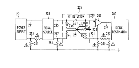
A DC coupled amplifier fed by an RF detector is disclosed which has
greater dynamic range capabilities than techniques in the prior art. An illustrative
embodiment of the present invention advantageously comprises a low-offset voltage,
low-offset current differential amplifier fed by an RF detector having a fifth lead
from the reference voltage node within the RF detector.


French Abstract

Amplificateur à couplage c.c. alimenté par un détecteur RF offrant une gamme dynamique plus étendue que celles qu'offrent les techniques existantes. Dans une application de la présente invention, un amplificateur différentiel à faible décalage et à faible courant est alimenté par un détecteur RF doté d'un cinquième conducteur relié au noeud de tension de référence du détecteur RF.

Claims

Note: Claims are shown in the official language in which they were submitted.


- 4 -
Claims:
1. An apparatus for detecting a signal, said
apparatus comprising:
an RF detector comprising:
(a) a signal-in lead,
(b) a ground-in lead,
(c) a signal-out lead,
(d) ground-reference lead, and
(e) a ground-out lead; and
a differential amplifier comprising:
(a) a first differential input connected to
said signal-out lead,
(b) a second differential input, of different
polarity than said first differential
input, connected to said ground-reference
lead,
(c) a ground lead connected to said ground-out
lead, and
(d) an amplifier output.

2. The apparatus of claim 1 wherein said
differential amplifier further comprises a composite
amplifier.

3. The apparatus of claim 2 wherein said composite
amplifier comprises:
(i) a low-speed, high-precision DC amplifier; and
(ii) a high-speed videoamplifier.

4. The apparatus of claim 3 wherein:
said low-speed, high-precision DC amplifier
comprises an output lead;
said high-speed videoamplifier comprises an
inverting lead and a non-inverting lead; and
said output lead is connected to said non-inverting
lead.

Description

Note: Descriptions are shown in the official language in which they were submitted.


21 24480


A DC COUPLED AMPLIFIER FED BY AN RF DETECTOR

Field of the Invention
The present invention relates to electric circuit
design in general, and more particularly, to methods and
apparatus which detect and amplify a DC coupled signal.

Backqround of the Invention
As shown in FIG. 1, RF detector 105 feed single-
ended amplifier 107 a DC coupled video signal. Depending
upon the mechanical construction of the apparatus
comprising RF detector 105 and single-ended amplifier
109, the return current from RF dector 105 can take
several paths. Bulkhead grounding through coaxial
connectors usually takes most of the current, but some
always flows through the sneak paths, represented by
ground resistors 151, causing a voltage error at the
reference ground lead 121. This voltage, while perhaps
only a millivolt, can easily drown the signal voltage in
applications that require a wide dynamic range. The
result is that part of the voltage error propagates
through RF detector 107 and is superimposed on top of the
signal on lead 125.

Summary of the Invention
The present invention provides a mechanism for
detecting a DC coupled RF signal while avoiding many of
the costs and restrictions associated with prior
techniques. Specifically, embodiments of the present
invention are generally less susceptible to ground loops
than techniques in the prior art.
These results are obtained in an illustrative
embodiment of the present invention which comprises an RF
detector and a differential amplifier wherein a first
differential input to the differential amplifier is
connected to the signal output of the RF detector and a
second differential input is connected to a reference
node in the RF detector.
, .

21 24480

- - la -

In accordance with one aspect of the present
invention there is provided an apparatus for detecting a
signal, said apparatus comprising: an RF detector
comprising: (a) a signal-in lead, (b) a ground-in lead,
(c) a signal-out lead, (d) ground-reference lead, and
(e) a ground-out lead; and a differential amplifier
comprising: (a) a first differential input connected to
said signal-out lead, (b) a second differential input, of
different polarity than said first differential input,
connected to said ground-reference lead, (c) a ground
lead connected to said ground-out lead, and (d) an
amplifier output.

Brief Description of the Drawinq
FIG. 1 shows a schematic diagram of a DC coupled
amplifier as in the prior art.
FIG. 2 shows a schematic diagram of an illustrative
embodiment of the present invention.

2124~80
-- 2 -
FIG. 3 shows an illustrative differential amplifier suitable for
incorporation in the illustrative embodiment shown in FIG. 2.

Detailed Description
FIG. 2 depicts a block diagram of an illustrative embodiment of the
5 present invention, which detects and amplifies a DC coupled RF signal. The
illustrative embodiment advantageously comprises: power supply 201, signal
source 203, RF detector 205, differential amplifier 207 and signal destination 209.
Signal source 203 is advantageously capable of amplitude modulating an RF signaland of outputting the modulated signal onto lead 215.
RF detector 205 advantageously comprises: diode 261, inductor 262,
capacitor 263, and reference node 231. Diode 261 is preferably a zero-based diode
or a tunnel diode between lead 215 and lead 219. Inductor 262 advantageously lies
between lead 215 and reference node 231. Capacitor 263 advantageously lies
between lead 219 and reference node 231. Resistors R 1,R2, and those designated by
15 151 are parasitic resistors caused by the mechanical connections, and by the bulk
resistivity of the metals. Typical values of resistance are in the range of 20 to 1000
micro-ohms.
Differential amplifier 207 is preferably a video amplifier (i.e., which
amplifies down to 0 Hz) and is characterized by a low offset voltage and a low offset
20 current. A schematic diagram of an illustrative differential amplifier suitable for
incorporation into the illustrative embodiment is shown in FIG. 3. The non-inverting
input of differential amplifier 207 is advantageously connected to the signal output
of RF detector 205 via lead 219. The inverting input of differential amplifier 207 is
advantageously connected to reference node 231 via lead 223. Since there is almost
25 no current in this lead, any resistance associated with the lead is of no consequence.
The non-inverting input of differential amplifier 207 can, however, alternately be
connected to reference node 231 when the inverting input is connected to the signal
output of RF detector 205. The output of differential amplifier 207 is fed into the
signal destination via lead 225. With this configuration, voltage offsets from the
30 parasitic resistances are canceled.
FIG. 3 shows a schematic diagram of a differential amplifier
characterized by a low offset voltage and a low offset current. This configuration is
often referred to as a composite amplifier. Differential amplifier 207 is a composite
amplifier comprising amplifier 301 and amplifier 303. Amplifier 301 is preferably a
35 low-speed, high-precision DC amplifier such as Analog Device's OP-227 and

2124~80


amplifier 303is preferably a high-speed, low-precision videoamplifier such as
Comlinear Corporation's CLC-401. The composite amplifier has the precision of
amplifier 301 and the speed of amplifier 303. Both amplifiers operate in conjunction
to force lead 309 to a virtual ground at all frequencies including DC. The inverting
S input 223 has much less bandwidth than the non-inverting input. From the abovedetailed description, it will be clear to those skilled in the art how to make and use
many variations of the present invention.

Representative Drawing
A single figure which represents the drawing illustrating the invention.
Administrative Status

For a clearer understanding of the status of the application/patent presented on this page, the site Disclaimer , as well as the definitions for Patent , Administrative Status , Maintenance Fee  and Payment History  should be consulted.

Administrative Status

Title Date
Forecasted Issue Date 1998-09-15
(22) Filed 1994-05-27
Examination Requested 1994-05-27
(41) Open to Public Inspection 1995-02-10
(45) Issued 1998-09-15
Deemed Expired 2003-05-27

Abandonment History

There is no abandonment history.

Payment History

Fee Type Anniversary Year Due Date Amount Paid Paid Date
Application Fee $0.00 1994-05-27
Registration of a document - section 124 $0.00 1994-11-18
Maintenance Fee - Application - New Act 2 1996-05-27 $100.00 1996-04-04
Maintenance Fee - Application - New Act 3 1997-05-27 $100.00 1997-04-07
Maintenance Fee - Application - New Act 4 1998-05-27 $100.00 1998-03-25
Final Fee $300.00 1998-05-11
Maintenance Fee - Patent - New Act 5 1999-05-27 $150.00 1999-03-19
Maintenance Fee - Patent - New Act 6 2000-05-29 $150.00 2000-03-20
Maintenance Fee - Patent - New Act 7 2001-05-28 $150.00 2001-03-19
Owners on Record

Note: Records showing the ownership history in alphabetical order.

Current Owners on Record
AMERICAN TELEPHONE AND TELEGRAPH COMPANY
Past Owners on Record
ARNTZ, BERNARD JAMES
Past Owners that do not appear in the "Owners on Record" listing will appear in other documentation within the application.
Documents

To view selected files, please enter reCAPTCHA code :


To view images, click a link in the Document Description column. To download the documents, select one or more checkboxes in the first column and then click the "Download Selected in PDF format (Zip Archive)" or the "Download Selected as Single PDF" button.

List of published and non-published patent-specific documents on the CPD .

If you have any difficulty accessing content, you can call the Client Service Centre at 1-866-997-1936 or send them an e-mail at CIPO Client Service Centre.


Document
Description 
Date
(yyyy-mm-dd) 
Number of pages   Size of Image (KB) 
Representative Drawing 1998-09-15 1 7
Cover Page 1995-08-26 1 63
Abstract 1995-08-26 1 30
Claims 1995-08-26 1 45
Drawings 1995-08-26 1 56
Description 1995-08-26 3 167
Cover Page 1998-09-15 1 35
Description 1997-10-22 4 138
Claims 1997-10-22 1 27
Drawings 1997-10-22 1 29
Correspondence 1998-05-11 1 38
Fees 1997-04-07 1 122
Fees 1996-04-04 1 46
Prosecution Correspondence 1994-05-27 6 241
Prosecution Correspondence 1997-09-17 2 58
Examiner Requisition 1997-03-18 2 65