Note: Descriptions are shown in the official language in which they were submitted.
CA 02124~44 1998-01-22
(a) TITLE OF THE lNv~NlION
METHOD AND APPARATUS OF MOUNTING A LENS
(b) TECHNICAL FIELD TO WHICH THE lNV~;N'l'ION RELATES
(c) BACKGROUND ART
This invention relates to a method and an apparatus for
mounting a lens on a semiconductor light emitting device which
is used as a light source in optoelectronic communications.
Laser diodes and light emitting diodes are typical
semiconductor light emitting devices. From the standpoint of
the material of the substrate, the semiconductor devices are
classified into a GaAs type, a GaP type, or an InP type.
These semiconductor devices emit light beams with different
wavelengths, because each material has different inherent band
gaps. The light emitting devices are also classified into two
types by the configuration of the emitted light beams. One is
a surface-emission type which emits light which is
perpendicular to a surface of films or a substrate. The other
is a side emission type which propagates light in a waveguide
which is parallel with a surface and emits light from a side
edge.
Optoelectronic communications or optoelectronic measure-
ments require small cores in fibres, because single-mode waves
are preferable for transmitting a signal for a long distance
without deformation or transmitting only one mode of signal.
Prior devices have adopting ball lenses for gathering beams
efficiently. A ball lens has shortness of focal distance and
isotropy. The short focal length effectively gathers light
beams. Geometric isotropy facilitates the mounting of a lens
on a semiconductor device. Ball lenses are directly fixed on
a light emitting device without space. The short focal length
forbids the ball lens from separating from the light emitting
device. A lens is thus fixed directly on a device. The
surface-emission type installs a ball lens directly on a chip
=~
CA 02124~44 1998-01-22
of a device without space or any spacer for gathering light
beams effectively. The mounting of a lens does not mean such
an indirect coupling of bonding a chip on a package and
encapsulating the package with a cylindrical cap having a lens
at a window. Such a package and a lens-cap may be employed to
seal the device at a later stage in order to fabricate double
lens devices.
Various ways have been proposed in order to fix a lens on
a light emitting device. A narrow core of an optical fibre
and a wide divergence of light beams emanating from an active
region demand a precise positioning of a lens. Small
deviations from the optimum spot greatly reduce the power of
the light entering the fibre core.
Japanese Patent Publication No. 57-29067 (29067/'82)
forms a circular cavity in a chip above the active (emanating)
region for positioning a lens. A semiconductor wafer is
provided lengthwise and crosswise with a plurality of units
comprising an emanating (active) region and a set of elec-
trodes. Cavities are formed either on the front surface or
the rear surface in correspondence to the positions of the
emanating regions. Then the wafer is cut lengthwise and
crosswise into a plurality of individual devices. The
separated devices are chips which contain a set of parts of a
semiconductor device. The chip is fitted to a suitable jig.
More recently, instead of the wafer processes, the
process begins with individual chips. Individual chips are
treated by the steps of filling an adhesive in the cavity,
supplying a ball lens into the cavity until the lens comes
into contact with the verge of the cavity, bringing the chip
into a furnace, and heating the adhesive to harden in order to
fix the lens. The adhesive is a material which is hardened by
heating. Since the cavities are dug by photolithography, the
cavities are exactly positioned with regard to the emanating
regions. Furthermore, since the ball lens is circumscribed
with the verge of the cavity, the lens is positioned to the
CA 02124~44 1998-01-22
cavity with high accuracy. If the light beams launch from the
epitaxial surface (front surface emission type), the relative
position of the cavity to the emanating region is rigorously
determined, because a series of photolithographic processes
are commonly applied to the same front surface.
However, in this method, it is important to position a
cavity with regard to the emanating region exactly for the
rear surface emission type device which emits light from the
substrate instead of from the epitaxial layer. Emanating
regions are made by selective doping of impurities from the
front surface of a wafer with the aid of photolithography.
Then the wafer is turned upside down. The cavities must be
formed in the rear surface by photolithography. Deformation,
bending or misorientation of the wafer induces errors in
positioning cavities themselves. Bilateral wafer processes
greatly injure the preciseness of positioning of the cavities
to the emanating regions.
Another drawback is the retention of adhesive in cavi-
ties. Since lenses are fitted in the cavities, after the
cavities are filled with the adhesive, some adhesive sometimes
remains above the verge of the cavities without being fully
excluded owing to the insufficient pressure of the lenses and
the strong viscosity. Then lenses float above the cavities
without being circumscribed. The floating of lenses on the
adhesive invites misalignments of lenses both in the vertical
direction and in the horizontal direction. The displacement
of the lens from the regular spot reduces the power of light
which converges on a core of a fibre which is positioned at a
predetermined place. Large deviations of the lens in the
horizontal directions will completely forbid the light
entering the fibre.
Japanese Patent Laying Open NO. 60-161684 aims to solve
the difficulty of the incomplete exclusion of adhesive out of
cavities. Instead of forming circular cavities, the improve-
ment forms sets of plural protrusions either on the front
CA 02124~44 1998-06-30
.
surface or on the rear surface of a wafer. The centre of the
set of the protrusions coincides with the centre of the
emanating region in the vertical direction. A set of protru-
sions are thus formed at the spots which are rotationally
symmetrical around a normal standing at the centre of the
emanating region. The method paints an adhesive on the
centres of the sets of protrusions, supplies ball lenses to
the centres of the protrusions, and fixes the lenses at the
centres by the adhesive. The lens contacts the protrusions at
the sides. The protrusions exactly position the ball lens at
a suitable spot. Extra adhesive will be excluded through the
wide gaps between the protrusions. Sufficient exclusion of
the adhesive seems to prohibit the ball lens from floating
above the surface. However, it has been found that the force
~5 of a lens to exclude an adhesive is in proportion to the
weight of the lens, because the lens presses the adhesive by
its gravity. Since the ball lens is small and light, the
gravity of the lens is so small that some extra adhesive still
remains at the centre of the protrusions. For example, a ball
~0 lens of a 300 ~ m diameter weighs only 0.00001 g (10 ~ g).
When the ball lens is placed on a fluid adhesive, the ball
lens slowly sinks in the adhesive. It takes a long time for
the lens to descend to the surface of the semiconductor.
Sometimes the adhesive hardens, before the lens attains the
surface. Then the lens is fixed at a point which is separated
from the surface. .
In both cases- of forming a cavity in, or forming
protrusions on, the front emission type enables the wafer
methods to harmonize the centre of the cavity or the set of
protrusions with the centre of the emanating region with
precision. However, the rear surface emission type includes
the wafer methods on both surfaces. At first, the emanating
regions are formed by epitaxy, impurity doping and
photolithography of the front surface. Then the wafer is
turned upside down. The cavities are produced in, or
CA 02124~44 1998-01-22
protrusions are produced on, the rear surface by
photolithography and etching. It is not easy to make the
centre of the cavities or protrusions coincide with the centre
of the emanating regions in the direction which is normal to
the surface. If the positioning is not correct, the centre of
the emanating region deviates from the centre of the cavity or
the set of protrusions. The ball lens gathers the light beams
emitted in various directions from the emanating region also
in the deviating case, but the lens does not converge the
beams on the core of a fibre. Almost all beams deviate from
the fibre. The deviation of the convergence prevents suffi-
cient power of beams from entering the fibre and weakens the
coupling between the light emitting device and the fibre.
This weak coupling is liable to induce malfunction due to the
insufficient power of light.
The names of surfaces will now be defined to avoid confu-
sion. Until now, the bottom of the substrate has been called
a rear surface and the top layer among epitaxially-grown
layers has been called a front surface. The front surface is
the surface nearer to the emanating region.
The selection of the emission surface depends on the
wavelength of the generated beams. The GaAs type device
having a GaAs substrate and AlGaAs epitaxial layers emits
light beams of a 0.85 ~ m wavelength. The GaAs of the sub-
strate absorbs the light of this wavelength. Thus the lightbeams cannot pass through the substrate, and the beams emerge
from the epitaxial layer surface. Therefore, the GaAs light
emitting devices belong to the front surface emission type.
The InP type device having an InP substrate and InGaAsP
epitaxial layers emits light of a wavelength of 1.3 ~ m. The
InP is transparent to the light of a 1.3 ~m wavelength. The
light beams can be taken out from the substrate. InGaAsP is
also transparent to the light of a 1.3 ~ m wavelength. The
light beams can go out from the epitaxial layers. Therefore,
the InP light emitting device can be fabricated into both the
CA 02124~44 1998-01-22
front surface emission type and the rear surface emission
type.
A light emitting device for optoelectronic communications
has a narrow emanating region. The optical fibre to be
connected to the device has a very narrow core. Single-mode
fibres have a core of a diameter of 5 ~ m to 7 ~ m. Graded-
index fibres have a core of a diameter of 50 ~ m to 62 ~ m.
Efficient coupling of a light emitting device to a lens
demands a rigorous positioning of a ball lens in the horizon-
tal directions. The deviation of the ball lens from theoptimum spot must be less than 5 ~ m in the horizontal
direction lX-, Y-directions). 5 ~ m is the maximum tolerance
of the position of ball lens.
However, the rear surface emission type device has an
emanating region on a surface and a converging lens on the
other surface of a chip. A series of wafer methods produces
emanating regions on the front surface. The other series of
wafer methods fabricates cavities or sets of protrusions on
the rear surface. The fabrication requires double wafer
methods, which invite a difficulty of positioning between both
surfaces besides the complexity of the wafer methods. The
problem of the positioning will be now explained.
Light emitting devices are fabricated on compound
semiconductor wafers, because light emission demands a direct
transition of electrons between a band gap. Silicon wafers
cannot be a substrate for light emitting devices, because
silicon forbids the direct transition of electrons. The
compound semiconductor wafer has an initial thickness of
400 ~ m to 500 ~ m. A series of wafer processes, i.e.,
epitaxial growth of films, selective etching, or formation of
electrodes produces a plurality of units of devices on the
compound semiconductor wafer. The unit of a device
corresponds to a part which will be an individual chip.
Epitaxial layers and electrodes are produced on a surface.
The surface having the epitaxial layers and electrodes is
CA 02124~44 1998-01-22
named a front surface, and the substrate bottom is named a
rear surface.
After the first wafer methods have fabricated units of
light emitting devices on the front surface, the rear surface
is ground in order to eliminate a part of the substrate. The
back grinding (gr;n~;ng of the rear surface) has three
purposes. One purpose is enhancing the thermal diffusivity by
th;nn;ng the wafer. In general, a large current flows at a
narrow active region in a light emitting device. The large
current density yields a great amount of heat at the active
region. The wafer must be made thinner in order to facilitate
the diffusion of heat.
Another purpose of the back gr;n~;ng is reducing the
absorption of light. The rear surface emission type will
lS incur much absorption loss of light, if the substrate is thick
and the distance between the emanating region and the rear
surface is long. Thus the rear surface must be ground in
order to reduce the absorption loss of light.
The most important purpose is adjusting the distance from
the ground surface (main surface to the emanating region at a
determined value. Dispersion of the distance will fluctuate
the convergence point, when a ball lens is glued to the main
surface. The third object of the back grinding is therefore
adjusting the distance between the ball lens and the emanating
region at a constant value.
The front surface bearing devices of the wafer is pasted
onto a polishing plate. The polishing plate is put on a
polishing turn table. The rear surface of the wafer touches
the turntable. The turntable revolves around a main shaft.
The polishing plate rotates around its axis. The rear surface
is ground until a predetermined thickness between 100 ~ m and
200 ~ m is obtained. The newly-revealed rear surface is
designated as a main surface. Then the thinned wafer is
removed from the polishing plate. Another series of wafer
methods form cavities in, or sets of protrusions on, the rear
CA 02124~44 1998-01-22
surface. In the methods, the centres of the emanating regions
on the front surface must coincide with the centres of the
cavities or the sets of protrusions on the rear surface.
However, it is difficult to harmonize the positions of parts
formed on the different surfaces. A series of wafer processes
ensures a high accuracy only for treating one surface. The
wafer processes on both surfaces impair the preciseness of
positioning of components because of the misalignment,
deformation or bending of wafer.
The semiconductor wafer for fabricating light emitting
devices is a large circular plate having a diameter of
2 inches to 3 inches. The individual chip of the light
emitting device is a small square of sides of 300 ~ m to 500
~ m. The devices are fabricated by the steps of forming a
plurality of emanating regions and electrodes lengthwise and
crosswise on the front surface of a wafer, grinding the rear
surface until a certain thickness is obtained, and forming
cavities in, or protrusions on, the rear surface by etching,
evaporation and photolithography.
The allowable error between the centre of the emanating
region and the centre of the cavity or the set of protrusions
must be less than + 5 ~ m. However, some bending accompanies
a processed wafer, because the wafer is wide but is very thin.
The error of positioning parts on both surfaces is further
increased by the size error of the masks for producing the
emanating regions or protrusions by lithography. The centres
of the emanating regions cannot easily coincide with the
centres of cavities or protrusions with a small error less
than the tolerance of + 5 ~ m.
Cavities are formed in, or sets of protrusions are formed
on, the rear surface. The wafer is divided into a plurality
of chips. A ball lens is fixed with an adhesive at the centre
of the cavity or the set of protrusions on the rear surface of
the individual chip. The adhesive is a type which hardens by
heating in a furnace. The method of mounting a lens is
CA 02124~44 1998-01-22
followed by the inspecting method. The inspection comprises
the steps of applying a current to the device for emitting
light beams, monitoring the light power, and eliminating
defective devices with light power which is smaller than a
determined value. The inspection is required partly because
the cavities in, or the protrusions on, the rear surface do
not always coincide with the emanating regions on the front
surface, and partly because the lenses sometimes deviate from
the regular spot by external vibration or shock before
hardening the adhesive in a furnace. After the lens-mounting
method has finished, the inspection begins in order to remove
malfunctioning devices. The difficulty of alignment on both
surfaces results in high rate of occurrence of defective
devices and in low yield of passing products. Furthermore,
since the cavity or the protrusions solely determine the
position of the lens by geometric anisotropy, there is no
means for revising the position of the lens at the mounting
method. The difficulty of alignment and the lack of the
position-revising means are likely to induce an occurrence of
malfunctioned devices in the whole wafer.
(d) DESCRIPTION OF THE lNvkNlION
This invention in its broad aspects aims at an improve-
ment of the surface-emission type of light emitting device.
Surface-emission type devices emanate light beams which are
perpendicular to an interface of layered films (pn junction).
Some emit light beams from a film surface, while others emit
light from a substrate surface. In order to distinguish two
types, the device emanating from the film surface is
temporarily called a "front surface emission type" and the
other device emitting from the substrate surface is now called
a "rear surface emission type". Light beams diverge in all
directions from a narrow active region without being guided by
a waveguide. Strong divergence of beams allows only a small
part of the beams to enter an end of an optical fibre. Thus
CA 02124~44 1998-01-22
-
most of the surface emission type devices employ a lens for
converging light beams in order to introduce the beams into a
core of a fibre.
A purpose of this invention is to provide a lens
mounting method and apparatus which enable a precise position-
ing of a lens on a chip which carries a lens directly on the
main surface in order to harmonize the centre of the emanating
region with the centre of the lens in the vertical direction.
An object of another aspect of the invention is to
provide a lens mounting method and apparatus which succeed in
eliminating the double wafer processes on both surfaces which
are apt to incur misalignment or discrepancy between both
surfaces.
An object of yet another aspect of the invention is to
provide a lens mounting method and apparatus which prevent
defective devices from occurring in the whole of a wafer by
quitting the double wafer processes.
An object of still another aspect of the invention is to
provide a lens mounting method and apparatus which fix a lens
in tight contact with a chip, and prohibit the lens from
deviating in the direction of a normal.
By one broad aspect of this invention, a method is
provided for mounting a lens on a light emitting diode chip
having a substrate, epitaxial layers grown on the substrate,
a pn-junction made in the epitaxial layers, a confined
emanating region formed by the pn-junction, a front surface of
the epitaxial layers and a main flat surface of the substrate,
and which is bonded with the front surface down on a package.
The method includes the steps of placing the package on an XY-
stage which can move in a horizontal XY-plane, replenishing a
driving current to the device chip, allowing the device to
emit light beams from the emanating region out of the main
surface. The emanating region is observed by a camera which
can displace in a vertical Z-direction, and the centre of the
emanating region is then determined by an intensity projection
,~
CA 02124~44 1998-01-22
method and a gravity measurement method. The centre of the
emanating region is harmonized with the centre of the camera
by moving the XY-stage in the XY-plane, and the XY-stage is
displaced by a predetermined distance in a predetermined
direction to a spot just below a dispenser which can move in
Z-direction. The dispenser is then lowered until a bottom tip
of the dispenser comes into contact with the device chip. A
dose of ultraviolet hardening resin is supplied to the chip
from the dispenser by contacting the dispenser with the chip;
lifting the dispenser up. The XY-stage is then displaced by
a predetermined distance in a predetermined direction to a
spot just beneath a vacuum collet holding a lens which can
move in the Z-direction. The vacuum collet is lowered until
the lens comes into contact with the resin and with the main
surface of the light emitting device chip, and the lens is
pushed against the chip by the vacuum collet. The ultraviolet
hardening resin is irradiated with ultraviolet rays to fix the
lens on the main surface of the chip by stiffening the resin.
The vacuum collet is then lifted from the lens.
By one variant of this aspect of the invention, the
dispenser moves downwardly in the Z-direction, the dispenser
falls quickly at an earlier stage and sinks slowly at a later
stage until it comes into contact with the device chip.
By another variant of this aspect of the invention, when
the vacuum collet having a lens displaces downwardly in the Z-
direction, the collet falls quickly at an early stage and
sinks slowly at a later stage until it comes into contact with
the chip.
By yet another variant of this aspect of the invention,
the dispenser supplies the main surface of the chip with an
amount of the ultraviolet hardening resin which is sufficient
to cover the sides of the diode chip, and the hardened
ultraviolet hardening resin on the sides protects the junction
of the device chip.
CA 02l24~44 l998-0l-22
- 12
By still another variant of this aspect of the invention,
the lens is transparent to the ultraviolet light irradiating
on the resin.
By a still further variant of this aspect of the
invention, two ultraviolet lamps are installed for irradiating
the ultraviolet rays on the resin which is painted on the chip
from different directions, the ultraviolet rays inclining at
20 degrees to 60 degrees to a horizontal plane, and the
projections of the rays on the horizontal plane make a
crossing angle of 90 degrees to 270 degrees. By a variation
of such variant, the ultraviolet har~le~;ng resin is 1.0 x 10⁻⁵
cc to 2.0 x 10⁻⁵ cc.
By a still further variant of this aspect of the
invention, the dispenser forms a resin ball at the bottom, the
diameter of the resin ball being 500 ~ m to 700 ~ m.
By yet a further variant of this aspect of the invention,
the whole vision of the camera is divided into a pixel matrix
consisting of columns and lines, the pixels are allocated with
intensity of light values, and the intensity projection method
sums the intensity of light values of all the pixels of all
lines and the intensity of light values of all the pixels of
all columns, and seeks the column and the line which give the
maximum sums as a rough estimation of the centre of emanation
region. By a variation thereof, a confined region is defined
with a determined size around the roughly sought centre, and
the gravity measurement method calculates the centre of
gravity in two dimensional space, and finds out a rigorous
coordinate of the centre of the emanation region.
By a still further variant of this aspect of the
invention, the tolerance of the error of the lens to the
centre is + 5 ~ m.
The present invention also provides an apparatus for
mounting a lens on a light emitting diode chip having a
substrate, epitaxial layers grown on the substrate, a pn-
junction made in the epitaxial layers, a confined emanating
CA 02124~44 1998-01-22
region formed by the pn-junction, a front surface of the
epitaxial layers and a main flat surface of the substrate, and
which is bonded with the front surface down on a package. The
apparatus includes: a device tray for laying a plurality of
light emitting device chips thereon; and a lens tray for
sustaining a plurality of lenses. An XY-stage is provided for
carrying the device tray and the lens tray in the X-direction
and in the Y-direction. A camera is provided for observing
the emanating region and for determining the centre of the
emanating region. A Z-stage is provided for displacing the
camera in the Z-direction. A dispenser is provided for
replenishing the device chip with an ultraviolet hardening
resin in contact with the chip, in which the Z-axis stage
supports the dispenser and for allows the dispenser to move up
and down. A mechanism is provided for moving the dispenser in
the Z-direction relatively to the Z-axis stage. A vacuum
collet is provided for holding a lens at a tip by air
pressure. A Z-axis stage is provided for moving a vacuum
collet in the Z-direction. A mechanism is provided for
permitting a relative motion to the Z-axis stage in Z-direc-
tion. Finally ultraviolet ray lamps are included for casting
ultraviolet rays to the resin on the device chip.
By one variant of this aspect of the invention, the Z-
axis stage of the dispenser is common with the Z-stage of the
vacuum collet.
By another variant of this aspect of the invention, the
Z-axis of the dispenser is independent of the Z-axis stage of
the vacuum collet.
By yet another variant of this aspect of the invention,
the vacuum collet has a cylindrical inner wall for holding a
lens.
By still another variant of this aspect of the invention,
the vacuum collet is provided with a trigonal pyramid inner
wall for holding a lens.
CA 02124~44 1998-01-22
- 14
By a still further variant of this aspect of the
invention, the dispenser is provided with a mechanism for
cancelling its weight; the dispenser is suspended by an
alleviated force by the Z-axis stage, the dispenser is adapted
to move upwardly in relation to the Z-axis stage when the
dispenser collides with the device chip, and an impulse acting
upon the device chip is reduced by the mechanism. By one
variation thereof, the cancelling mechanism comprises springs
which are adapted to raise the dispenser by an elastic force.
By another variation thereof, the cancelling mechanism
comprises balance weights which are adapted to raise the
dispenser by counterbalances.
By another variant of this aspect of the invention, the
vacuum collet is provided with a mechanism for alleviating the
weight, the collet is suspended by a reduced force by the Z-
axis stage when the vacuum collet touches the chip, the vacuum
collet is adapted to move upwardly relatively to the Z-axis
stage, and an impulse which is applied to the device chip is
decreased by the mechanism. By one variation thereof, the
cancelling mechanism comprises balance weights which are
adapted to raise the dispenser by counterbalances. By another
variation thereof, the cancelling mechanism comprises springs
which are adapted to lift the collet up by an elastic force.
As mentioned before, this invention in its broad aspects
aims at an improvement of the rear surface emission type
device. Furthermore, the lens mounting in the method of
aspects of this invention relates only to the direct coupling
of a lens to a chip.
The lens mounting method of one specific embodiment of
this invention includes the steps of grinding a rear surface
of a wafer having a front surface provided with a plurality of
light emitting devices including a emanating region and
electrodes lengthwise and crosswise. The thickness is
decreased until a predetermined value is achieved. The wafer
is divided into individual chips including an emanating
CA 02124~44 1998-01-22
region. The chip is fixed with the front surface down on a
stage. A driving current is supplied to an emanating region
of the chip in order to emit light from the rear surface and
the emanating region is observed by a TV camera. A centre of
the emanating region is determined by an intensity projection
method and a gravity measurement method. An ultraviolet
hardening resin is supplied on the centre. A lens which is
held by a vacuum collet is converged to the centre of the
emanating region. The lens is positioned at the centre in
contact with the rear surface. The ultraviolet har~en;ng
resin is irradiated with ultraviolet rays to harden the
ultraviolet hardening resin, and to fix the lens on the chip.
The vacuum collet is then detached from the lens.
Conventional methods depend upon the geometric anisotropy
lS of cavities or protrusions for positioning a lens without
seeking the centre of the actual emanating region. On the
contrary, this invention in its various aspects does not adopt
cavities, protrusions or other geometric anisotropy for
positioning of a lens. The centre of emanating region is
sought by optical methods. A lens is positioned at the sought
centre and is fixed there. Since the device is actually
ex~m;ned by supplying a current and measuring the light power,
no error occurs in positioning the lens.
Conventional methods lay a ball lens on an adhesive,
carry the chip in a furnace, heat the chip, and harden the
adhesive. External shocks or vibrations will induce the
deviation of a light lens, before the heat has hardened the
adhesive. Instead of heat-hardening adhesive, this invention
in its various aspects employs an ultraviolet hardening resin
so that the ball lens is fixed by means of an ultraviolet
hardening resin. The resin is hardened quickly by irradiation
with ultraviolet rays and it takes a short time to harden the
resin. The collet temporarily keeps the lens at the
determined spot until the resin fixes the ball lens.
.~
CA 02124~44 1998-01-22
- 16
The process of aspects of this invention will now be
explained in greater detail. The wafer with a rear surface
ground is divided into individual chips. The chip is laid
upside down on a stage which can move in two-dimensional,
horizontal space and has a positioning function with high
preciseness. A dispenser which ejects an adhesive can move in
the vertical direction (Z-direction) but does not move in the
horizontal directions (X-,Y-directions) . A vacuum collet
which suspends a lens can also displace only in the vertical
direction (Z-direction). The vacuum collet does not move in
the horizontal directions.
The power supply gives the device a driving current. The
sh; n; ng device is observed by a TV camera. The centre of the
emanating region is sought by an intensity projection method
and a gravity measurement method. Then the stage having a
chip is moved in the X- and the Y- directions until the centre
of the emanating region coincides with the centre of the TV
camera. The stage is moved by a determined distance in a
determined direction which is defined as the difference
between the TV camera and the dispenser. The centre of the
emanating region of the chip lies exactly beneath the tip of
the dispenser. The X-, Y-coordinates of the centre are equal
to the X-, Y-coordinates of the dispenser. Then the dispenser
falls in contact with the main (rear) surface of the chip and
ejects a definite amount of adhesive (an ultraviolet-hardening
resin) on the main surface. The dispenser rises and separates
from the chip. The stage moves in the XY-plane and attains a
spot just below the vacuum collet holding a ball lens. The
collet descends until the lens makes its way down in the resin
and comes into contact with the main surface. Ultraviolet
rays irradiate the adhesive resin, the resin then quickly
hardens.
The X-, Y-coordinates are predetermined for the TV
camera, the resin dispenser and the vacuum collet. The three
components cannot move in the X-direction or in the Y-direc-
CA 02124~44 1998-01-22
17
tion; but they can displace only in the Z-direction. (X1,
Y1), (X2, Y2) and (X3, Y3) denote two-dimensional coordinates
of the camera, the di~penser and the collet. The two-
dimensional difference between the camera and the dispenser is
designated by a vector C(Xc, Yc), where Xc = X2-X1, Yc = Y2-
Y1. The horizontal difference between the dispenser and the
collet is given by another vector D(Xd, Yd), where Xd = X3-X2,
Yd = Y3-Y2.
After the centre of the emanating region has been
adjusted to the centre of the camera, the stage carrying the
chip displaces by the vector C. so that the emanating region
lies exactly underneath the dispenser, and the dispenser
paints an adhesive on the main surface. The stage further
moves by the vector D. so that the emanating region exists
just beneath the collet. In short, by broad aspects of this
invention, this invention mounts a lens on a chip by the steps
of finding the centre of the emanating region by the camera,
displacing the chip by the feed C to a spot below the
dispenser, and displacing the chip by the other feed D to a
point underneath the collet. Since the feeds of C and D are
equal to the two-dimensional differences between two objects
of the camera, the dispenser and the collet, the exact
positioning by the camera enables the chip to displace just
below the dispenser or the collet. The positioning is exact
enough for the dispenser and the collet, because the camera,
dispenser and collet have no freedom of motion in the XY-
directions. Only the stage can move in the XY-plane.
The dispenser can rise and fall in the Z-direction so
that the dispenser directly contacts the chip and the tip of
the dispenser comes into contact with the rear surface. A
sensor monitors whether the tip is in contact with the chip.
If the contact is verified, the dispenser ejects a certain
amount of adhesive on the chip. The contact of the dispenser
ensures the precise supply of resin, because the contact
excludes the function of surface tension. The contact supply
CA 02124~44 1998-01-22
18
of resin is one of the features of aspects of this invention.
A shock absorber is furnished in order to alleviate the shock
of the collision and to avoid the breakage of a chip.
The vacuum collet carrying a lens is also lowered until
5the lens comes into contact with the chip. A sensor is
upholstered to monitor whether the lens is contacting to the
chip or not. A shock absorber is provided for alleviating the
shock of the collision. The collet presses the lens down
against the chip. Irrespective of the size of lens, all
10lenses become into contact to the surface, because the fall of
the lens is independent of gravity, and the lens never floats
on the adhesive. The contact exactly adjusts the distance
between the centre of the lens and the emanating region in the
Z-direction without ambiguity. While the lens is forced on
15the chip by the collet, the adhesive resin is hardened by
irradiating it with ultraviolet rays.
It is preferable that the dispenser and the collet should
move at two steps of speeds, i.e., a higher speed and a lower
speed, in order to attain a destination quickly and exactly.
20The converging lens is a ball lens or a spherical convex
lens. The vacuum collet has a tip for vacuuming a lens. The
inner contact wall of the tip is a cone or a trigonal pyramid.
A conical wall is easy to shape, but a trigonal wall precisely
maintains a lens at a spot, because the spot is uniquely
25defined as a point distanced from the three walls by the
radius of the lens.
The functions of aspects of this invention will now be
explained. The lens-mounting method of aspects of this
invention attaches a device chip on an XY-stage which is
30movable in both the X-direction and the Y-direction, supplies
a current to the light emitting diode chip for emitting light,
determines the centre of the emanating region by a television
camera, and harmonizes the centre of the emanating region with
the centre of the camera. Preferably, the recognition of the
35emanating region should be carried out by two steps. Firstly,
CA 02124~44 1998-01-22
19
an outline of the emanating region is roughly discovered in
the whole vision of the camera by an intensity projection
method. Secondly, the exact centre of the emanating region is
determined by a gravity measurement method in the confined
region enclosing the emanating region.
The two-step observation can shorten the time of
determ; n; ng the centre of the emanating region. The two-step
treatment can recognize the centre of the emanating region
with a reproducible preciseness less than + 0.1 ~ m in a
comparatively wide vision. Of course, the centre of the
emanating region can be determined with the same accuracy by
a single step in the gravity measurement method, but the
single step will take a longer time than the two-step
observation.
What conspicuously distinguishes aspects of this inven-
tion from the prior methods is determining the emanating
centre by supplying a current to the device, monitoring the
light by the camera and calculating the emanating centre.
Even if the positions of emanating regions fluctuate in
individual chips, the method of aspects of this invention can
mount lenses just above the centres of the emanating regions.
This invention in its various aspects is superior in the
preciseness of lens mounting to the prior method.
The formation of the cavities in, or protrusions on, a
surface needs an additional method in the prior art. This
invention in broad aspects dispenses with such an additional
method. Besides, the cavities or protrusions forbid free
positioning of a lens on a two-dimensional plane. The
geometric anisotropy destroys the freedom of positioning in
the plane.
This invention in its broad aspects does not form
cavities nor protrusions, but adopts a flat rear surface for
attaching a lens at an arbitrary spot. Geometric isotropy,
i.e., the flatness of the rear surface gives the two-dimen-
sional freedom of positioning to the chip. If the surface had
CA 02124~44 1998-01-22
_ 20
a cavity, the lens could not be placed at the optimum spot
which had been determined by the TV camera observation. The
formation of geometric anisotropy contradicts the free
positioning by the observation and pattern analysis. The flat
surface allows the method of aspects of this invention to fix
a lens at an arbitrary spot. The lack of cavities or protru-
sions has a positive significance in the method of aspects of
this invention. When the emanating centre is calculated, the
XY-stage is moved to harmonize the centre of the emanating
region of the chip with the centre of the vision of the
camera.
Now the emanating centre of the chip coincides with the
centre of the vision. Then the stage is shifted by a certain
distance to a certain direction which is denoted by vector C.
The chip lies just below the dispenser, because the feed of
vector C is equal to the two-dimensional difference between
the camera and the dispenser. The dispenser has a freedom of
movement in the Z-direction but has no freedom of movement in
the X-direction and the Y-direction. Since the camera does
not move in the XY-plane, the chip can be fed exactly
underneath the dispenser by shifting the stage by vector C.
Otherwise the lens mounting might be accomplished by the
simplified steps of harmonizing the emanating centre with the
camera centre, replenishing an adhesive from a slanting
dispenser to the chip, and supplying a lens from a slanting
collet to the adhesive. However, such a slanting way would
induce an anomalous distribution of resin and a deviation of
lens. The method of aspects of this invention allows the
dispenser to replenish resin vertically and the collet to
place a lens by a vertical motion.
Conventional methods have employed a heat-hardening
adhesive which is hardened by heating in a furnace, such
hardening requiring a long time. Accidental vibration
accompanies the conveyance to the furnace. The cavities or
CA 02124~44 1998-01-22
protrusions could stabilize the lens against the external
vibration.
Such a heat-hardening adhesive is inappropriate to the
method of aspects of this invention, because the vibration or
inclination of chips would induce a random shift of lens which
is simply laid on a flat surface without a cavity or protru-
sions.
The method of aspects of this invention requires an in-
site hardening adhesive which hardens quickly. This invention
thus adopts an ultraviolet hardening resin for fixing the
lens.
The dispenser which supplies a constant quantity of
adhesive to chips is equipped with a needle which ejects a
certain quantity of adhesive. In the dispenser, the adhesive
is compressed by air of a certain pressure for a certain time.
The adhesive goes out from the needle. The fluid adhesive
becomes a resin ball owing to the surface tension. The needle
falls until the tip comes into contact with the chip. The
resin is transferred to the chip in the contacting condition.
The contact supply excels quantitatively and the chip always
receives a determined quantity of resin. Prior methods
dropped an adhesive to a chip from an outlet which was
separated from the chip. The separated supply cannot suppress
the variations of the resin quantity due to the fluctuation of
the height of a chip or the fluctuation of the surface
tension. On the contrary, the contact supply allows the
method of aspects of this invention to suppress the fluctua-
tion of the quantity of resin in spite of the fluctuation of
the heights of chips.
Since the needle contacts chips, a protective device must
be contrived not to break chips. GaAs is mechanically weaker
than Si. InP is still more fragile for a shock than GaAs. In
general, a compound semiconductor is weaker than Si. Further
the chip is very thin. A little impulse easily breaks an InP
chip. Thus the dispenser should preferably be equipped with
CA 02124~44 1998-01-22
a mechanism for alleviating the weight of the dispenser. A
dose of the adhesive should be enough to flow on the sides and
cover the pn-junction of the chip. The resin will protect the
revealed pn-junction. Thus the adhesive resin plays a role of
a passivation film of guarding the junction in addition to
gluing the lens to the chip. The transfer of the resin from
the dispenser to the chip is called "transcriptionn.
When the resin has been transcribed, the dispenser is
lifted up. Then the XY-stage is shifted by vector D. The
feed of vector D is equal to the two-dimensional difference
between the dispenser and the collet. Thus, the chip lies
just underneath the vacuum collet which has vacuumed a lens at
the tip. The precision of positioning of a lens on a chip is
affected by the fluctuation of the position in the collet.
Preferably, the inner wall of the tip of the collet should be
shaped in accordance with the shape of the lens in order to
expel the ambiguity of positioning. For example, the tip of
a collet should be provided with a conical inner surface or
trigonal pyramid inner surface for a ball lens. The conical
surface is easy to shape because of the rotational symmetry.
The trigonal pyramid surface is rather difficult to cut, but
the trigonal pyramid ensures the exact holding of a lens owing
to the three point contact.
The vacuum collet also displaces only in the Z-direction.
When the chip has been conveyed beneath the collet, the collet
with a lens starts to fall. At first the collet descends
faster, but descends slowly afterward. For example, the first
speed of decent is 5 mm/s and the second speed of descent is
0.5 mm/s. The high speed decent of the first step shortens
the falling time. The slow decent of the later step lessens
the impulse of collision.
The method of aspects of this invention forces a lens to
come into contact with the main surface of a chip. The collet
presses the lens down to the surface instead of the use of
gravity upon which prior methods have relied. The contact of
CA 02124~44 1998-01-22
the lens to the chip uniquely determines the height of the
lens, which enhances the precision in the Z-direction and
curtails the time of mounting. On the other hand, the
compulsory contact of the lens would injure the chip. To
avoid the impairment, the collet should preferably be equipped
with the two step falling mechanism and a shock absorber.
The advantages of the method of aspects of this invention
will now be explained. The method of aspects of this inven-
tion mounts a lens on a chip of a light emitting diode which
emits light from the opposite (rear) surface to the emanating
region by the steps of supplying a current for emitting light,
observing the emanating region by a TV camera, calculating the
centre of the emanating region, harmonizing the emanating
centre with the centre of the camera, painting the centre of
the emanating region with ultraviolet hardening resin, putting
a lens on the resin, pushing down the lens to the chip, and
har~e~; ng the resin by irradiating the resin by ultraviolet
rays. Since the centre of the emanating region is sought for
individual chips by an actual observation, and a lens is fixed
on the real centre, the method of an aspect of this invention
succeeds in suppressing the error of positioning of lens
within the tolerance of + 5 ~ m.
No cavities are formed in the wafer nor protrusions are
formed on the wafer for the positioning of lens. The main
surfaces of chips are even. The flat surface can eliminate
the method of making the cavities or protrusions, which
simplifies the wafer processes. Besides, the exclusion of the
geometric anomaly guarantees the precise positioning of lens,
because the misalignment of lens has rather been caused by the
cavities or protrusions. The main surface is an even plane.
The even surface allows controlling the thickness of the wafer
exactly which has been polished. The flatness ensures an
accurate determination of the distance between the lens and
the emanating region.
CA 02124~44 1998-01-22
,
The contact transcription of the adhesive bestows the
dispenser with excellent quantitatively. The adhesive is
hardened quickly, while the collet holds the lens being in
contact with the chip, which exactly determines the distance
between the lens and the emanating region. The method of
aspects of this invention succeeds in the simplification of
wafer methods, the prevention of occurrence of defective
objects in the whole of a wafer, an enhancement of coupling
efficiency to a fibre, and a great reduction of cost of
production.
(e) DESCRIPTION OF THE FIGURES
In the accompanying drawings:
Fig. 1 is a perspective view of a lens-mounting apparatus
as an embodiment of this invention;
Fig. 2 is a plan view of the fields of vision of a camera
for explaining the principle of an intensity projection method
for roughly determining the centre of the emanating region;
Fig. 3 is a plan view of the confined region in the
fields of the camera for demonstrating a gravity measurement
method for determining the centre of the emanating region
rigorously;
Fig. 4 is a perspective view of a dispenser for ejecting
an adhesive on chips;
Fig. 5(a) and Fig. 5(b) are sectional views of a chip,
glue and a needle for explaining a conventional manner of
supplying glue (adhesive) to the chip, in which Fig. 5(a)
exhibits the state in which the needle ejects glue to the chip
separating from the needle, and Fig. 5(b) shows the state in
which the needle is lifted up;
Fig. 6(a), Fig. 6(b) and Fig. 6(c) are sectional views of
a chip, resin, and a needle for explaining the manner of this
invention for supplying resin to the chip, in which Fig. 6(a)
is a state in which a resin ball is formed, Fig. 6(b) is a
state in which a resin ball is formed, Fig. 6(b) is a state in
,,~
CA 02124~44 1998-01-22
,
which the needle is in contact with the chip, and Fig. 6(c) is
a state in which the needle is lifted away;
Fig. 7 is an oblique view of a holding apparatus of the
vacuum collet;
Fig. 8(1) and Fig. 8(2) are views of a conical collet, in
which Fig. 8(1) is a vertically-sectioned view and Fig. 8(2)
is a bottom view;
Fig. 9(1) and Fig. 9(2) are views of a sectional view of
a conical collet;
Fig. 10 is a sectional view of a collet, a lens and a
chip for demonstrating that the collet holds and pushes the
lens down to the chip;
Fig. 11 is a sectional view of a collet, a lens and a
chip for showing that the resin is hardened by the irradiation
of ultraviolet rays and the lens is kept by the collet;
Fig. 12 is a perspective view of the collet keeping the
lens against the chip and the resin irradiated by the ultravi-
olet rays from the irradiation heads; and
Fig. 13 is a sectional view of the light emitting device
(light emitting diode) having a lens above the emanating
region.
(f) ONE MODE FOR CARRYING OUT THE lNv~lION
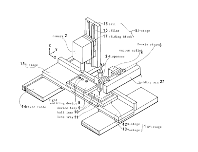
Fig. 1 shows an embodiment of a lens-mounting apparatus
of an aspect of this invention. The apparatus comprises an
XY-stage (1), a TV camera (2), a dispenser (3), a vacuum
collet (4), a camera Z-stage (5), and a collet Z-stage (6).
The XY-stage (1) conveys light emitting diode chips and lenses
in the horizontal place (XY-plane). Light emitting diode
chips (8) are laid on a device tray (9). Ball lenses (10) are
arranged on a lens tray (11). Both the device tray (9) and
the lens tray (11) are put on an X-stage (12). The X-stage
(12) rides on a Y-stage (13) which extends in the Y-direction.
The X-stage (12) can move in the Y-direction on the Y-stage
(13). The Y-stage (13) slidably lies on fixed tables (14)
CA 02124~44 1998-01-22
_ 26
which are long in the Y-direction. The Y-stage (13) can
freely move in the Y-direction on the table (14). The XY-
stage (1) consists of the X-stage (12) and the Y-stage (13).
In practice, the stages can be displaced at any positions
with high precision by motors, reduction gears or screw feeder
and bearings which allow the stages to move with little
friction. The embodiment employs an air-floating suspension
for holding the stages. Since the stages (12) and (13) are
floating on air over the Y-stage (13) and tables (14), the
stages (12) and (13) can displace without friction and can
pause at any points with preciseness. Resolution is 0.1 ~ m
both for the ~tages (12) and (13).
A plurality of light emitting diodes (8) are arranged
with the main (rear) surfaces upside lengthwise and crosswise
on the device tray (9). The light emitting diode chips have
been die-bonded on packages. Electrode pads of the chips are
connected to leads of the packages. If a current is applied
to the leads, the chips emit light beams from the main
surfaces.
A plurality of small holes have been formed lengthwise
and crosswise on the lens tray (11) and small ball lenses are
stored in the holes. Among the movable objects, only the XY-
stage (1) moves in the horizontal directions. The light
emitting devices (8) and the lenses (10) can displace in the
X-direction and the Y-direction. The camera (2), dispenser
(3) and vacuum collet (4) can displace only in the Z-
direction.
The infrared camera (2) can move in the vertical direc-
tion by the camera Z-stage (5). The Z-stage (5) comprises a
pillar (15), vertical rails (16) sliding blocks (17) which
slide up and down on the rails (16), a ball screw shaft (not
shown in the Figure) which is rotatably installed along the
rails (16), a ball nut which is fixed to the camera and which
engages with the feeding screw shaft, and a motor for rotating
the screw shaft. When the motor rotates the screw shaft, the
CA 02124~44 1998-01-22
ball nut is moved up or down, and the camera ascends or
descends with the ball nut. Since such a precise feeder is
well known, the details are not shown in the Figures. The
camera is equipped with a microscope in order to make an
S enlarged image of an object laid down below on a screen. The
focal point will be adjusted on the surface of the object by
the Z-stage (5) carrying the camera (2).
Firstly, the XY-stage (1) conveys a light emitting diode
chip (8) to a spot just underneath the camera (2). The camera
(2) determines the centre of the emanating region of the chip
by optical means and an image processing. The image
processing has two steps: Step 1: an intensity projection
method which seeks an outline of the emanating region in the
whole vision of camera; and Step 2: a gravity measurement
method which determines the exact centre of the emanating
region in a confined region.
The intensity projection method is explained by Fig. 1.
The whole vision of the camera is divided lengthwise and
crosswise like a lattice. The divided unit is called a pixel
which is a minimum component having a variable signifying the
degree of intensity of light entering the unit. The set of
pixels constructs a matrix. Two-dimensional coordinates are
attached to the pixels. The extreme left bottom is the
origin, and this pixel is numbered M~. J is the number of
lines. I is the number of columns. Thus i is the x-
coordinate and j is the y-coordinate in the unit of pixel.
(i.j) denotes an individual pixel defined in the two-
dimensional coordinate. M~ is a pixel lying at a spot of the
i-th in X-direction and the j-th in Y-direction.
For example, the size of the pixel is 1 ~ m x 1 ~ m in
the object space (real space). The camera has, for example,
500 x 500 pixels in the whole vision. In this case, the whole
vision of the camera corresponds to a square of 500 ~ m x 500
~ m (0.5 mm square) in the object plane. Firstly, a device
chip to be treated is carried within the vision of the camera
CA 02124~44 1998-01-22
by the XY-stage. A driving current is replenished to the
device from a power source through the leads and wires
equipped in the device tray. The device emits light beams
upward. The camera must have a sensitivity for the rays
emitted from the device. The camera thus would be changed
according to the wavelength of the light of the devices. If
the objects are InP light emitting diodes which cast infrared
light, the camera is an infrared camera which has high
sensitivity for infrared light. Otherwise, if the objects are
devices emitting visible light, the detector is an ordinary
camera.
The camera observes the rays which are emitted from the
emanating region. The image of the region is divided into
pixels. The intensity of light in an individual pixel is
classified into some degrees, for example, into 256 steps
(monochromatic degrees from white to black). "Mjj denotes the
light intensity of pixel Mjj. "n" is the number of pixels in
a line or in a column. The intensity projection method
calculates the X-sums of the intensities of the pixels
aligning in all columns, and the Y-sums of the intensities of
the pixels aligning in all lines. Here Xj denotes the
vertical sum of the intensities Mjj of the pixels Mjj belonging
to the i-th column. Yj designates the horizontal sum of the
intensities Mij of the pixels Mjj aligning in the j-th line.
Then the method finds out the column i and the line j which
maximize the sums among all the vertical sums and the horizon-
tal sums.
X; = ~ jl nmj (1)
Y~ nmij (2)
Xn~ = max{Xj} (3)
Xm~ = max{Yj} (4)
Line k=j denotes the line giving the maximum Yn~ among
the horizontal sums {Xj}. Column h=i denotes the column
realizing the maximum Xm~ among the vertical sums {Xj}.
Namely Yk=Yn~l Xh=Xn~. The result means that the centre of the
CA 02124~44 1998-01-22
29
emanating region must lie in the vicinity of pixel M~. The
emanating region should cast light beams in a regular distri-
bution which will maximize the sums of the intensities of the
column and of the line which cross the centre of the region.
This method projects the intensity on X-axis and Y-axis by
summing up the intensities of the pixels along the vertical
direction and horizontal direction. Thus it is called an
intensity projection method. Since this way includes only
addition, the calculation is quickly done. Besides the short
calculation time, this method has another merit. When the
vision includes reflection of external light or leak light
from the device itself, the gravity measurement in the whole
vision would misunderstand the centre of the emanating region.
Precedence of the intensity projection guarantees the avoid-
ance of the mistake in the recognition of the emanating
centre.
However, this method is not able to discover the pixel by
itself which actually maximizes the light power. The precise-
ness is contingent upon the size of a pixel. Rough recogni-
tion or outline detection is the purpose of the preceding
intensity projection method. If the distribution of the
intensity is steep enough, in the emanating region, it should
be preferable to thin out columns and lines into half or one
third in order to curtail the time of calculation.
The temporarily sought centre M~ of the emanating region
is displaced (see Fig. 3) to the centre of the camera. Then
the gravity measurement method is applied to the image of the
emanating region. Since the pattern of the emanating region
is restricted in the vicinity of the centre of the vision, the
object of consideration is confined in a small square which is
one tenth to four tenths of the whole vision. If the whole
vision is 500 ~ m x 500 ~ m, the confined region should be a
square of 50 ~ m x 50 ~ m to 200 ~ m x 200 ~ m. A narrower
square is also available for the confined region. The
confined region includes the centre of the emanating region.
CA 02124~44 1998-01-22
The number of pixels is far smaller than that of the whole
vision, which curtails the time of processing. The light
power mij of pixel Mij has been stored in a memory, for
example, in 256 steps. The centre of gravity G(Xg, Yg) is
calculated with a weight of intensity mij. Xi is the X-
coordinate of the i-th column. Yj is the y-coordinate of the
j-th line. The centre of gravity is determined by weight-
including averages of the coordinates.
i
~ i, jmii
yg= ~ i,jmijYj (6)
~i, j
The summation ~ is carried out with i and j of all the
pixels including in the confined region. The scope of the
average is not the whole vision but is the confined region
having a smaller number of pixels. Since a smaller number of
pixels are into consideration, the time of calculation is
curtailed.
The centre of gravity G(Xg, Yg) calculated now is
identified as the centre of the emanating region. The gravity
measurement method takes a longer time for calculation,
because it includes multiplication, and division besides
addition. The embodiment roughly estimates the centre of the
emanating region by the intensity projection method at first
and rigorously calculates the centre by the weight-including
gravity measurement method secondly.
Since the gravity measurement method includes the process
of averaging, the centre is determined with higher precision
than the unit of a pixel. Although the size of a pixel is
CA 02124~44 1998-01-22
1 ~ m x 1 ~ m, the coordinate of the centre can be defined
with the preciseness of 0.1 ~ m, which corresponds to the
resolution of the stages. A small displacement of the XY-
stage adjusts the centre of gravity with the centre of camera.
Now the centre of the emanating region coincides with the
centre of camera.
The relation between two-dimensional position (X1, Y1) of
the camera and two-dimensional position (X2, Y2) of the
dispenser is predetermined. Thus vector C (Xc, Yc) which has
been determined as a difference between the camera and the
dispenser is also predetermined. When the device has exactly
been positioned to the camera, the XY-stage is moved by vector
C. The emanating region of the chip comes to a spot just
below the dispenser.
The Z-axis stage (6) holds the dispenser (3), allowing it
to rise and descend. Fig. 4 shows the dispenser. The
dispenser (3) is a cylindrical vessel filled with ultraviolet
hardening resin. The resin is an adhesive which is hardened
by irradiation of ultraviolet rays instead of by heat or air.
The bottom end is formed into a narrow needle (20). The upper
opening is joined to a pipe (21) through which compressed air
is introduced to the upper space of the dispenser. A vertical
slide plate (22) holds the dispenser (3) by an upper retainer
(25) and a lower retainer (24). There is a linear guide (26)
at the back of the slide plate (22). The linear guide (26)
supports the vertical slide plate (22), allowing it to rise
and fall. The slide plate (22) is coupled to the linear guide
(26) by vertical rails and grooves (not shown in the figures).
The linear guide (26) is fixed to a Z-axis stage (6). The Z-
axis stage (6) is slidably supported by a rear holding arm(27). The linear guide (26) and the Z-axis stage can ascend
or descend with regard to the holding arm (27). A displace-
ment sensor (28) monitors the height of the slide plate (22).
The holding arm (27) is at rest. The Z-axis stage (6)
and the linear guide (26) move up and down in a body. The
CA 02l24~44 l998-06-30
-
32
slide plate (22) accompanies the Z-axi~ st3ge (6) and t~
linear guide (26) almost all the time. However, ~t~hen the
needle (20) comes into contact with the light emitting diqde
(8), the linear guide slightly slides on the linear guide
(26). At the moment the dispenser (3) stops but the linear
guide (26) and Z-stage (6) still continue falling. The
vertical rails and grooves allow the relative slide between
the slide plate (22) and the linear guide (26).
A stopper (29) projects forward from the Z-axis stage
0 (6). The slide plate (22) has an extension (30) on one side.
Almost all the time the extension (30) rides on the stopper
(29) of the Z-axis stage (6). The weight of the dispenser (3)
and the slide plate (22) transmits through the extension (30)
and the stopper (29) to the Z-axis stage (6). The coupling of
the stopper (29) and the extension (30) makes the slide plate
(22) accompany the linear guide (26) in almost all the motion.
The stopper (29) supports the extension (30) of the slide
plate (22) upwardly. The set of the stopper (29) and the
extension (30) allows the dispenser (3) to rise from the
linear guide a little but inhibits the dispenser (3) from
falling from the linear guide. The unilateral coupling of the
extension (30) and the stopper (29) alleviates the impulse
acting upon the chip (8) by separating the weight of the
linear guide (26) and the Z-axis stage (6) from the dispenser
(3), when the needle (20) collides with the chip (8). Besides
the unilateral coupling, the impulse on the chip is further
reduced by another mechanism.
The Z-axis stage (6) has a bracket (31) on the side. An
expa~ded spring (33) for counterbalance connects the bracket
(31) of the Z-axis with the extension (30) of the slide plate
(2~) by elastic force. Since the spring has been fitted
bet~oen the bracket (31) and the extension (30) in the
expanded sta'ce, this spring (33) gives the tensil~3 force to
the slide plate (22) for lifting up the dispenser (3). The
spring (33) reduces the impulse at the collision by pulling up
CA 02124~44 1998-01-22
the dispenser (3). There is an adjustment screw (32) at an
end of the spring for adjusting the tensile strength of the
spring (33).
Another spring (39) is furnished on the other side of the
S slide plate (22) to alleviate the shock of collision. The
slide plate (22) has a protuberance (34). The linear guide
(26) is provided with another protuberance (35). The spring
(36) is sandwiched in the compressed state between the
protuberances (34) and (35) for counterbalance. This com-
pressed spring (36) has a force for lifting the slide plate(22). The compressed spring (36) has the same function as the
extended spring (33). Both springs (33) and (36) play a role
of neutralizing the gravity of the dispenser (3) and slide
plate (22) and decreasing the impulse on chips (8).
W designates the weight of the dispenser (3) and the
slide plate (22). T denotes the tensile force of the extended
spring (33) for counterbalance. S denotes the compressive
force of the spring (36) for counterbalance. The resultant
force F acting between the stopper (29) and the extension (30)
is only F = W - T - S. This equation clearly demonstrates the
function of the springs (33) and (36) as counterbalances.
At the beginning stage of descent of the Z-axis stage
(6), the dispenser (3) and the slide plate (22) accompany the
Z-axis stage (6) and the linear guide (26). When the needle
(20) collides with the light emitting device chip (8), the
dispenser (3) and the slide plate (22) stop falling, but the
linear guide (26) and the Z-axis stage (6) continue
descending. At the moment, the movement of the linear guide
(26) and the Z-axis stage (6) is separated from the slide
plate (22). Since the linear guide (26) and the slide plate
(22) must fulfil different movements, the linear guide (26)
forgives the slide plate (22) for a relative rise. If the
relative movement were forbidden, the impulse would be so
strong and the device chip (8) would be broken.
CA 02124~44 1998-01-22
Since the device chip (8) is thin and fragile, the shock
at collision must be alleviated. Two contrivances contribute
to lessen the impulses. One is the two step descent of the Z-
axis stage (6): a faster descent at the earlier stage and a
slower descent at the latter stage. The slow contact
decreases the impulse of collision. The other is the
counterbalance due to the springs (33) and (36) which pull or
push upward the slide plate (22). The springs reduce the
force acting on the stopper (29) by the extension (30) from W
to W-T-S. This is equivalent to the effective decrease of the
mass of the dispenser and the slide plate to (W-T-S)/g, where
g is the gravity acceleration. The strength of the springs
should be adjusted in order to reduce the effective mass until
2 g to 5 g. Then the collision of the dispenser invites an
impulse not of an object with a mass W/g but of an object with
a mass of (W-T-S)/g. In this case, what strikes the chip is
a light object of a mass of 2 g to 5 g.
Another contrivance is the slow collision due to the two
step descent of the dispenser. When the needle of the
dispenser collides with the chip (8) at the speed v, the chip
incurs an impulse P of P=(W-T-S)v/g. The speed of descent v
is small enough to protect the chip by reducing the impulse.
The impulse equation P=(W-S-T)v/g clarifies the effects of the
two contrivances for alleviating the shock. The two-step
descending diminishes the speed v. The counterbalance springs
abate the effective weight of the dispenser by (-T-S).
Now the reason why the needle must come into contact with
the chip will be explained. First, the prior procedure is
demonstrated by Fig. 5, where the cavities or protrusions are
neglected here. The conventional method can be safely called
non-contact supply. The prior methods supply a glue in a
separated condition, for fear of breaking a chip. The needle
ejects a glue to the device chip (8) with a gap of t. The
fluid glue extends on the surface, as shown in Fig. 5(a). The
side of the glue has a random shape owing to the surface
CA 02l24~44 l998-0l-22
tension, and then the needle rises. Most of the resin
accompanies the needle (20) by the surface tension, as shown
in Fig. 5 (b). Since the chip is deprived of most of the glue
by the needle, the glue cannot cover the whole surface of the
chip, and the sides of the chip are uncovered, so that the
vulnerable pn-junction is exposed in air on the sides.
Another drawback would be induced by the shortage of painted
resin, if the prior supply would be applied to this invention.
As the prior method hardens the resin by heat, the shortage of
resin induces no difficulty. However, the method of aspects
of this invention adopts ultraviolet hardening resin which has
a special property. Insufficient resin is fatal to
ultraviolet hardening resin. If the amount of fluid resin is
insufficient, the resin is not hardened by the irradiation of
ultraviolet rays. The resin perhaps has a threshold regarding
the amount. Satisfactory ultraviolet rays cannot harden a
small amount of the resin which is less than the threshold
amount. Hardening is contingent upon the amount of resin.
The reason has not been clarified yet. Ultraviolet hardening
resin is anaerobic. The resin deteriorates rapidly in air.
Then a smaller drop of resin has a higher rate of surface /
volume, which heightens the chance of contacting oxygen for
resin molecules. A small drop of resin cannot prevent oxygen
from invading the drop to degenerate the property as an
adhesive. Such a reason may require a certain amount of resin
more than a threshold. The requirement is contingent on the
property of ultraviolet hardening resin.
Fig. 6 explains how to paint an ultraviolet hardening
resin on a chip in the method of an aspect of this invention.
Introduction of compressed air to the dispenser in a certain
time extrudes a dose of ultraviolet hardening resin from the
tip of the needle (20). Since the needle is still free, the
dose forms a ball of resin by the action of surface tension.
The ball is 500 ,'1 m to 700 11 m in diameter (0. 000012 CC to
0.000034 CC). The dispenser is lowered until the tip of the
CA 02l24~44 l998-0l-22
36
needle (20) comes into contact with the main surface of the
light emitting diode (8). The resin ball is transcribed to
the chip (8) in the contact state. The transcribed quantity
iS 1.0 X 10⁻⁵ CC to 2.0 x 10⁵ CC. A sufficient amount of
ultraviolet hardening resin pervades the main surface. Part
of the fluid drips on the sides. The fluid covers and
protects the pn-junction on the sides, as shown in Fig. 6(b).
The side-dripping resin has a role of a passivation film which
protects the device from oxygen, water or chemicals.
The transcription in the contact condition enables the
resin to transfer perfectly to the chip. The contact tran-
scription is superior in preciseness of dose and affluence of
supply to the prior separating transcription of Fig. 5. Since
a shortage of resin induces pool hardening due to oxygen, a
sufficient supply of resin is indispensable to the ultraviolet
hardening resin. The method of aspects of this invention
keeps the contact state for a certain time (e.g., 1 sec),
before the needle is lifted. The contact and the pause
guarantee a nearly complete transfer of resin to the chip.
Little resin remains on the needle (20) as shown in Fig. 6(c).
Then the XY-stage (1) is displaced by vector D(Xd, Yd).
Now the device chip (8) lies just underneath the vacuum collet
(4). Fig. 7 shows the vacuum collet (4). The vacuum collet
(4) is held by a vertically sliding plate (40). A linear
guide (41) suspends the sliding plate (40), allowing an upward
relative movement. The linear guide (41) is fixed to the Z-
axis stage (6). The Z-axis stage of the collet may be common
with the Z-axis stage of the dispenser (3), as shown in Fig.
1. Otherwise different z-axis stages are also available for
the dispenser and the collet, as shown in Fig. 4 and Fig. 7.
A displacement sensor (42) monitors the relative height
of the sliding plate (40) to the Z-axis stage (6). A pipe
(43) couples the vacuum collet (4) with a vacuum pump (not
shown in the figures). The linear guide is provided with a
stopper (44) projecting forward. The sliding plate (40) has
CA 02l24~44 l998-0l-22
a side protuberance (45). The protuberance (45) rides on the
stopper (44). Through the unilateral coupling, the linear
guide (41) supports the holding plate (40) upward.
The sliding plate (40) has a projection (46) on the front
surface. A lever (49) iS rotatably supported by a pin (48) on
the Z-axis stage (6). A front end (47) of the lever (49)
touches the lower side of the projection (46) of the sliding
plate (40). The lever (49) iS equipped with a balance weight
(50) at the other end. The balance weight (50) generates a
moment for holding up the sliding plate (40) and the collet
(4). The moment produced by the balance weight (50) can be
adjusted by the position of the weight. The vacuum collet (4)
pulls up a lens at the bottom tip.
G denotes the weight of the vacuum collet (4) and the
lens. R is the force of balance weight (50) for lifting the
sliding plate (40). The force H acting on the stopper (44)
and the projection (46) iS H = G - R. H shoul'd be adjusted to
several grams. H means the force pressing the lens toward the
chip. The balance weight (50) fills the role equivalent to
the springs (33) and (36) in Fig. 4. The balance weight (50)
reduces the effective force acting on the chip.
Like the dispenser, it is preferable for the vacuum
collet to descend faster at the early stage and slower at the
latter stage. The impulse upon the chip is (G-R)v/g at the
collision, where v is the descending speed of the collet.
Springs and balance weights are adopted for cancelling the
weight of the dispenser or the collet. Springs and weights
have a similar function for shock absorbers, but springs and
balance weights slightly differ from each other in decreasing
the shock. Springs have no inertia, and then springs can
cancel the weight from the moment of collision. Balance
weights have inertia. At the moment of collision, balance
weights cannot cancel the force of the dispenser or collet
owing to inertia. The balancers cancel the weight, after they
have attained to a stationary state. The delay time is the
''~..~
....
CA 02l24~44 l998-0l-22
38
square root of the quotient of rotation moment divided by
gravity accelerator g. However, in practice, the collet sinks
slowly. The slow descent of the collet enables the balancer
to absorb the impulse effectively. This example adopts
balance weights for the vacuum collet and springs for the
dispenser. Otherwise, the reverse selection is also
available. Springs can be adopted both for the collet and the
dispenser as a shock absorber. Balance weights can also be
employed both for the dispenser and the collet.
Holding a lens, the vacuum collet is prepared to supply
the lens to the chip. For this purpose, the vacuum collet has
been moved above a lens by displacing the XY-state (1), has
been lowered to the lens and has pulled up the lens. The
vacuum collet is waiting in the state.
Fig. 8 and Fig. 9 show examples of the tips of the vacuum
collet. Fig. 8 demonstrates a conical tip having a conical
inner surface. The tip has rotational symmetry. The simple
shape facilitates producing the collet. Fig. 9 shows a
trigonal pyramid collet having a trigonal pyramid inner wall.
Although the shaping is difficult, the trigonal surfaces
determine the position of a lens with precision due to three
point contacts.
Fig. 10 shows the state in which the vacuum collet (4)
pushes the lens (10) against the chip ( 8). The ball lens (10)
iS pressed to the main surface (51) of the chip by the collet
(4) which still holds the lens. The lens (10) lies just above
the emanating region (53). Part of the ultraviolet hardening
resin is excluded by the ball lens from the main surface. The
bottom of the lens is in contact with the main surface. No
resin remains between the main surface and the lens. Other
part of the resin encloses the sides of the chip. The pn-
junction is protected by the resin. The ultraviolet hardening
resin fulfils the role of a passivation film.
Fig. 11 shows the process of irradiation of ultraviolet
rays on the resin. Fig. 12 demonstrates the same process by
CA 02124~44 1998-01-22
a perspective view. While the collet keeps pushing the lens
against the chip, ultraviolet rays (55) are irradiated in
oblique directions to the ultraviolet hardening resin (52).
For example, light of a wavelength of 365 nm of a halogen lamp
is used for the ultraviolet rays for stiffening the resin.
The time of irradiation is 5 seconds to 10 seconds. The
oblique angle of the irradiation is 20 degrees to 60 degrees.
The existence of the collet gives the upper limit of the
inclination angle of the direction of ultraviolet rays. On
the contrary, too small an inclination angle invites a
shortage of irradiation to the resin and a defect of cohesion.
Further, it is preferable to install two ultraviolet ray
radiation heads (56) and (57) in order to irradiate the resin
from both directions. 90 degrees to 270 degrees is a prefera-
ble angle sandwiched by two imaginary lines which are producedby projecting the axes of the ultraviolet ray radiation heads
on the horizontal plane. The reason why two lamps are used
is the overall pervasion of ultraviolet rays on the resin.
Employment of two lamps is effective to avoid the occurrence
of dead angle for the rays. The lens casts a shadow on the
resin. Thus it is preferable to produce the lens by a
material which is transparent to the ultraviolet rays. If the
lens is opaque to the rays, the orientation of the lamps
should be adjusted to allot sufficient light to the resin
beneath the lens.
Fig. 13 is a section of the chip mounted with a lens. A
light emitting diode chip (8) is die-bonded with the front
surface down on the package (18). A lens (10) rides on the
main surface (51) of the chip (8). Ultraviolet ray hardening
resin (52) glues the lens (10) to the main surface of the chip
(8). The centre of the emanating region (53) coincides with
the centre of the lens in the vertical direction. Ultraviolet
ray hardening resin (52) also flows down to the sides of the
chip (8) and protects the junction (54). The ball lens is,
for example, 300 ~ m in diameter. The thickness of chip is
CA 02124~44 1998-01-22
_ 40
100 ~ m to 200 ~ m. The error in the horizontal direction is
less than + 5 ~ m which is the tolerance of position in the
example.
The lens-mounted chip is bonded on the package (18) which
is a disk with leads below. A cap with another bigger lens
(shot lens) is fitted to the package disc. The inner space is
airtightly sealed. This embodiment employs a ball lens.
However, the ball lens an be replaced by a cylindrical selfoc
lens or convex spherical lens. If another shape of lens is
adopted, the collet should have a different inner wall
suitable to handle the lens.