Note: Descriptions are shown in the official language in which they were submitted.
2 1 2 4 ~
~I~AT DI8~IPATING EMI/~FI PROTECTIVB
JUNCTION BOX AND CABI.E INTERFACB
The present invention is directed to the field of
structures for containing electrical and electronic
components and systems, and more particularly to enclosures
for circuit boards and connections thereof to electrical
conductor cables.
Card cages are known, in which a framework i8 provided
to define a card receiving region in which pairs of card
guides establish locations for insertion of daughter cards
therealong, for connectors mounted at a leading edge of each
thereof to mate with corresponding connectors of a backplane
traversing the rear of the card receiving region. The
backplane provides for electrical connections of the
circuits of each daughter card inserted to circuits of other
; daughter cards as desired or to conductors of input/output
cable. One such card cage is disclosed in U.S. Patent No.
~i 4,846,699 directed to a system for providing electrical
power to the components mounted on the daughter cards.
~ A backplane is disclosed in U. S. Patent No. 4,582,374
'`~! which interconnects a high density of signal circuits of
` cards mountable along a front face thereof with
corresponding circuits along a back face thereof, as well as
3 25 providing power interconnections and ground.
Another particular form of card cage is disclosed in
~; U.S. Patent No. 4,808,115 in which circuit cards mounted
` within modules are insertable into an enclosure or box
commonly referred to as a black box and containing a mother
board to which the circuit cards are interconnected. The
modules are referred to as line replaceable modules.
Aircraft have a great many electrical circuits
! interconnecting a variety of electrical articles thereon
' such as black boxes, sensors, instrument panels and the
j~'! 35 like, and the circuits are commonly interconnected in
: ! regions termed electronics bays. Various arrangements have
been devised to provide for disconnectable interconnections
. ~
'' 156~,~ CA .
.j .
-`` 2 1 2 ~
of the circuits and are known as wire integration systems.
Two such systems are disclosed in U. S. Patent No. 4,735,583
and 4,995,821. Discrete wire conductors are used to define
the interconnections.
The present invention provides an enclosure for an
array of individual circuit boards or daughter cards, a
backplane assembly to which the circuit boards are
electrically connectable and disconnectable, and an
input/output interface for electrically connecting the
backplane to cables of discrete electrical conductors, all
thus defining a junction box. The junction box includes a
front panel traversing the front face which is adapted to be
removable from the enclosure, a pair of opposing side walls,
upper and lower walls which include opposed pairs of card-
guiding channels extending rearwardly from the front face,
a backplane assembly traversing the rearward region of the
enclosure, and a rear wall which completes the enclosure and
provides for electrical connections of cables to the
backplane assembly. The junction box defines an integral
rugged electrically and thermally conductive envelope
surrounding the backplane assembly and daughter cards which
provides protection against electromagnetic interference
(EMI) and radiofrequency interference (RFI) to assure the
integrity of signals received, processed and transmitted by
the electronic circuîtry and components therewithin. The
junction box also provides heat dissipation for the
components therewithin which have been isolated from the
otherwise cooling effect of ambient air flow usually relied
upon to remove thermal energy from electronics bays.
The junction box is mountable to a shelf or other frame
structure as is conventional, in a manner similar to that
used for securing black boxes in electronics bays of
aircraft, and using a rack similar to conventional racks.
~i Used in association with the junction box is a rugged frame
j 35 mounted to the rack just rearwardly of the junction box on
¦ which are mounted connectors terminating the cables to be
156~ CA
2 1 2 ~
electrically connected to the backplane assembly within the
junction box. Mating faces of the cable connectors face
forwardly to mate with corresponding mating faces of cable-
associated connectors of the backplane assembly exposed
along the rear wall and facing rearwardly. During typical
mounting of the junction box into its in-service location,
the cables will already be installed in position within the
aircraft with the cable connectors secured to the rugged
frame mounted to the rack. The junction box is then
positioned on the rack and urged rearwardly to it6 installed
location, with the cable-associated connectors defined on
the rear wall mate with the cable connectors float-mounted
to the rugged frame, in a blind mating or rack-and-panel
arrangement. Preferably a large diameter pin extend~
forwardly from the frame to be received into a corresponding
hole of the rear wall of the junction box, cooperating to
enhance resistance to vibration and to wear. The junction
box is then secured in position by cooperation of locking
mechanisms secured to the rack with complementary lock
embossments on the bottom surface of the lower wall at the
front face. Electrically conductive gaskets surround every
opening in the junction box to provide an EMI/RFI seal at
each possible incremental gap during in-service use,
including the periphery of the front panel and the periphery
of the mating faces of the cable-associated connector along
the rear wall.
The front panel is securable to and removable from the
junction box in its installed condition, thus enabling
insertion and removal of individual daughter cards from the
junction box as desired and without requiring removal of the
~unction box from its installed position. Preferably the
front panel includes a pair of handles facilitating
manipulation thereof. With the front panel removed, each
daughter aard in a vertical orientation can be moved along
an associated pair of opposed guide channels extending
rearwardly from the front face to the forward face of the
15644 CA
2~2~
backplane assembly, and then clamped in the fully inserted
position all in a manner similar to conventional card cages.
The front panel includes an array of fins along the exterior
surface for dissipating thermal energy transmitted from the
interior during in-service use, by increasing the surface
area exposed to ambient air currents surrounding the
junction box. Along the interior surface of the front panel
is an array of fins at least including one associated with
the edge of each daughter card proximate the front face
after insertion, and preferably each interior fin includes
a ground clip mounted along the leading edge thereof to
become firmly engaged with the adjacent edge of the
associated daughter card to establish a ground connection
and a thermal connection with an electrically and thermally
conductive layer of the daughter card to establish an
enhanced heat-removal mechanism, as well as a means for
minimizing crosstalk between components of the various
daughter cards. Such ground clips mounted along the
interior fins are adapted to mate simultaneously with the
front edges of all the respective daughter cards in a blind
mate manner.
The backplane assembly includes a forward face
associated with the daughter cards, and a rearward face
associated with the cables. Preferably the rearward face is
defined by the rear wall of the junction box, and the
forward face is defined by a rugged interior panel member
mounted within the junction box. The forward face contains
an array of daughter card-associated electrical connectors
facing forwardly to be matable with complementary connectors
mounted on rear edges of the daughter cards, and
appropriately positioned with respect to the card-guiding
channels to become mated upon insertion of the daughter
cards, with the daughter card-associated connectors mounted
within apertures of the interior panel. Preferably the
card-associated connectors are mounted in a manner
permitting incremental adjustment in the plane of the panel
156~ CA
::
21 2~5a l
to precisely self-align the front contact sections of the
arrays of electrical contacts with contact sections of
corresponding arrays of complementary contacts of the card
edge connectors mounted on the daughter cards for remote
mating during daughter card insertion, enabling mating of
the individual pairs of mating contacts.
The rear contact sections of the electrical contacts of
the daughter card-associated connectors are electrically
connected to respective termini of circuit paths of a
circuit-bearing element which extend to opposed termini
electrically connected to rear contact sections of
corresponding electrical contacts of cable-associated
connectors mounted in the rear junction box wall. Front
contact sections of the corresponding contacts are exposed
for mating with complementary contact sections of the
contacts in the cable connectors secured in cutouts through
the rear frame. The backplane assembly thus electrically
interconnects respective circuits or wires of the cables
with appropriate circuits of the daughter cards.
The junction box of the present invention and the
backplane assembly also are especially useful to define a
wire integration system, in which circuits of the daughter
cards can be connected as desired to any particular
conductor of the input/output interface. A discrete member
such as a circuit card insertable into the card cage, is
disclosed which selectively interconnects the circuits
through the interconnection circuitry of the backplane
assembly. Such a discrete member, or matrix card, can be
programmed and reprogrammed easily, with no changes being
made which involve specific use customization or
modification to the backplane assembly, and which greatly
simplifies backplane construction for a high density of
thousands of individual circuits.
The rear wall includes integral shrouds surrounding the
mating faces of the cable-associated connectors which
interfit with complementary shrouds of the cable connectors
156~ CA
212~51
in a conventional plug/receptacle manner, and EMI/RFI ground
members are mounted peripherally around the plug ~hrouds to
establish a ground connection with the interior surface of
the receptacle shrouds thus grounding the cable shields to
the junction box and also assuring no EMI/RFI gap
surrounding the mating faces of the connectors in the mated
condition, and adapted to maintain such ground connection
during mechanical vibration during in-service use.
Preferably the cable connectors are mounted in apertures of
the rugged frame in a manner permitting incremental
transverse movement during mating upon initiation of the
interfitting of the plug shrouds with the receptacle shrouds
to precisely align the arrays of mating contact sections of
the mating connectors, all as the junction box is being
urged into its in-service position in the rack.
Backshells are easily mounted to the cable connectors
, and enclose the lengths of discrete conductor wires
i extending from each cable for EMI/RFI protection, and
include integral flanges to which the shielding braids of
each cable are affixed for grounding thereof; and the
backshells are adapted to be clamped to the cable outer
insulative jackets to provide strain relief for the cable
connectors. Each backshell may be an integral four-sided
member first placed loosely onto the cable prior to
terminating the conductors thereof to respective terminals
~ and securing the terminals into the housings of the cable; connectors, and then moved against the rugged metal shell of
the cable connector and mounted thereto before securing the
loaded connectors into respective apertures of the rugged
; 30 frame of the rack assembly, and then securing the shielding
braid about the backshell flange. In a second embodiment,
a backshell may also be assembled about the connector after
conductor termination and securing the connector to the
` frame, in which case the backshell may later be opened torepair or replace a terminal without first requiring total
\
1564~ CA
,
., .
~`
~,
2 1 2 4 5 ~
connector removal, and also permitting the drain wires to be
gro~nded to the backshell.
Preferably the circuit-bearing element is defined by an
array of overlaid layers of thin flexible circuit elements
or films permitting substantial latitude in the routing of
the discrete circuits. Such an arrangement permits the
termini connected to the card-associated connectors to be
defined in a plurality of first high density three-
dimensional arrays at a central region of the films adjacent
the rearward surface of the interior panel and associated
with respective ones of the card-associated connectors; the
circuits then extend laterally within the various layers of
flexible elements to intermediate regions laterally of the
first arrays to outer regions containing the second arrays
thereof; the intermediate regions enable the circuit-bearing
element to define gentle 180 bends for outer regions to be
doubled back to be parallel to and adjacent the rear wall
with the circuits concluding in termini defined in a
plurality of high density three-dimensional arrays
independent of the first arrays for electrical connection to
the contacts of the cable-associated connectors.
The backplane assembly can be fabricated as a
subassembly with the interior panel and rear wall mounted to
a plurality of posts about the peripheries thereof, with the
circuit-bearing element mounted therebetween already
electrically interconnecting the associated contact members
of the cable-associated connectors and card-associated
connectors. The plurality of posts preferably are guide
members insertable into and along opposed pairs of channels
defined at least along the interior surfaces of the upper
and lower walls of the junction box extending forwardly from
rear edges thereof, all positioned to align the card-
associated connectors with the appropriate card-guiding
channels. Fabrication of the backplane a~sembly can be
accomplished by mounting the card-associated connectors to
the interior panel, joining the rear contact sections of the
156~ CA
:
- , , . , , , - . - .
2124~1
contacts mounted in the dielectric housings thereof to
appropriate termini of the flexible film circuits and
joining the opposed termini to appropriate contact sections
of contacts of the cable-associated connectors, and then
securing the cable-associated connectors to the rear wall.
Preferably all of the film layers include pin-receiving
holes at all locations aligned with all electrical contacts
of all of the cable-associated and card-associated
connectors, with the circuit traces extending to termini for
the associated contact and isolated from all other pin-
receiving holes and with the traces except at the termini
being disposed between two layers of dielectric material, as
is conventional in flexible films.
One such process involves a layer-by-layer evolution by
placing the first or outermost film over the pin contact
sections of all of the connectors to extend through the
respective holes, and joining selected termini defined on
the first film layer to the appropriate contacts of the
cable-associated connectors and card-associated connectors;
placing the second film layer over the first layer with pin
contact sections through the holes and connecting its
termini to corresponding contacts; and continuing until all
layers are thus connected. Each film layer is adapted to
achieve the ultimate 1~0 bends to each side of the circuit-
bearing element by having incrementally different laterallengths of the intermediate regions of the films between the
first and second arrays, with the first or outermost layer
having the greatest lateral length and the last or innermost
layer having the least. As the layers are carefully built
up, the incremental difference in intermediate region
lengths results in inherent bends o~ the multilayer
structure to each side.
Alternatively, the layers may be initially stacked with
the hole arrays aligned at the card-associated region at the
center of the films, and the layers firmly adhered together
at the center such as by clamping and potting along the
: .
1564~ CA
2 1 2 4 ~
periphery; the holes are then plated in a process akin to
multi-layer printed circuit board fabrication, in which the
plating material extends along the aligned holes between the
two outermost layers, but with a conductive connection only
with the trace of the terminus of the particular layer with
which an electrical connection to a connector pin is
ultimately desired while plating material engages only
dielectric material of the other layers adjacent the
respective hole. Then upon insertion of pins through all
such plated holes and soldering of the pin end to the
plating material at the exposed outer layer, the pin is
conductively connected to the desired terminus. Connection
` of the cable-associated hole arrays can be performed
similarly with the plural layers formed about 180 and then
adhered at the ends after the hole arrays are aligned and
then plated and soldered, or as described in the first
process.
Preferably each daughter card rear edge includes
connectors mounted thereto to be disposed in large cavities
of an integral rugged conductive shell member mounted to the
daughter card rear edge. The integral shell includes a
card-mounting post by conventional mounting hardware at each
~`l end and a centrally located mounting post which is precisely
positioned with respect to the termini arrays of the
~ 25 circuits of the daughter card and thus defines a datum or
;~ reference for the electrical contacts contained in the
; dielectric housings of the daughter card connectors. This
~l arrangement assures that the contacts already assembled
'i within respective passageways of the housings prior to being
electrically connected to the respective termini, are
3 inherently precisely positioned by the housings within the
~' large cavities of the integral shell. This arrangement also
~,~ enables use of standard card-edge mountable connectors. The
integral shell further includes a forwardmost face which is
adapted to initially engage leading edges of the card-
associated connectors mounted in the interior panel of the
~` 156~ CA
.',
..
212~51
backplane assembly and incrementally laterally adjust the
position thereof to precisely align the contacts therein
with the associated contacts of the daughter card connectors
for blind mating. Also the integral shell may have key
members complementary with keys affixed to the interior
panel so that only the appropriate daughter card is
phy~ically able to be fully inserted into the selected card
location defined by the card-guiding channels for its
connectors to mate with the card-associated connectors.
Such integral shells also assist in minimizing crosstalk
between unrelated circuits and components within the
junction box, and are electrically and thermally connected
to the metal layer of each of the daughter cards, which are
electrically and thermally connected to the front panel of
the junction box for grounding and heat dissipation.
In addition to the array of daughter cards containing
electronic components mounted thereon including for example
microprocessors and integrated circuits, the junction box
includes a matrix card which is insertable into a particular
card location and includes arrays of pin contacts extending
from both surfaces thereof joined to discrete circuits
thereof. The pin contacts enable interconnection to others
thereof by jumper wires defining a circuit integration
system, and enahle customizing or programming the particular
junction box to serve a particular purpose in a manner
permitting and facilitating reprogramming later if desired.
Such a matrix card can include daughter card connectors
along the rear edge on both surfaces thereof for connection
of their contacts to circuits along both major surfaces
thereof. With no electronic components thereon and thus
minimal heat generation, no metal layer is needed on a major
surface of the matrix card for heat dissipation to the front
junction box panel.
It is an objective of the present invention to provide
a junction box adapted to enclose an electrical
interconnection of daughter card circuits to input\output
15644 CA
: :~
'.'~: :'`': ' : , ,, " ,': ' .' ' , . , " , . ' ....
2 ~ 2 4 ~
conductors, while providing protection of the ~ -
interconnections from electromagnetic and radiofrequency
energy to assure the integrity of the signals transmitted
across the interconnections.
It is also an objective for such a junction box to be
rugged, compact and light in weight.
It is an additional objective to provide such a
junction box which is adapted to dissipate thermal energy
from the interior of the junction box generated by the ~-~
daughter card components and the interconnections with
conductors contained therein.
It is a further objective to provide such a junction
box which enables access thereinto for removal and
replacement of a particular daughter card without requiring
removal of the junction box from its in-service position,
and without otherwise necessitating disconnecting any
remaining connections between other daughter cards and
associated input\output conductors, greatly minimizing down
time of an aircraft in which the junction box is mounted by
rendering moot the necessity for retesting of the circuits
and functions of the daughter cards not disconnected. ;~
An embodiment of the present invention will now be
disclosed by way of example with reference to the
accompanying drawings in which:
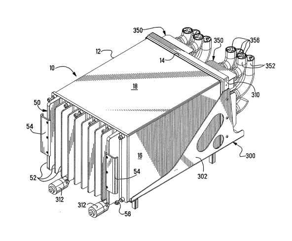
FIGURE 1 is an isometric view of the junction box of
the present invention secured in position within a rack
assembly;
FIGURE 2 is an exploded isometric view of the junction
box of FIG. 1;
FIGURES 3 and 4 are an isometric view of a spring clip
for establishing thermal junctions of daughter cards with
the junction box, and a plan view of a blank for the spring
clip;
FIGURES 5 and 6 are enlarged part section views of the
thermal junction of a daughter card and the junction box,
being assembled and fully defined, respectively; ~ ~ ~
~': ~: .:' :'
` 1564~ CA
','' ., . . : '. ' '
21~4`3~1
12
FIGURE 7 is an enlarged part section view of a fastener
for use in securing the front panel to the junction box of
FIGS. 1 and 2;
FIGURES 8 and 9 are isometric views of the rack
assembly of FIG. 1, assembled and exploded respectively,
showing the cable connectors mounted therein at the
input/output interface of the junction box and the rack
assembly;
FIGURE 10 is an isometric view of the rear wall of the
junction box, which is part of the backplane assembly for
the junction box, showing the input/output connectors
thereof at the input/output interface;
FIGURES 11 and 12 are part plan views and elevation
views in cross-section of the input/output interface between
the junction box and rack assembly of FIGS 1 to 10;
FIGURE 13 is an enlarged section view of a float mount
fastening arrangement of a cable connector in the frame of
the rack assembly of FIGS. 8 to 12;
FIGURE 14 is an isometric view of the backplane
assembly showing the daughter card interface thereof within
the junction box;
FIGURE 15 is a longitudinal section view illustrating
the mounting of the backplane assembly of FIGS. lO and 14
into the junction box of FIGS. 1 and 2 which contains a
daughter card positioned therewithin, and the front panel
- secured in place at the front face of the junction box;
FIGURES 16 to 18 are diagrammatic illustrations of a
method of constructing the backplane assembly of FIGS. 10,
14 and 15, showing discrete flexible circuit elements being
sequentially assembled to the connector terminal arrays, and
the forming of 180 bends in the elements resulting in the
interconnection circuitry of the backplane assembly, with
the rear wall being secured thereto in FIG. 18;
FIGURE 19 is an isometric view of a matrix card for use
with the backplane assembly of the junction box to integrate
. 156~ CA
. . .
-` 2~2~51 ~ ~:
13
the circuits, and showing a pair of integral shell members
containing the card-mounted connectors;
FIGURE 20 illustrates an integral shell of FIG. 19
being applied to a leading edge of the matrix card; and
FIGURES 21 and 22 are top and elevation views of the
integral shell of FIGS. 19 and 20 containing card connectors
therein, with terminal arrays for termination to circuits of
the card.
Junction box 10 of FIGS. 1 and 2 includes a box-like
body section 12, front panel 50 and rear wall 14 with body
section 12 having opposing side walls 16 and top wall 18 and
bottom wall 20 and extends from front face 22 to rear face
24 defining a card-receiviny region 26 extending inwardly
from front face 22. Front panel 50 includes an array of
exterior fins 52, to two of which are mounted a pair of
handles 54 enabling manual gripping of the front panel for
handling during removal from junction box 10, and is
mountable to front face 22 using fasteners 56 secured about
the periphery threaded into apertures of forward edges of
the top and bottom walls 18,20. Junction box 10 is
preferably used in conjunction with a rack assembly 300 such
as is shown in FIGS. 8 and 9 to which are secured cable~
terminated connectors 350, with junction box including a
backplane assembly 200 such as shown in FIGS. 10 and 14 for
interconnecting the cable's conductors with circuits of an
array of daughter cards 100 in the junction box.
In FIG. 1 junction box 10 is shown in position mounted
within tray section 302 of rack assembly 300 for in-service
use, with rack assembly 300 mounted on a shelf (not shown)
within a structure such as an aircraft or ship. Junction
box 10 is slidable along a box-receiving path 304 defined by
bottom wall 306 and side walls 308, and is shown abutting
panel member 310 traversing the end of box-receiving path
304. Panel member 310 is a rugged frame firmly affixed to
tray section 302, and includes mounted thereto several
electrical connectors 350 terminating a plurality of cables
156~ CA
2 1 2~
352 containing multiple electrical conductors 354. Junction
box 10 is locked in position using locking hardware 312 at
the forward end of tray section 302, engaging locking
embossments 28 depending from junction box 10 proximate
front face 22.
Junction box 10 is shown in greater detail in FIG. 2,
with card-receiving region 26 including opposing pairs of
card guide channels 30 extending inwardly from front face 22
to define guides for insertion of circuit cards such as
daughter card 100 and matrix card 130. Thus junction box is
) essentially a compact, fully enclosed card cage. Backplane', assembly 200 is provided proximate rear face 24 and includes
a forward wall section 202 traversing the inwardmost extent
of card-receiving region 26. Mounted onto forward wall
section 202 is an array of card-associated electrical
connectors 204 matable with complementary connectors 102
affixed to leading edges 104,134 of daughter cards 100 and
matrix card 130. Backplane assembly 200 further includes
interconnection circuitry 206 extending from forward wall
section 202 to rearward wall section 14, which may comprise
the rear wall of junction box 10 as shown if desired. Rear
wall 14 includes mounted thereon an array of electrical
input/output connectors 208 corresponding to connectors 350
mounted on frame member 310 of rack assembly 300.
Preferably rear wall 14 is joined to forward wall section
202 by a plurality of struts 216 peripherally of
interconnection circuitry 206, so that backplane assembly
~; 200 is manipulatable as a unit or subassembly insertable
i into body section 12 of junction box 10 at rear face 24
whereafter rear wall 14 is fastenable to rear edges of side
walls 16 and top and bottom walls 18,20 thereof.
Junction box 10 defines an integral rugged electrically
, conductive envelope surrounding the backplane assembly and
` daughter cards which provides protection against
electromagnetic and radiofrequency interference to assure
~ the integrity of signals received, processed and transmitted
.~ 156~ ~A
2124~1
by the electronic circuitry and components therewithin. The
junction box also provides heat dissipation for the
components and interconnections therewithin which have
become isolated from the otherwise cooling effect of ambient
air flow usually relied upon to remove thermal energy from
electronics bays. Side walls 16, top and bottom walls
18,20, rear wall 14 and front panel 50 are preferably formed
of an electrically conductive alloy with superior thermal
conductivity such as aluminum Alloy No. 6061 suitable for
welding. Further preferably, all seams between the wall
members of the junction box are tight fitting such as by
being welded or even extruded integrally, or with resilient
conductive EMI gaskets used where necessary such as the
mounting interface of the front panel with the front face,
and at the openings or cutouts 228 in rear wall 14 for
input/output connectors 208 (gaskets 229 of FIG.17), thus
eliminating all gaps which otherwise could permit EMI/RFI
leakage into and out of the junction box. Such gaskets
could be of conductive elastomer sold as CH0-SEAL 1285 by
Chromerics, Inc.
The junction box thus provides a compact card cage of
robust construction adapted to shield circuit cards and
interconnections of circuits thereof with input/output
conductors. With use of matrix card 130 or similar element
the junction box has a circuit integration capability
enabling simplification of the backplane assembly to become
compact for a high population of circuit interconnections.
Embossments 28 are seen depending from bottom wall 20
at the front edge thereof, and are designed to be engaged by
locking hardware 312 of rack assembly 300 when junction box
10 is inserted fully into rack assembly 300. By being
affixed to bottom wall 20, locking hardware 312 and
embossments 28 continue holding junction box 10 in its
locked in-service position mated to panel member 310 of rack
assembly 300 at the input/output interface even when front
panel 50 is removed from front face 22; the arrangement
564~ CA
212~
16
permits opening the junction box ~or insertion or removal of
a particular daughter card while permitting all other
daughter cards to remain in position with their circuits
fully connected through the backplane assembly to the
input/output conductors at the input/output interface at
rear wall 14 and panel member 310 of rack assembly 300.
Such capability greatly minimizes down time of an aircraft
in which the junction box is mounted by rendering moot the
necessity for retesting of the circuits and functions of the
daughter cards not disconnected. Locking hardware may be of
the extractor holddown type disclosed in U.S. Patent No.
3,640,141.
Further seen in FIG. 2, front panel 50 includes an
array of interior fins 58 associated with respective
daughter cards 100 and extending to card~proximate ends 60
on which are mounted spring clips 62. Spring clips 62 are
adapted to capture trailing ends 106 of all daughter cards
simultaneously upon mounting of front panel 50 in place
across front face 22 in a manner permitting simultaneous
disengagement, to engage trailing end 106 at pluralities of
locations to establish thermal junctions 64 therewith (FIG.
6). Thermal junctions transfer heat from the daughter cards
to the interior fins, and front panel 50 dissipates the heat
from the daughter cards and interior of the junction box,
especially through exterior fins 52. Rear wall 14 also is
shown to have interior fins 58 which likewise provide heat
dissipation benefits.
In FIG. 3 is shown a spring clip 62 mountable to card-
proximate ends 60 of interior fins 58 of front panel 50 of
junction box 10, with spring clip 62 formed from a blanh 62A
as shown in FIG. 4, and with FIGS. 5 and 6 illustrating
spring clip 62 mounted to a fin and establishing a thermal
junction 64 with a daughter card trailing edge 106. Spring
clip 62 is disclosed in greater detail in U.S. Patent
Application Serial No. 08/076,614 filed June 11, 1993.
1564~ CA
212~
~7
Suc~ spring clips mounted along the interior fins are
adapted to mate simultaneously with the front edges of all
the respective daughter cards in a blind mate manner.
Preferably spring clips 62 are formed of metal stock such as
5beryllium copper Alloy No. 25, full hard temper and be
sufficiently thick to possess strong spring properties such
as 0.010 inches thick.
Each spring clip 62 includes a mounting section 66,
body section 68 extending therefrom, and an array of spring
10arms 70 extending from body section 68 to respective free
ends 72. Preferably mounting section 66 is adapted to be
joined to a card-remote portion of a respective fin 58, such
as surface 74 facinq away from the associated circuit card
trailing edge 106. Mounting section 66 can comprise an
15array of spring arms ~6 extending from bight sections 78
joined to body section 68 around fin end 60 and along card-
remote surface 74 to free ends 80. Each free end 80
comprises a short section extending perpendicularly to card~
remote surface 74 of fin 58 to be received into recess 82
20thereof defining a locking surface 84. Mounting spring arms
76 are so formed at bight sections 78 and have free ends 80
extending to an edge 86 so positioned a short distance from
body section 68 in the unstressed state compared to the
thickness of interior fin 58 at recess 82, that free ends 80
25are held therein by strong clamping spring bias able to
resist being pulled off card-proximate fin ends 60 during
front panel removal.
Body section 68 is integral and elongate to extend
along most of trailing edge 106 of a daughter card 100, and
30extends from mounting section 66 and along a card-proximate
surface 88 of fin 58 to be parallel and adjacent to a
trailing edge portion 106 of daughter card 100. A spring
arm section is adjoined to body section 68, such as an array
of discrete spring arms 70 joined at respective bight
35sections 90 positioned forwardly of trailing edge 106 upon
full assembly of the circuit card in the junction box and -
156~ CA
,
-
2124~
placement of front panel 50 along front face 22. Each
spring arm 70 extends to a constriction 92 and concludes at
a free end section 94 diverging from body section 68 at
card-proximate fin end 60 and defining an edge-receiving
entrance. Constriction 92 is dimensioned less than the
thickness of a daughter card 100, and upon entry of the
trailing card edge thereinto spring arms 70 are deflected
outwardly and thereafter assuredly urge trailing edge
portions 106 inwardly against body section 68 of a
respective spring clip 62 at a plurality of locations along
trailing edge 106 establishing an array of thermal junctions
therewith.
Each elongate spring clip 62 with opposed arrays of
spring arms 70,76 of such serpentine cross-section can be
made using a blank 62A as shown in FIG. 4, by using for
example a plurality of sets of elongate dies in a press
apparatus (not shown) in a progression of forming steps and
preferably a progression of such steps for particular ones
of the bight sections to consistently and carefully attain
the desired bight radii and resultant dimensions at
constrictions 92 and mounting free ends 80 in the unstressed
state.
When used with daughter cards 100 having a metal layer
110 for optimized thermal conductivity to the card's edge,
the spring clips are preferably electrically conductive and
serve to establish an assured ground of the metal layers to
the conductive enclosure, facilitating the performance of
the metal layers in minimizing crosstalk between the
components of the various cards.
FIG. 7 is an enlarged section view of a fastener
assembly 56 of the type especially useful in mounting front
panel 50 to front face 22 of junction box 10. Such fastener
assembly 56 is conventional and one example is a captive
panel screw available from Amatom, Inc. under Part Nos.
6766-SS-0832 and 6254B-SS-1032. Housing 160 includes an
axially extending flange 162 pressfit into a large-diameter
15644 CA
``` 2124:~51
19
aperture 164 into front panel 50. Tool-engageable head 166
of screw member 168 is exposed outwardly of housing 160;
elongate small diameter shank 170 extends through cavity 172
of housing 160 to large diameter threaded end portion 174
threadable into correspondingly threaded aperture 176 in
forward edges of top and bottom walls 18,20 of body section
12 of junction box 10. Upon screw member 168 being rotated
to unthread end portion 174 from aperture 176, larger-
diameter threaded end portion 174 is received into housing
cavity 172 which maintains it captive in the fully
unthreaded state. With such fasteners, no loose parts exist
needing to be specially handled especially during
rethreading, or possibly to become misplaced during the
process of removing and replacing front panel 50 from front
face 22 of junction box 10.
Rack assembly 300 is shown in FIGS. 8 and 9, and is of
the type disclosed in U.S. Patent Application Serial No.
08/076,655, filed June 11, 1993. Bottom wall 306 and side
walls 308 define a box-receiving path 304 extending to frame
member 310, so that cable connectors 350 mounted thereon are
positioned to become mated with corresponding input/output
connectors 208 of the rear wall of the junction box when
junction box 10 is fully installed by being moved along box-
receiving path 304. The arrangement per~its all cables 352
to be installed as complete cable harnesses into an aircraft
(along with rack assembly) separate in time from
installation of the junction box, and permitting automatic
mating of the connectors merely upon junction box being
installed.
Rear wall 14 of junction box 10 shown in FIG. 10, which
is shown to be a portion of backplane assembly 200, to
contain an array of input/output connectors 20B mounted
therealong, simultaneously matable with cable connectors 350
on frame member 310, as illustrated in FIGS. 11 and 12.
Cable connectors 350 include dielectric housings 354
containing discrete terminals terminated to conductors 356
15644 CA
: :
,. . .
2 1 2 ~
of the cables with contact sections 358 exposed at mating
faces thereof. Dielectric housings 354 are secured within
cavities 360 of multiconnector sh~ll members 362, and
backshells 364 are affixed to rearward faces 366 of the
shell members 362 to enclose lengths of discrete conductor
wires 356 extending from each cable 352 for EMI/RFI
protection, and include integral flanges 368 to which the
shielding braids~370 of each cable 352 are affixed for
grounding thereof; and the backshells 364 may be clamped to
the cable outer insulative jackets 372 to provide strain
relief for the cable connectors 350, if desired. A
representative resilient conductive EMI gasket 374 is shown
disposed between backshells 364 and shell members 362
peripherally about the cavities and along the mounting
interface eliminating any gap which otherwise could permit
EMI/RFI leakage therethrough to eventually pass along the
conductors and into the junction box. Also, connectors 350
are shown to include a means for terminating drain wires of
cables 352, such as an embossment 390 of shell 362 in FIG.
12 to which a drain wire 392 is connected by a screw 394, or
an embossment 390A on the back wall of a backshell 364A by
a screw 394 in FIG. 12.
Each shell member 362 is mountable within a cutout 314
of the panel member 310 or frame, using fasteners 316 which
extend through recesses 318 about the cutout 314 and through
apertures through mounting ears 376 of shell member 362.
Mounting ears 374 are received into corresponding recesses
320 along cable face 322 of frame 310, and heads 324 of
fasteners 316 are received into recesses 326 permitting the
fastener heads to be disposed below the forward surface 328
of frame 310, clear of interfering with abutting engagement
of frame 310 and junction box rear wall 14.
With reference especially to FIG. 13, shell members 362
each include a peripheral flange extending through the
corresponding cutout 314 and are dimensioned slightly
smaller than the cutout; the mounting ears 376 are also
1564~ CA
~' '''~:
... . .... . .. . ..
- 2 1 2 4 ~
21
slightly smaller than the recesses 320 of frame 310 into
which they are received; and shanks 330 of fasteners 316 are
slightly smaller than recesses 326 of the frame through
which they extend. This arrangement permits the shell
members to float within cutouts 314 of frame 310, enabling
incremental transverse adjustment of the cable connectors
350 during blind mating with corresponding connectors along
rear wall 14 of junction box 10 in order to precisely align
the contact sections 358 of the terminals of the cable
connectors with opposed contact sections 210 of mating
terminals of the connectors of the junction box. Initial
engagement to incur the adjustment is established by leading
edges of shrouds 378 surrounding mating faces of respective
housings 354 which are received as plug sections into
lS receptacle sections 212 of shells 214 surrounding mating
faces of mating connectors 208. Circumferential EMI spring
strips 380 will establish an assured ground connection
between shrouds 378 and receptacle sections 212 upon mating;
an O-ring 382 is shown about each shroud 378 also to assist
in sealing the interface i~ desired.
Also seen in FIGS. 8 to 10 is post member 384 affixed
to frame 310 and extending forwardly into the input/output
interface to be received into a complementary post-receiving
hole 386 into rear wall 14 of junction box 10 upon
installation of junction box 10 in rack assembly 300. Post
member 384 within hole 386 serves to maintain the position
of junction box 10 within rack assembly 300 after
installation to absorb stresses resulting from vibration of
an aircraft which otherwise could stress the mated
connectors and their mated terminals during in-service use
and possibly even lead to intolerable momentary signal
discontinuity; the post member also provides wear resistance
benefits.
Backplane assembly 200 for junction box 10 is
illustrated more clearly in FIGS. lO and 14 and is disclo~ed
in U.S. Patent Application Serial No. 08/076,656 filed June
1564~ CA
,., ~ ., , . ' - ' ' ' ' . ' ', , . . ~ . '' ~
.:., ~ ' . .. , ., -. ' .'' ' ' ' ,' , . ',
2 1 2 4 ~
22
11, 1993. Strut members 216 extend between upper and lower
edges of rearward wall section 14 and bosses 218 along upper
and lower edges of forward wall section 202, thus securing
forward and rearward wall sections 202,14 together.
Interconnection circuitry 206 is disposed therebetween. A
first connection region is defined which provides
connections between circuits of the interconnection
circuitry with terminals 220 of card-associated connectors
204 mounted in forward wall section 202, which mate with
corresponding terminals of connectors 102 mounted on leading
edges 104 of daughter cards 100 and matrix card 130 (see
FIGS. 2 and 19). A second connection region is defined
along rearward wall section 14 which provides connections
between circuits with terminals 210 of input/output
connectors 208 mounted in rearward wall section 14, which
mate with corresponding terminals of cable connectors 350
mounted on panel member 310 of rack assembly 300 at the
input/output interface.
, Preferably interconnection circuitry 206 is a plurality
!~ 20 of thin film flexible circuit elements 230 overlaid to form
a laminar package. The flexible circuit elements each
include defined thereon certain circuits to extend from a
~`~ first connection region preferably positioned in the central
portion 232 of an elongate film, across intermediate film
portions 234 laterally of the first connection region, to
opposed end portions 236 of the elongate film, with the
opposed ends together defining the second connection region.
It is seen that the plurality of flexible circuit elements
` 230 extend through bends of 180 at the overlaid intermediate
regions to each side of the backplane assembly which are
~, within the outer envelope of the edges of the forward and
rearward wall sections 202,14 to fit within body section 12
?~ of junction box 10.
~`i Input/output connectors 208 are disposed within shroud
sections 212, which are shown to be sections of shell
members 214 securable to rearward wall section 14 by an
15644 CA
: . ~ :..
` 21245~
.
23
array of fasteners extending through aligned apertures of a
mounting flange of shell member 214 and rearward wall
section 14. Discrete shroud members 222 are seen (FIG. 14)
fastened to forward wall section 202 to surround and protect
arrays of pin contact sections of terminals 220 of card-
associated connectors 204. Connector housings of connectors
204 are extended through associated cutouts of forward wall
section 202 which are incrementally larger than the
housings, permitting incremental transverse movement to
enable precision alignment of the pin contact sections of
terminals 220 with complementary socket contact sections of
terminals of connectors 102 mounted on leading edges 104 of
daughter cards 100 and matrix card 130.
A pair of key members 224 is seen to extend forwardly
of forward wall section 202 between each pair of connectors
204 associated with each daughter card 100, for engagement
with complementary key members of the daughter card
connectors 102 which enables mating of the desired daughter
card with the connectors at that location. Only when the
associated key members at a particular daughter card
location are intentionally physically positioned to be
oriented to complement each other, do the card-mounted
connectors 102 and the wall-mounted connectors 204 mate;
otherwise such key members abut prior to connector mating
because the key members are not oriented to complement each
other, preventing mating of an undesired daughter card at
that card location.
With reference now to FIG. 15, backplane assembly 200
is shown positioned to be inserted into rear face 24 of
junction box 10. Forward wall section 202 is dimensioned
and shaped so that the peripheral edge thereof just fits
within the inner surfaces of top and bottom walls 18,20 (and
opposed side walls 16) of body section 12. Rearward wall
section 14 is shaped and dimensioned so that its periphery
abuts the rear edges of the four sides of body section 12,
for fasteners to secure it to the rear face 24 of the
15644 CA
- 2 ~
junction box 10. Struts 216 extend between the periphery of
rearward wall section 14 and the tabs 218 of forward wall
section 202, are received into pairs of channels 226 in top
and bottom walls 18,20 of the ~unction box 10 extending
inwardly from rear face 24, which positions ~orward wall
section 202 laterally for connectors 204 mounted thereto to
be aligned with card guides 30 of the card-receiving region
26 forwardly thereof, all so that the wall-mounted
connectors 204 are aligned with card-mounted connectors 102
upon insertion of the associated daughter card or matrix
card.
FIGS. 16 to 18 are diagrams illustrative of the process
of assembling flexible circuit elements 230 to define
backplane assembly 200. In FIG. 16 a first element 240 is
shown disposed above forward wall section 202 in which
connectors 204 are mounted, with pin contact sections of
terminals 220 extending upwardly in arrays, all in the first
connecting region CRI of the element. Laterally of the
first connecting region are input/output connectors 208
initially arranged coplanar with connectors 204, likewise
with pin contact sections of their terminals 210 extending
upwardly in arrays, together both input/output connector
terminal arrays comprising second connecting region CR2 .
¦ Pin-receiving holes extend through first element 240 to
~ 25 receive all terminals therethrough in regions CRI and
; CR2 . First element 240 includes selected circuits defined
thereon, each having a terminus adjoining the pin-receiving
hole at each terminal for which the particular circuit is
intended to connect between regions CR~ and CR2 , and the
terminals at those termini may now be soldered. Thereafter
a second flexible circuit element 242 may now be positioned
to overlie first element 240, and again having a complete
! array of pin-receiving holes through its connection regions
CRI and CR2 , and the termini of its selected circuits
soldered to the terminals thereat. The steps are repeated
for each successive flexible circuit element.
:
; 15644 CA
.~
, ; ~ - ,, . . ., ,, - , . : ., . . , . - . . : -, .
2124~
It is preferred that each flexible circuit element 230
be slightly less long than the immediately preceding element
in forming the laminar array, and the opposed intermediate
sections 234 are less in length. Thus the pair of
connection sections comprising second region C~ of the
second element 242 are staggered inwardly from the
corresponding connecting sections of the first element 240,
so that the pin-receiving hole arrays are staggered
inwardly. With such arrangement the terminals 210 of
connectors 208, when inserted through the pin-receiving
holes of the second element 242, cause the first flexible
circuit element 240 to bend slightly upwardly, initiating
the bends at intermediate sections. Upon placement of the
final flexible circuit element 244 in position, as in FIG.
17, the laminar assembly is formed around bends of 180 at
the overlying intermediate sections 234 of the flexible
~; circuit elements. In FIG. 18, the rearward wall section 14
is affixed by fastening thereto in corresponding cutouts
228, shell members 214 in which input/output connectors 208
~ 20 are already secured, and then securing struts 216 between
,~ rearward wall section 14 and forward wall section 202.
Also, rea~ wall 14 is seen to have a peripheral groove
~ therearound within which is preferably secured a resilient
4 conductive ENI gasket which will abut the rear edges of the
side walls 16, top wall 18 and bottom wall 20 of body
section 12 of junction box 10 upon assembly of rear wall 14
thereto.
An alternative method for assembling the flexible
circuit elements can comprise stacking all elements together
with pin-receiving holes in their first connecting regions
CRl all aligned, and then clamping or joining all the
`~ elements together along the periphery of first connection
region CRI . Thereafter plating material is deposited along
all the aligned pin-receiving hole.s of the first region,
which makes an electrical connection only with circuits of
any of the elements having termini adjoining the respective
15644 CA
,
'';
21~6~51
holes. Such plating may be performed similar to the process
used in fabricating conventional printed circuit boards.
Thereafter upon insertion of all pin contact sections of
connectors through all the pin-receiving holes, the
terminals are all soldered simultaneously to the plating
material atop the last flexible circuit element, shown
disposed along the top of the laminar array. The forming of
the terminations in the second connection region may proceed
as in the first described method, or may be similarly
performed after the bends are formed and the end sections of
all of the elements secured together with their pin-
receiving holes aligned and then plated, after which the
terminals of connectors may be soldered to the plating
material.
The junction box 10 of the present invention, and the
backplane assembly 200 used therewith, also are especially
useful to define a wire integration system, in which
circuits of the daughter cards 100 can be connected as
desired to any particular conductor of the input/output
interface. Matrix card 130 is disclosed to be insertable
into the junction box in the same manner as a daughter card
at a particular location, preferably having connectors 132
mounted on both sides of leading edge 134 as shown in FIG.
19. Terminals 136 of the four connectors include contact
sections electrically connected to circuits of the matrix
card which extend to one or more other card terminals 138
which in turn are connected to other card terminals 138 or
directly to other terminals 136 of the four connectors as
desired, such as by using flexible film circuit elements 140
as shown, or alternatively by discrete wires wrapped to the
card terminals 138 with conventional wire wrapping
techniques. The matrix card can thus be easily programmed
by utilizing flexible circuits of particular customized
circuit design (or discrete wire wrap segments), which can
be replaced on the matrix card if necessary.
15644 CA
-` 2 1 2 ~
27
Backplane assembly 200 accommrodates the use o~ such a
programmable circuit integration member as matrix card 130,
by directing substantially all circuit~ of the various
flexible circuit elements of the laminar array from
input/output terminals 210 of ~econd connection region C~,
only to terminals in matrix connection region CRM
preferably in the center of first connection region CR
with which the location of matrix card 130 would of course
be aligned. From matrix connection region CRM circuit
segments would extend to selected terminals of first
connection region CR1 associated with particular daughter
cards. Thus backplane assembly 200 may be fabricated to a
basic circuit configuration, with matrix card 130 providing
; customization for particular uses of the junction box 10,
and enabling ease of reprogramming, all resulting in
simplified construction of the backplane assembly which can
easily handle providing circuits for over a thousand of
individual terminal interconnections in a compact
, arrangement, as in the present design.
;; 20 Referring to FIGS. 19 to 22, an integral shell member
,, 150 is shown which contains a pair of card-mounted
connectors 132 in corresponding cavities 152. Integral
shell member 150 is of the type disclosed in U.S. Patent
~! Application Serial No. 08/076,616 filed June 11, 1993.
j 25 Integral shell 150 may be machined of aluminum Alloy No.
~ 6061, and includes end flanges 154 enabling mounting to a
1 circuit card by conventional mounting hardware such as bolts
and nuts or a screw in a self-tapping hole of the shell, or
by rivets, and includes a pair of key members 156 which
complement key members 224 on forward wall section 202 of
i backplane assembly 200, shown in FIG. 14.
~, A centrally located reference post 160 (FIG. 22)
`~`` depends from integral shell 150 and is received into a
` complementary alignment hole 162 through the leading edge
134 of the circuit card 130. Alignment hole 162 is
` precisely referenced to the array of circuit termini of the
15644 CA
:
2 1 2 ~
28 -
circuit card 130, and reference post 160 is precisely
related to precision machined cavities 152 in which
connectors 132 are secured. Once the arrays of card- -
connectable contact sections of terminals of connectors ~32
are aligned with and soldered to circuit termini of the
circuit card during connector mounting, the reference post
maintains that reference through both terminal arrays across --
the mating faces of the connectors 132 in the shell cavities
152.
Card-connectable contact sections of terminals 136 may
be conventional right-angle pin contacts insertable into
through-holes of the card, as is conventional, and a
protective plate 164 secured to the connector rearwardly of
the right-angled terminals. Electrical connection may be
attained by using flexible film circuit elements such as 166
having circuits whose termini are soldered to straight pin
sections 168 of terminals of the connector at first end~
and termini are similarly soldered to headed pin members 170
to be inserted into through holes of the circuit card
defining the array, and soldered. If desired a cover member
(not shown) may be utilized to protect the extending ends of
pin members. -~
Cavities 152 of integral shell 150 can be shaped to
receive housings of various conventional designs. Shell
portions peripherally surrounding the mating faces of the
connectors are adapted to engage leading ends of shrouds 222
surrounding wall-mounted connectors 204 of backplane
assembly 200, assuring that the arrays of mating terminals
are aligned by causing the shrouds of wall-mounted
connectors 204 to incrementally adjust transversely, as well
as integral shell 150 causing the leading edge of the
circuit card 130 to be adjusted incrementally transversely
within card guides prior to actuation of card lock
components 190 mounted within card guide channels 30 (see
FIGS. 2 and 15). Components 190 may be thermal card guides
having Part No. 25-B-14-6 sold by E G & G Birtcher Co.
15644 CA
.
~ 2124~5~ :
29 ~:
Variations and modifications may occur to the junction ~- :
box of the embodiment disclosed herein, which may occur to
the artisan, which are within the spirit of the invention
and the scope of the claims.
~` 1564~ CA ~: