Note: Descriptions are shown in the official language in which they were submitted.
247 18
SEOUENTIAL AMPLIFIER
~' i'
This application is a continuation-in-part application of
co-pending application Serial No. 07/008,522 filed January 21,
1993 and issued to U.S. Patent No. 5,357,207 on October 18,
1994, and having the same title and inventor as the present
application.
BACKGROUND OF THE INVENTION
1. FIELD OF THE INVENTION
This invention relates to amplifiers in general and more
particularly to amplifiers for use with weak signals for radio
frequency (RF) and audio frequency applications. The
invention is ideally suited for use in radio and television
receivers. However, it will be appreciated that the invention
can be used in any electronic device where weak signals are to
be amplified and signal gain is to be increased.
, . ..
- 2~ 7 18
2. DESCRIPTION OF THE PRIOR ART
Radio receivers have been in existence for almost
a century. The earliest receivers were extremely
crude in design and consisted of no more than a
crystal receiver with a simple diode connected to a
pair of headphones. The diode and headphone
combination acted as a detector/low pass filter
wherein an RF signal generated by the crystal was
detected by the diode and the low frequency aspect
was passed by the headphones while the higher
frequency carrier was blocked. These circuits
included a so-called "cat's whisker" wherein a wire
comprising the cat's whisker would be placed against
various spots in the crystal detector. The process
of moving the cat's whisker from one location to
another was a crude form of station tuning whereby
the frequency at which the crystal was oscillating
was essentially shifted slightly thereby causing the
crystal to act as a detector/demodulator for that
given frequency. Thus, the signal was effectively
demodulated and the audio portion could be heard in
the headphones.
This crystal detector type of radio suffered from
many disadvantages. Among those were a lack of
sensitivity, poor station selection and low power.
The low output power was witnessed by the fact that
only a few stations could be detected by the radio.
To overcome these disadvantages, tuned radio
frequency (TRF) receivers were developed. TRF
receivers gave improved selectivity, sensitivity and
output power by adding radio frequency and audio
frequency amplifier stages. The purpose of TRF
receivers was essentially to enhance signal gain and
-- 2l2l ~18
the result was that more stations could be detected and
heard over speakers as well as with headphones.
A significant problem with this type of receiver was
distortion. This distortion resulted from the occurrence
of positive feedback between amplifier stages. The
distortion problem was particularly acute at higher
frequencies. Higher frequencies were more difficult for
the receiver to process due to the fact that the various
leads comprising the receiver signal processing stages
would act as "mini antennae" radiating the signal into all
parts of the receiver and thereby introducing feedback and
unwanted distortion into the circuit.
In addition, physical coupling conduction of the RF
signals from one stage to another occurs. For example, the
common power supply bus requires filtering devices between
stages to attempt to reduce the coupling of the RF signals
from one stage to another through the power supply
distribution bus line. Therefore, as used herein, the
term "radiating" or its equivalent, is intended to include
"conduction" of the signal by a physical coupling such as
a common power supply bus.
The next major advancement was the superheterodyne
receiver. The superheterodyne has many important
advantages over the above receiver types. The main
distinction between the superheterodyne and the earlier
versions of radio receivers is that the superheterodyne
will amplify an RF signal in at least two different
stages before it reaches the audio amplifier. The
method with which this occurs represents a major
improvement over previous designs. In a superheterodyne
there are a minimum of two amplifier stages. A first
stage includes an RF amplifier for providing gain to the
weak radio frequency signals received from the antenna.
A mixer stage, or single conversion stage, mixes the
amplified RF signal with an oscillator signal. These
212471~
two signals are designed to differ by a specified
frequency. The resultant output of the first
detector stage is called the intermediate frequency
("IF") and represents the difference between the
oscillator frequency and the RF frequency. This
intermediate frequency is then fed through an IF
amplifier and a detector wherein the high frequency
component is eliminated and the remaining audio
signal is then fed to an audio amplifier. The
purpose for using an IF stage is to reduce the RF
frequency in the first stage to a second frequency
different from the RF frequency so that radiation
from the RF circuit would not adversely influence or
be coupled to the IF stage during amplification in
the IF stage. In addition, amplification in the IF
stage would not affect the RF stage. Thus the
superheterodyne receiver allowed more amplification
and gain in the receiver since the two stages,
operating at different frequencies, did not adversely
influence each other.
The problem of feedback and oscillation continues
to exist when amplifier stages operating at the same
frequency are in the vicinity of each other. This
is, again, due to signal radiation from one amplifier
stage to another. This places a severe limitation on
the abilities of amplifiers to increase the output
power of a signal. The problem is even more
pronounced at higher frequencies where individual
portions of the circuit, such as connection
termin~ls~ will act as antennae thus feeding the
output signals back into the input portions.
~l2~
SU~LARY OF THE INVENTION
The present invention circuit overcomes the above-
stated disadvantages of the prior art. In the broadest
application, the invention consists of a minimum of two
5 amplifier stages separated by a signal delay device. In
addition, each amplifier stage is controlled by a switching
unit. Essentially, a signal will be received by the first
amplifier stage and the amplifier is energized by the
switching unit. In one embodiment, the second amplifier
stage is de-energized such that the second amplifier will
not be operating during the time the first amplifier is in
operation. It must be noted, however, that other
embodiments are both possible and claimed. The preferred
embodiment as claimed in this application allows more then
15 one amplifier stage to be energized at any given time so
long as no feedback occurs to cause interference between or
among amplifier stages. One mode of implementing this
embodiment is to incorporate a switching means which
energizes each of at least two amplifier stages at any
given time such that both amplifier stages may remain
energized until just prior to oscillation occurring between
stages. The first amplifier is then de-energized while the
second amplifier is energized. It should also be
recognized that this embodiment could apply equally to
systems with multiple amplifier stages.
Thus, there will be no detrimental signal feedback,
either by radiation or conduction, coupled between the
first and second amplifier stages. The signal from the
first RF amplifier will pass through the delay device and
into the second stage amplifier. Prior to, at the time of,
or after the signal emerges from the delay line, the second
2 ~
amplifier will be energized and the first amplifier will be
de-energized. In the second stage amplifier, the signal
will again be amplified. The first stage amplifier will be
switched OFF at a time prior to oscillation occurring.
This time could be before, at, or after the time the second
stage amplifier is switched ON and vice versa. The
function of the delay device is to ensure that when the
amplifier stage receiving the signal is energized and the
other stage is de-energized or that oscillation between
stages does not immediately occur when both stages are
energized but is delayed.
The delay circuit will slow the signal's travel
between stages 1 and 2. The amount of delay may be
selected for a particular frequency or operation. The
limiting factor always is that amplifier stage 1 and
amplifier stage 2 must not be energized simultaneously
sufficiently long to cause oscillation between the stages.
It is, therefore, the principal object of this
invention to provide increased amplification and stable
gain of a circuit for all audio and radio frequencies.
It is another object of the invention to provide
improved amplification and stable gain for electronic
circuits at a given frequency without the frequency
radiation or conduction from any one stage adversely
affecting another stage.
It is still a further object of the invention to
provide an amplifier of high frequency radio signals
wherein one or more stages of stable amplification at the
same signal frequency can be used without one stage
radiating or conducting the amplified signal to another
stage to cause instability, oscillation and distortion.
2~2 ~7~ 8
It is yet another object of the present invention to
provide an amplifier of a given signal frequency in at
least two stages wherein when one stage is energized, the
at least one other stage is de-energized to prevent
instability such that frequency radiation from the one
stage is not coupled to the at least one other stage and
oscillation is avoided.
It is also an important object of the present
invention to allow two consecutive amplifier stages to be
energized with an overlap between the energization of the
two stages. The limiting factor is that the first stage
may remain energized while the second stage is energized
only for as long as oscillation does not occur due to
feedback effects between stages.
2 1 2 7 1 ~
BRIEF DESCRIPTION OF T~E DRAWINGS
These and other objects of the present invention
will be more fully understood in conjunction with the
accompanying drawings in which like numbers indicate
like components and in which:
FIG. 1 is a diagram of a prior art basic
diode detector radio receiver;
FIG. 2 is a block diagram of a prior art
tuned radio frequency (TRF) receiver;
FIG. 3 is a block diagram of a prior art
superheterodyne receiver;
FIG. 4 is a general block diagram of the
present invention;
FIG. 5 is a diagram of m amplifier stages
coupled by m-1 delay lines and driven by a clock;
FIG. 6 i8 a diagram of m amplifier stages
coupled by m-1 delay lines and driven by m monostable
multivibrators;
FIG. 7 is a block diagram of the present
invention in a typical radio receiver application;
FIG. 8 i3 a timing chart illustrating the
energization timer of the first and second stage
amplifier~ with respect to the delay time of the
delay line;
FIG. 9 i9 a timing chart similar to that
shown in FIG. 8 illustrating the timing relationship
of the first and second amplifier stages with respect
to the delay time of the delay line when the
energization time of the amplifiers i~ less than the
delay time of the delay line;
- ~12 17~ ~
FIG. 10 is a timing chart similar to that
shown in FIG.8 and FIG. 9 illustrating how the timing
can be arranged to avoid precision gating of the
amplifier stages to their ON and OFF states;
FIG. 11 is a timing chart illustrating the
overlap in the energized states of the first and
second stages for an alternate embodiment of the
invention; and
FIG. 12 is a timing diagram similar to that
of FIG. 11 with the exception that the period of
energization is different for each stage.
~1 2~ 71 8 - ~
DBTAILED DFSCRIPTION OF ~ NV~NllON
FIG. 1 is a generalized diagram of the basic
prior art crystal detector radio receiver. The
circuit includes some type of an antenna 10 feeding
an RF signal into a crystal 11 that served as the
bandpass filter, could select a station and generate
an audio signal on a "cat whisker" 12 to a terminal
14. A pair of headphones 16 coupled to the terminal
14 would detect the audio signal by decoupling the
radio frequency signals and allowing the audio
modulation envelope to be heard. These sets were
known as crystal sets.
As the systems improved, the circuit of FIG. 2
came into being. An RF amplifier 20 was placed after
the antenna 18 and before a detector 22. The output
of the detector 22 was coupled to an audio amplifier
24 where gain was added to the signal and the signal
then drove an audio output device such as headphones
or a speaker 26. Of course the signals were weak
and, even with the RF amplifier and the audio
amplifier, there was still a great difficulty in
amplifying the weak signals sufficiently that they
could be heard. When more RF amplifier stages 20
were added in the RF section, the RF frequencies
cau~ed each part of the RF amplifier to become a
small signal radiator or antenna that radiated the RF
frequency to all other parts of the RF amplifier
section. If two or more RF amplifier stages were
added in the RF section, the output of the second
amplifier was simply radiated back to the first
amplifier as the gain increased and eventually the
stages simply oscillated. Thus, there is a limit to
the amount of amplification that could be obtained in
21~ 1718
the RF section. At first cables were shielded and circuits
were enclosed in metal boxes to prevent the radiation from
adversely influencing other parts of the RF circuit. As
the frequencies increased and the circuit size decreased,
radiation from one stage to the other became even more
pronounced.
Thus, the superheterodyne receiver similar to that
shown in FIG. 3 was introduced. The signal from the
antenna 28 is coupled through a first RF amplifier where
the signal is amplified and gain added to it. It is then
coupled to a mixer 32 which is driven by an oscillator 34.
The difference frequency signal between the oscillator
frequency and the RF amplifier frequency was an
intermediate frequency (IF) and was coupled into an IF
amplifier 36 for the amplification. The RF stage 30 and
the IF stage 36 did not adversely influence each other
because they were operated at totally different
frequencies. This output signal from the IF amplifier 36
was then coupled to detector 38, audio amplifier 40 and the
audio output device 42 such as a speaker or earphones.
This circuit was known as a single conversion
superheterodyne receiver. If more gain was to be added.
second and even third conversion stages with mixers were
added to further reduce the signal to different lower
frequencies such that each stage was operating at a
different frequency and one stage would not adversely
influence another stage. In addition, common circuit
connections, such as power supply lines coupled the RF
signals from one stage to another (conduction) and
therefore filtering devices were inserted in the lines
connecting stages to each other to reduce the amount of
such conductive coupling between stages.
~12~718
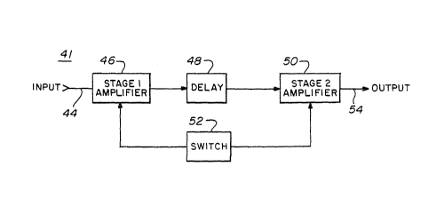
Referring to the drawings and more particularly to
FIGS. 4 and 5 there may be seen the block diagram of the
sequential amplifier of the present invention. The
sequential amplifier 41 consists of at least two stages, 46
5 and 50. A delay device 48 is placed between the amplifier
stages 46 and 50 and a switch 52 is used to control
adjacent amplifier stages in the proper sequence. A delay
line may be constructed from a variety of well-known
devices such as a surface acoustic wave device.
Each amplifier stage may be similar in design and
construction. However, this is not essential. The
requirement for each amplifier stage is that it not
generate an output that causes oscillations with adjacent
stages. Thus, the most simple and straightforward manner
15 of achieving this result occurs when each stage amplifies
or provides gain to an input signal when it is energized
and the other stage or stages operating at the same
frequency are de-energized.
The switching unit depicted in FIG. 4 will control
20 adjacent amplifier stages so that, in the preferred
embodiment, no two amplifier stages are energized
simultaneously. A switch may be constructed from among a
variety of well-known devices including clocks or bistable
multivibrators.
As can be seen in FIG. 4, an input signal on terminal
44 is coupled to an amplifier 46 which may be considered to
be the first stage amplifier. The output signal from the
amplifier 46 is coupled to a delay line 48. The output of
the delay line 48 is coupled to a second amplifier 50 which
may be considered to be the second stage amplifier. The
output of the second stage amplifier is coupled to an
output terminal 54. In this embodiment, the switch 52
operates such that the first stage amplifier 46 is
212~7~ ~
turned ON and the second stage amplifier 50 is turned
OFF for a predetermined period of time. Assume, for
example only, that the delay 48 has the delay time of
one microsecond. The switch 52 may then turn ON the
stage 1 amplifier 46 for a predetermined period of
time, such as, for example only, one microsecond.
Switch 52 then turns OFF the stage 1 amplifier 46
and, as the amplified signal is emerging from the one
microsecond delay line 48, switch 52 turns ON the
second stage amplifier 50 which again provides an
amplification to the RF signal. Thus, for this
embodiment, at no time are the first and second stage
amplifiers ON simultaneously.
The amount of delay provided by the delay line 48
and the time at which switch 52 turns the first and
second stage amplifiers 46 and 50, respectively, ON
and OFF may be varied. This timing relationship is
illustrated with reference to FIGS. 8 and 9. In FIG.
8(a), the width of the waveform (shown with shading
for clarity) indicate9 the time that the stage
amplifier is ON or energized. In waveform (b), the
shaded area represents the delay time of the delay
line. In waveform (c), the shaded area represents
the time of energization of the stage 2 amplifier.
2s Thug it i9 noted in FIG. 8 that the stage 1 amplifier
46 may be ON for some given period of time, such as
one microsecond for example only. The delay line may
also have a given delay time, such as one
microsecond, as illustrated. Thus, when the
amplifier 46 in stage 1 is energized or ON, the
output signal is coupled to the delay line and
emerges from the delay line after the one-microsecond
delay and at that time the stage 1 amplifier is
2 1 h,l L~ 7 l ~
de-energized or turned OFF and the stage 2 amplifier
is energized or turned ON to receive the output
signal from the delay line 48.
As can be seen in FIG. 9, the time period of
energization of the stage 1 amplifier as illustrated
in waveform (a) may be some fraction of the delay
line time period, such as one-half microsecond while
the delay line may have a larger delay time period
such as one microsecond as shown in waveform (b).
However, when the amplified signal from the first
amplifier stage 46 passes through the delay line 48
and emerges therefrom, the second stage amplifier 50
is turned ON and amplifies the output signal. It is
noted in FIG. 9 that the stage 1 amplifier 46 is
de-energized long before the signal emerges from the
delay line. Clearly, the times given are for
illustration purposes only. For instance, the width
of the illustrated waveforms in (a), (b) and (c) of
FIG. 8 could be two microseconds, five microseconds
or any other time as desired. In like manner, the
waveforms illustrated in FIG. 9(a), (b) and (c) could
be one-quarter microsecond and one-half microsecond,
respectively, for waveforms (a) and (b). They could
be one microsecond and two microseconds for waveforms
(a) and (b). In other words, the time delay can be
selected to meet the needs of a particular
situation. For example, the stage 1 amplifier ON
time may be greater than the delay time as shown in
FIG. 10 where the stage 1 amplifier ON time is X and
the delay line delay time is 3/4X, for purposes of
explanation and example only. The signal from the
stage 1 amplifier as shown in FIG. 10(a) exits the
delay line 3/4X later, the time period shown in FIG.
10(b) by the letter "a", and 1/4X before stage 2
-- 2 1 2 Ll 7 ~ 8
turns ON as shown in FIG. 10(c) by the letter "b". When
all of the stored signal has exited the delay line (FIG.
10(c)), the second stage amplifier is still ON as shown by
the letter "c" but no signal is present. The timing then
repeats itself. The first amplifier stage amplifies the
signal for a full period, X, while the second amplifier
stage amplifies the signal for a period of 3/4X. That
portion of the signal exiting the delay line before
amplifier 2 is turned ON is lost. The essential
requirement in this embodiment is that both of the first
and second stage amplifiers 46 and 50 cannot be ON or
energized simultaneously. With the circuit 41 operating in
this manner, the first amplifier stage 46 can amplify the
RF signal to its maximum capability. Although the signal
may be radiating and/or being conducted to the second stage
amplifier 50, that amplifier is OFF and consequently there
are no adverse effects. In like manner, when the second
stage amplifier 50 is amplifying the signal to its maximum
capability, it is also radiating the RF signal. However,
because the first stage amplifier 46 is then turned OFF,
there is no adverse effect. Thus maximum gain can be
obtained in the RF stages where the gain is most difficult
to obtain. It is to be understood, of course, that the
circuit 41 shown in FIG. 4 can be used with any desired
frequencies from audio to UHF. Even in audio stages, if
the amplifier stages are driven sufficiently hard,
radiation and/or conduction can occur from one stage to
another at audio frequencies. Thus, the circuit can be
used with any frequency so long as the amplifier stages are
not energized simultaneously.
FIG. 5 is a general representation of a circuit
utilizing the present invention and having three
-
~171~
stages of gain. As can be seen in FIG. 5, an input signal
on line terminal 55 is coupled to an amplifier 56, the
first stage amplifier. Its output is coupled to the first
delay line 58 and the output of the delay line 58 is
coupled to a second amplifier stage 60. The output of the
second amplifier stage 60 is coupled to a second delay line
62 that has its output coupled to the third amplifier stage
64. The output terminal 66 is coupled to and receives the
output from the third amplifier 64. A clock or a bistable
multivibrator 68 may be used to generate timing signals on
lines 70, 72 and 74 at any desired interval in a well-known
manner. When the clock 68 generates a first signal on line
70, only the first amplifier stage 56 is energized. It
amplifies the input signal and couples it to the delay line
58. In one embodiment, when the first stage amplifier 56
is shut OFF by the clock pulse line on line 70, the clock
generates a second pulse on line 72 which turns the second
amplifier stage 60 ON when the signal exits from the delay
time of delay line 58. Of course, the gating may be such
that second amplifier stage 60 is turned ON before, or
after, the signal exits from delay line 58 as explained
previously. The second amplifier stage 60 then receives
the delayed amplified signal from the delay line 58 and
amplifies it. In this embodiment, clock 68 then removes
the signal from line 72 and de-energies amplifier 60.
Clock 68 then provides the clock signal on line 74 that
energies amplifier 64, the third stage amplifier. It
receives the amplified output from delay line 62 and
generates the output on line 66. Thus three stages of
amplification are provided in FIG. 5. Again, it will be
noted that only one of the amplifiers 56, 60 and
64 is energized at any one time. Thus while each of
the amplifiers 56, 60 and 64 is radiating signals
when it is energized, the radiations are not a
detrimental influence on the remainder of the system
because any two of the amplifiers are de-energized
during the time the third amplifier is energized and
thus the de-energized amplifiers do not accept the
radiated signals.
FIG. 6 is a circuit similar to that in FIG. 5
except that a monostable multivibrator 90 is used to
energize the first amplifier 78 for a predetermined
period of time with an enabling pulse on line 92.
When the enabling pulse on line 92 decays, the
amplifier 78 is de-energized and the trailing edge of
lS the pulse on line 94 then energizes multivibrator
96. Again, an enabling pulse is produced on line 98
to energize the second stage amplifier 82 for a
predetermined period of time. When the pulse on line
98 is removed, the trailing edge of the pulse causes
a signal on line 100 that energizes the third
multivibrator 102. Again, an enabling pulse is
generated on line 104 that energizes amplifier 86,
the third stage amplifier. At the time when the
third ~tage amplifier 86 is de-energized, the
trailing edge of the pulse from multivibrator 102 on
line 106 energizes the first multivibrator 90 and the
cycle repeats itself. Clearly there may be other
arrangements that could be used, but in any case with
this embodiment the limiting factor is that only one
of the three amplifiers in FIGS. 5 and 6 may be
energized at any one moment in time.
A typical application of the sequential amplifier
is shown in FIG. 7. Here the sequential amplifier 41
is included in a receiver such as a radio receiver or
2~2~7~
18
a TV receiver. The antenna 108 receives a modulated
radio frequency signal that is coupled to and
filtered by a tunable or nontunable filter such as a
coupled resonator filter 110 to select and isolate
S the modulated RF signal. The sequential amplifier 41
is shown in phantom lines, and is a duplicate of the
circuit of FIG. 4. It will amplify the selected
input RF signal as previously described. The
amplified RF signal will then pass through the
detector 112 that, in combination with device 114,
will detect and demodulate the signal. The device
112 may be a frequency discriminator for FM signals
or an AM detector for AM signals. The low pass
filter 114 removes the enabling or switching pulses
as well as the RF carrier as is well known by those
skilled in the art. The detected signal will
essentially be the audio component of the received
radio signal. The detected signal will then pass
through an audio amplifier 116 and then into the
audio output device 120. The output power of the
sequential amplifier may be adjusted by means of an
automatic gain control (AGC) 118 for AM circuits as
desired.
FIGS. 11 and 12 illustrate two possible alternate
timing relationships between stages as the preferred
embo~lmPnt of this application, wherein both the
first and second stages may be energized at a given
time to achieve maximum gain for so long as no
feedback occurs to cause interference between
amplifier stages. The block diagram for such a
circuit is similar to that shown in FIG. 4. This
embodiment is feasible because of the delay
introduced by the delay device 48. This delay
provides a period of time before feedback effects
- 2~ 8
19
between simultaneously energized adjacent stages will
produce unwanted oscillation. The typical
configuration for such an embodiment would therefore
require that the first stage be de-energized j USt
prior to the point where circuit oscillation occurs.
Thus, in FIG. 11 there is depicted, for example
only, a situation where both first and second stages
are energized for an equal duration, with an overlap
between the energization of both stages shown in
areas with hatched lines. In FIG. 12, there is
depicted a situation where the first stage is
energized for a shorter period than the second stage,
again with an overlap wherein both stages are
simultaneously energized as shown by the areas with
hatched lines. In either case the limiting factor is
that the first stage may remain energized while the
second stage is also energized only for so long as
oscillation does not occur due to feedback effects
between stages. Naturally, this point where
oscillation occurs will vary depending on many
factors, including the particular circuit components
and frequencies chosen. It must also be noted that
this embodiment is also useful in multiple amplifier
stage systems.
One skilled in the art will recognize that the
alternate energization of the amplifiers is a form of
sampling of the input signal. It will be understood
that the sampling rate can be greater than or less
than the modulation signal frequency. Thus with a
high sampling rate there would be a large number of
samples per cycle of the modulation signal. With a
low sampling rate, there would be a large number of
modulation cycles per sample.
2~2~ 3
Thus, there has been disclosed a novel sequential
amplifier that can be used to amplify electronic
signals of any type where radiation or coupling of
the signals from one stage by other means could cause
feedback to a previous stage and thus limit the
amount of stable amplification that can be achieved.
As can be seen from the above description, the
sequential amplifier is ideally suited for use in
radio receivers. Note, however, that this type of
circuit has many applications. It could be used to
amplify signals in a transmitter, for instance. This
circuit may be employed almost anywhere electronic
signal amplification is needed.
The circuit can be used with signals such as AM,
FM, PPM, PCM, FSK, digital signals, analog signals
and other like signals that need to be amplified.
While the invention has been described in
connection with a preferred embodiment, it is not
intended to limit the scope of the invention to the
particular form set forth, but, on the contrary, it
is intended to cover such alternatives, modifica-
tions, and equivalents as may be included within thespirit and scope of the invention as defined by the
appended claims.