Note: Descriptions are shown in the official language in which they were submitted.
2I2474~
FIELD OF THE INVENTION
This invention relates to the field of logic
circuits, and in particular to a CMOS to ECL logic
converter.
BACKGROUND TO THE INVENTION
High speed electronic logic systems are often
comprised of a mixture of silicon integrated circuit
(IC) technologies. A system may be formed of
complementary metal oxide silicon (CMOS) field effect
transistors (FETs), transistor-transistor logic (TTL)
transistors, or emitter coupled logic (ECL) devices. A
system designer will choose the best silicon IC
technologies, in terms of cost or performance, for each
function of the system being designed. For example,
medium to low-speed computational functions have been
found to be better implemented in CMOS, high speed
serial functions have been found to be better suited for
ECL, and TTL is used where moderately high-speed is
required but the extra complexity of ECL is not
warranted.
Connecting sub-systems that use all of these
silicon technologies is difficult. A CMOS to ECL
interface poses a particular challenge, because of
differences is logic voltage swings and power supplies.
Typically, CMOS logic voltage swings between +5 volts
for a logical "1" and 0 volts for a logical "0". On the
other hand, ECL data signals swing between -0.8 volts
for a logical "1" and -1.8 volts for a logical "0".
CMOS devices are nominally powered with a 5 volt supply,
and ECL devices are powered with a -4.8 to -5.2 volt
supply. Therefore, the system designer has power
supply, voltage swing, and logic level reference level
problems when an attempt is made to create CMOS to ECL
interfaces in a design. CMOS output signals must be
translated to be suitable for use with standard ECL
devices.
Part of these problems can be solved if the
system designer chooses to power ECL devices with the
same 5 volt power supply used for the CMOS and TTL
devices. The VCC terminal of the ECL circuit is
connected to 5 volts, and its VEE terminal is connected
to the system ground. While ECL devices are very
susceptible to noise on their VEE rail, if this rail is
decoupled well and if differential devices are used,
this powering scheme has been found to be tractable.
A remaining problem, however, is to create a
CMOS output with logical swings that match that of an
ECL device relative to the 5 volt, or VDD supply rail.
In the article "ECL-CMOS and CMOS-ECL Interface
in 1.2~m CMOS for 150-MHz Digital ECL Data Transmission
System", IEEE Journal of Solid-State Circuits, Vol 26,
No. 1, January 1991, by Michael S.J. Steyaert, et al, a
circuit is described in which high speed current
switches are controlled by a replicated bias scheme.
However this circuit requires an external termination
voltage supply, and its output driver has been found to
be unstable under some conditions.
SUMMARY OF THE INVENTION
The present invention is a system for
converting CMOS logic signals to ECL logic signals,
which, while using a replicated bias scheme similar to
the one of Steyaert et al, requires no external
termination voltage supply, and which has been found to
be stable under all conditions. A single voltage
supply, which can be the same one powering the CMOS
circuits and the ECL circuits, can be used to power the
circuits of the present invention. The present invention
can be configured with two external resistors for each
data channel for different termination values and
2
CA 02124745 1998-04-03
logical swings, and is designed to track changes over
process, supply rail and temperature.
A successful laboratory prototype contains a
pseudo-ECL transmitter (PETX) which receives two single-
s ended input signals, a high speed digital clock stream (<_
155 MHz) and a high speed data stream (<= 77.5 MHz) and
transmits two fully differential ECL voltage swing
compatible output signals. These output signals can be DC
coupled to board-level ECL devices when they are biased
between 5V and ground in a pseudo-ECL mode.
In accordance with an embodiment of the
invention, a complementary metal oxide silicon (CMOS) data
to emitter coupled logic (ECL) data translator system is
comprised of a translator circuit for receiving data
signals from a CMOS circuit, the translator circuit and
CMOS circuit powered from a CMOS voltage power source, a
circuit for powering an ECL circuit from the power
source, a transmission line carrying output signals from
the translator circuit to the ECL circuit, having a
predetermined characteristic impedance, a load having the
characteristic impedance connecting the transmission line
to the power source, and the translator circuit comprising
a circuit for outputting a data signal on the transmission
line which corresponds to the received data signals but
having an amplitude compatible with the ECL circuit and
referenced to a voltage of the power source.
In accordance with another embodiment, the
translator circuit is comprised of a one bit digital to
analog converter (DAC) and is further comprised of a pair
of programmable current steering switches connected to the
DAC for establishing higher and lower output currents for
opposite logic values of the output signals, a circuit for
applying the data signals to the DAC and for receiving the
output signals and applying them to the transmission line.
3
CA 02124745 1998-04-03
BRIEF INTRODUCTION TO THE DRAWINGS
A better understanding of the invention will be
obtained by reading the description of the invention
below, with reference to the following drawings, in which:
Figure 1 is a general block diagram of an
embodiment of the system invention,
Figure 2 is a block diagram of a preferred
embodiment of the translator (PETX) of the system,
Figure 3 is a block diagram of an ECL CORE
circuit 16, used in the translator or Figure 2,
Figure 4 illustrates a bootstrap circuit used in
the ECL CORE circuit of Figure 3,
Figure 5 is logic diagram of the phase splitter
described with reference to Figure 4,
Figure 6 is a block schematic of the ECL SUB3
circuit described with reference to Figure 3,
Figure 7 is a schematic diagram of a programmable
current steering switch in the ECL SUB3 circuit described
with reference to Figure 3,
Figure 8 is a block diagram illustrating a
circuit for generating the control voltages VA and vB,
DETAILED DESCRIPTION OF THE INVENTION
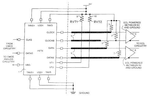
Figure 1 illustrates the invention in broadest
concept. A translator, which will be referred to below as
a PETX (pseudo ECL transmitter), translates single-ended
signals received from CMOS circuitry, shown as clock
signals applied to a CLKS input and data signals applied
to a DATAS input, into fully differentiated signals for
application to ECL circuits 3. The signals for
application to the ECL circuits are output from the PETX 1
to transmission lines 5, which have predetermined
characteristic impedances, from differentiated clock
signal output terminals CLOCK and CLOCKB, and data signal
output terminals DATA and DATAB.
4
212474
Load resistors 7 terminate each of the
transmission lines 5, in a well known manner. For
example if the characteristic impedance of the
transmission lines is 100 ohms, the resistance of each
load should be 100 ohms.
Various power inputs of the PETX TAVD1, VDD1
and TAVD are connected to 5V, the 5 volt power supply
terminal that supplies the CMOS circuits from which the
CMOS circuits are powered, and supply terminals TAVS1,
VSS1 and TAVS are connected to ground. The load
resistors are also connected to 5V, as are the ECL
circuits.
As noted earlier, it is a requirement of this
invention to provide digital signals corresponding to
the input signals from the CMOS circuits which normally
output logic signal voltage values between +5 volts for
a logical "1" and 0 volts (ground) for a logical "0", to
logic signal voltage values that can be received and
translated properly by the ECL circuits, which logic
voltage values are normally between -0.8 volts for a
logical "1" and -1.8 volts for a logical "0". CMOS
circuits are nominally powered with a 5 volt power
supply, and ECL circuits are powered with a -4.8 to -5.2
volt supply.
As noted above, the ECL circuits are powered
from the same 5 volt supply as is the CMOS circuits.
Thus the present invention must translate the input CMOS
logic levels to the correct logic voltage values, and
with a similar voltage swing (i.e. 1 volt) but at the
correct reference level to accommodate the power supply
reference level used by the ECL circuits.
The preferred embodiment of the present
invention uses a 1 bit digital to analog converter
(DAC), to be described in more detail below, which
converts a CMOS input signal into differentiated output
5
CA 02124745 1998-OS-06
signals, and a pair of programmable current steering
switches connected to the DAC to establish higher and
lower logic level output currents for the opposite logic
values of the output signals.
The steering circuits are programmed by means
of two resistors 9 and 10 connected to 5V and
respectively to VT1 and VT2 terminals of the PETX, which
will be referred to below as resistors RVT1 and RVT2
respectively. The values of these resistors are
determined according to the following equations:
RVT1 = 2*KVT1*RL/VPOH and
RVT2 = 2*KVT2*RL/VPOL
where
KVT1 = 7.12
KVT2 = 6.282
VpOH is the ECL compatible high logic level
output voltage (referenced to TAVD, connected to 5V),
and
-1.0 <= VpOH <_ -0.8
-1.8 <= VpOL <_ -1.6
RL is the characteristic impedance of the
transmission line, e.g. 100 ohms.
The above provides a translation system that
both translates CMOS logic signals into pseudo-ECL logic
signals, references them to a single power supply, the
power supply of the CMOS circuits, and provides for the
ECL circuits to be powered from the same power supply as
the CMOS circuits. Further, the output transmission
lines are terminated be loads connected to the same
power supply. Both the high and low logic voltage
levels of the pseudo-ECL logic signals can be
controlled, and referenced to the same power rails to
which the CMOS circuits and the ECL circuits are
connected. The result is a stable mixed-CMOS and ECL
system which can provide improved cost and performance
6
212474
of such a system, and gives the designer increased
design flexibility.
A better understanding of the structural
location of the DAC and programmable current steering
switches will be obtained after the architecture of the
system is described.
With reference to Figure 2, a block diagram of
the PETX 1 is shown. While the circuit can be
constructed to translate only one data signal, it will
be described translating two signals, a clock signal
CLKS and a data signal DATAS. The PETX receives CMOS
clock and data signals at inputs CLKS and DATAS of
drivers 13, 14 (formed of CMOS field effect transistors
FETs), which buffer the CMOS logic signals (improving
the signal shapes), and which apply the resulting
signals to CLKIN and DATAIN inputs of an ECL CORE
circuit 16. The ECL CORE circuit is a high speed, 1-bit
digital to analog converter (DAC).
An ECL BIAS circuit 18 is connected to the ECL
CORE circuit 16, and adjusts the ECL CORE reference
voltages VA and VB dynamically over variations in
temperature, supply voltage and of the production
process. The aforenoted resistors RVT1 and RVT2 between
the 5V supply and the VT1 and VT2 terminals establish
the operating points for the nodes to which the voltages
VA and VB are connected.
The three groups of power supplies connected to
the terminals noted with reference to Figure 1 provide
the following: TAVD1 and TAVS1 supplies the ECL BIAS
circuit 18, TAVD and TAVS supplies the high current
sections of the ECL CORE circuit 16, and VDD1 and VSS1
supplies the high speed logic portion of the ECL CORE
circuit 16.
Outputs of the ECL CORE circuit are the
differentiated pseudo-ECL logic signals: the clock
7
' 212474
output signals CLOCK and CLOCKB, the data output signals
DATA and DATAB, and the pseudo-ECL output signal logic
level programming terminals VT1 and VT2.
Figure 3 illustrates a block diagram of the ECL
CORE circuit 16. The ECL CORE circuit is comprised of
bootstrap circuits 20 and 21, each for signal splitting
the respective CMOS input signals CLKIN and DATAIN
received from the drivers 13 and 14, into fully
differentiated pseudo-ECL output pairs of signals into a
delayed in-phase CMOS signal and a delayed 180 degree
out-of-phase CMOS signal, and waveshapes them. The
output resulting differentiated signals are OUT and
OUTB.
These signals are applied to respective
terminals of an ECL SUB3 circuit 23 as follows. The
output signals of bootstrap circuit 20 are applied to
CLK and CLKB input terminals of the ECL SUB3 circuit,
and the output signals of the bootstrap circuit 21 are
applied to DATA and DATAB input terminals of the ECL
SUB3 circuit.
In addition, output terminals OUTBS and OUTBBS
of bootstrap circuit 20 are internally capacitively
coupled by means of capacitors 25 and 26 respectively to
output terminals OUT and OUTB, and output terminals
OUTBS and OUTBBS of bootstrap circuit 21 are internally
capacitively coupled by means of capacitors 27 and 28
respectively to output terminals OUT and OUTB of
bootstrap circuit 21. The signals carried by the OUTBS
and OUTBBS terminals are used as bootstrap signals as
will be described below.
The ECL SUB3 circuit is comprised of an array
of current steering elements referred to earlier, and
provides differentiated clock and data output signals at
terminals CO, COB, and DO, DOB respectively, which
8
212474
.._
correspond to the CLOCK, CLOCKB, DATA and DATAB
terminals in the description of Figure 1.
Wave-shaping is performed based on the charge
conservation principle. The terminals CO, COB, DO and
DOB have large capacitive loads, as a result of
integrated circuit pin, diffusion and internal metal
parasitic capacitance. The output voltage swing
expected at these terminals is small, nominally one
volt. In order to improve this voltage swing and make
it more robust, the bootstrap signals described above
which are in phase with the signals carried on the
output terminals are applied to those output terminals,
i.e. the signals from OUTBS of bootstrap circuit 20 to
output terminal CO, the signals from OUTBBS of bootstrap
circuit 20 to terminal COB, the signals from OUTBS of
bootstrap circuit 21 to terminal DO and the signals from
OUTBBS of bootstrap circuit 21 to terminal DOB.
The coupling capacitors 25, 26, 27 and 28
supply the charge required to drive the output parasitic
capacitive loads, and can be much smaller than these
parasitic capacitive loads because of their much larger
drive.
The value of each bootstrap capacitor 25, 26,
27 and 28 Cbs can be calculated by the following
equation:
Cbs * (dVin - dVout) - Cp * (dVout)
where Cp is the parasitic load capacitance at
an output CO, COB, DO and DOB,
dVout is the output voltage swing, and
dVin is the bootstrap voltage swing.
Typical values for dVin, dVout and Cp are 5 volts, 1
volt and 10 pf respectively. In this case a nominal
value for Cbs is 2 pf.
Figure 4 illustrates one of the identical
bootstrap circuits 20 and 21. This circuit is comprised
9
212474
of a tapered buffer 30, which receives a CLKIN or DATAIN
signal at its IN terminal and applies its output signal
to the IN terminal of a high speed phase splitter 32.
The phase splitter splits its input signal into two
signals SB and S, and applies them to the terminals OUT
and OUTB, with the signal carried by terminal OUTB 180
degrees out of phase with the signal carried by terminal
OUT. Capacitors 25 and 26, for example, carry the
signals from terminal OUT and oUTB respectively to
terminals OUTBS and OUTBBS.
The signal presented to the bootstrap circuits
have been found to suffer a substantial amount of
degradation due to the substantial distance between
input cell elements. The tapered buffer 30 ensures that
the signal input to the phase splitter 32 has a short
ramp time, e.g. less than 1 ns. This is important if
low duty-cycle distortion and a robust eye-pattern for
the pseudo-ECL output signals is desired.
The phase splitter is formed of two exclusive
OR (XOR) gates in a circuit as shown in Figure 5. The
input is applied to one input of each of two XOR gates
34 and 35. The other input of gate 34 is connected to
power terminal TVDD and the other input of gate 35 is
connected to the return (ground) terminal TVSS. The
output terminal SB and S of the XOR gates 34 and 35
provide the phase split signals for application to
terminals OUT and OUTS.
This phase splitter circuit is preferred
because it provides symmetrical propagation delays for
high/low or low/high input transitions, and thus ensures
low output signal skews. The output of the phase
splitter should be able to drive a 15 pf load, and the
tapered buffer in the XOR output will facilitate this
loading.
2i2~74~
The ECL SUB3 circuit 23 will now be described
with reference to Figure 6. Each of the DATA, DATAB,
CLK and CLB signals is applied to an array 37 of ten ECL
TX2 elements, all of the elements in each array
operating in parallel. The outputs of the arrays are
respectively DO, DOB, CO and COB, described with
reference to Figure 2. A single grouping of ten
elements constitutes a 1-bit, high speed DAC.
In addition, two arrays each of two ECL TX2
elements generate internal bias voltages VA and VB. The
output (logic) current levels are controlled by the bias
voltages VA and VB, which are in turn affected by the
voltages applied via the external resistors 10 (Figure
1)to their VT1 and VT2 terminals, described earlier,
which pull the VT1 and VT2 terminals to the positive
voltage supply rail 5V.
Reference is now made in addition to Figure 7,
which is a schematic diagram of an ECL TX2 element,
which is a programmable current steering switch. The
voltages VA and VB, generated by the two 2 element
arrays, are applied to the respective gates of FETs 39
and 40, the sources of which are connected to the TAVS
ground terminal. The drain of FET 40 is connected to
the source of FET 42, and the drain of FET 39 is
connected to the source of FET 41. The drain of FET 42
is connected to the TAVD power terminal, and the drain
of FET41 is connected to the source of FET 42. That
point is also connected to the gate of FET 43, the
source of which is connected to ground terminal TAVS,
and the drain of which is connected to the OUT terminal.
The gate of FET 41 is designated as the IN terminal.
The OUT terminal of each array is connected to
the DO, DOB, CO and COB terminals respectively (see
Figure 6).
11
In operation, if the signal at the IN input is
a logical "1", the voltage at the gate of FET 43 is low
due to FETs 41 and 39 conducting, drawing the voltage at
gate 43 low relative to voltage TAVD. As a result, FET
43 does not conduct, and the output current passing
through the source-drain circuit of FET 43 and through
the load resistor connected to the OUT terminal (see
Figure 1) is at a minimum value. Therefore the voltage
drop across the load resistor is at a minimum, and a
logic "1" voltage is appear across the transmission line
to the input of the ECL circuit to which it is
connected.
In a similar manner, when a logical "0" appears
at the input terminal IN, the voltage at the gate of FET
43 is high due to FETs 41 and 39 being switched into
their non-conductive states, and FET 43 conducts,
drawing maximum current through its source-drain circuit
and the load resistor connected the OUT terminal, thus
causing high current, and thus a high logic level
voltage to appear across the transmission line to the
input of the ECL circuit.
The voltage level of the control signals VA and
VB applied to the gates of FETs 39 and 40 respectively
control the threshold of conduction of FETs 39 and 40,
and therefore the threshold of conduction of the series
of FETs 39 and 41, and FETs 40 and 42 respectively.
Thus the control signal VA determines the level of
current carried by FET 43 for a logical "0" and logical
"1" respectively, and thus the current and voltage for
these states in the load resistor.
The voltages VA and VB thus are important to
determine the pseudo-ECL logical voltage levels. These
voltages are generated by the ECL TX2 circuits in the
two arrays 45 and 46 (Figure 6). With reference to
Figure 8, the voltages VA and VB are generated in two
12
feedback loops each using two ECL TX2 cells. The
inverting input of an operational amplifier 48 is
connected to VT2, and its non-inverting input to an
internal reference designated by VDRL. The output of
operational amplifier 48 is VB1. Similarly, the
inverting input of operational amplifier 49 is connected
to VT1 and its non-inverting input to an internal
reference designated by VDRH. Its output is VB2.
The two ECL TX2 circuits have their IN inputs
tied to logical "0". The internal voltage reference
circuit can be of well known form, e.g. a bandgap supply
driving an operational amplifier, which is connected to
the gate of FETs 51 and 52, and should be temperature
compensated and create a constant 2 volts below the
positive rail (due to the operational amplifier's
virtual ground), and should be constant over process
and temperature. The voltage references are comprised
of resistors 54, 55 and 56,57 connected in series with
the source-drain circuits of FETs 51 and 52
respectively, between the TAVD and TAVS terminals. This
dynamically determines the value of VB for all the ECL
TX2 circuits, and hence the logical "0" output current
level. The voltage VA is determined in a similar
fashion, but the ECL TX2 circuits have their inputs IN
tied to a logical "1", and the terminals VT1 and VA are
used in a separate feedback loop from the one described
above.
The VA and VB control voltages are thereby
produced in arrays 45 and 46, and are supplied to the
arrays 37, which operate as described earlier.
It should be noted that the application of a
"0" state to the gate of FET 43 determines the output
logical "0" current level. The determination of this
state in no way depends on the value of VA. If there is
a "1" state applied to the gate of FET 43, an output
13
logical "1" current level results. The value of VA in
this case is dependent on the value of VB, but since the
feedback loops that determine there control voltages are
separate, the dynamics of VA and VB are not coupled.
Since the current sunk into the VT1 and VT2
terminals control, with the VDRL and VDRH voltages, the
outputs of operational amplifiers 48 and 49, these
currents uniquely determine the potentials VA and VB.
Changing the termination resistors 10 (Figure 1) between
terminals VT1 and VT2 and the positive supply adjusts
the VA and VB voltages, and the DACs logical "low" and
"high" output levels.
A person understanding this invention may now
conceive of alternative structures and embodiments or
variations of the above. All of those which fall within
the scope of the claims appended hereto are considered
to be part of the present invention.
14