Note: Descriptions are shown in the official language in which they were submitted.
2124773
BACKPLANF~ AND S~T'.T.F
The present invention relates to computer backplane
arrangements and is particularly concerned with
telecommnnications applications thereof.
Back~round to the Invention
It is well known in the computer industry to use a
backplane bus arrangement with a plurality of circuit cards.
Each circuit card plugging ingto a female connector mounted
on one surface of the backplane. One such computer bus
arrangement is the IEEE standard 1014-1987 VMEbus. The
VMEbus is an industry standard multiprocessor system bus
that uses a 32-bit address and data bus for communication
between various VME cards. Because of the success of this
standard and the availability of circuit cards for use
therwith, it is highly desirable to use this standard in
industries whose standard practices are at variance with
those of the computer industry. In particular, the
application of the VMEbus to telecommunication is hindered
by industry guidelines on maintenance and safety, for
example NEBS (BellCore TR-NWT 000063).
Summary of the Invention
An object of the present invention is to provide and
improved backplane and shelf arrangement.
In accordance with an aspect of the present invention
there is provided a backplane for a computer comprising: a
printed circuit board having first and second faces and
first and second busses; a plurality of first connectors
disposed upon the first face, distributed along the
backplane at a substantially fixed interval spacing and
connected to the first bus; a plurality of second connectors
disposed upon the first face, distributed along the
backplane at a spacing similar to the spacing of the first
connectors, and connected to the second bus, each of the
first and second connectors are substantially aligned across
the backplane to define a respective slot; and a plurality
of third connectors disposed upon the second face,
distributed along the backplane at a spacing similar to the
212~773
-
spacing of the second connectors, each third connector
offset from a respective second connector along the
backplane by approximately one-half the spacing of the
respective second connector.
Advantages of the present invention are a simplified
more space efficient shelf and bus arrangement which remain
compatible with standardized cards and modules.
Brief Descri~tion of the Drawinas
The present invention will be further understood from
the following description with reference to the accompanying
drawings in which:
Fig. 1 illustrates in a block diagram a bus arrangement
in accordance with the IEEE VMEbuS standardi
Fig, 2 illustrates in a partial plan view of a known
VMEbus backplane and shelf arrangement;
Fig. 3 illustrates in a partial plan view of a VMEbus
backplane and shelf arrangement in accordance with an
embodiment of the present invention;
Fig.4 illustrates in a plan view the backplane of Fig.
3; and
Fig. 5 illustrates in a plan view the shelf arrangement
of Fig. 3.
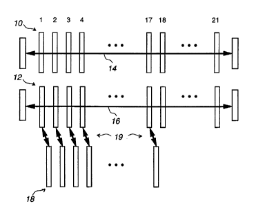
Referring to Fig. 1 there is illustrated in a block
diagram a bus arrangement in accordance with the IEEE VMEbus
standard. The VMEbus is an industry standard multiprocessor
system bus that uses a 32 bit address and data bus for
communication between various VME cards. The VME standard
bus provides as a maximum number of 21 VME card slots. The
VMEbus includes two rows 10 and 12 of female connectors
providing access to so-called VME P1 and VME P2 busses 14
and 16, respectively. The VMEbus backplane provides female
connectors 10 and 12 on the front face for receiving
standard VME cards in slots 1 through 21. The VMEbus also
provides male connectors 18 on the back side of the
backplane for each slot. Male connectors 18 are used to
couple VME cards (not shown in Fig. 1) to corresponding
transition cards via ribbon cables (not shown in Fig. 1 but
-~12~7~
indicated by arrows 19). The VME transition cards are used
for the connection of the shelf to other systems through
interfaces such as ethernet, and SCSI bus for disk drives.
Referring to Fig. 2 there is illustrated in a partial
plan view, a known VMEbus backplane and shelf arrangement.
A backplane 20 includes on its front face the plurality of
female connectors 12 each for receiving a corresponding male
connector 22 mounted on a respective circuit card 24. The
circuits cards 24 each have faceplate 26 attached to the
front edge thereof. Pins of female connectors 12 extend
through the backplane 20 to form male connectors pins of
male connector 18. Each card in the slot so provided can be
connected to a transition card 28 via a male connector 30
and ribbon cable 32 having female connectors 34 and 36 at
each end thereof.
For the computer industry the standard VMEbus
arrangement is acceptable practice. Other desired
applications for the VMEbus, however, may have in place
restrictions that can not be accommodated by the standard
VMEbus arrangement. For example, in the telecommunications
industry compliance with industry guidelines such as NEBS
(BellCore TR-NWT 000063) prevent the direct application of
standard practices from other industries such as the
computer industry.
Referring to Fig. 3 there is illustrated in a partial
plan view of a VMEbus backplane and shelf arrangement in
accordance with an embodiment of the present invention. A
backplane 40 includes, on its front face, the two rows of
female connectors 10 and 12 which connect cards to the VME
P1 and P2 busses as in Fig. 2 lonly connectors 12 are shown
in Figs. 2 and 3). On the back of backplane 40 there is a
row of female connectors 42 offset from and interconnected
with corresponding female connectors 12. Typically, each of
the 21 card slots is interconnected to corresponding female
connectors 42.
The backplane 40 provides the backbone for all of the
cards that are used in the VMEbus system. This includes the
2124773
21 slot VMEbus (connectors Pl and P2) of the main system
backplane for VME cards and transition card connectors 42 on
the back of backplane 40 that are connected by the backplane
directly to the P2 connectors 12 of VME cards for the first
17 slots.
Referring to Fig. 4 there is illustrated in a plan view
the backplane of Fig. 3. The 21 VME card slots 44 are
defined by the placement and spacing of two rows of female
connectors 10 and 12, on the front of the backplane 40. The
two rows of female connectors 10 and 12 provide connection
to the so-called VME Pl and P2 busses, respectively.
Connectors on the back of backplane 40 are illustrated in
broken line. These include the female connectors 42 for
connection to the transition cards 28 and additional female
connectors 46 for power connections to transition cards 28.
The 21 slot VMEbus is the primary bus on the backplane
and it is connected between the 21 card slots on the bus.
This bus is carried on 128 pins of two separate connectors
as shown in Tables A and B. The VMEbus uses all 96 pins on
the top connector referred to as the Pl connector in the
VMEbus standards while it uses only the middle 32 pins (row
B) of the second connector referred to as the P2 connector.
The signals on each of these connectors can be divided
into three separate groups with regards to the tracking on
2 5 the backplane between the connectors. These groups are:
power and ground; bus signals; and daisy chain signals. The
tracking of all these signals is performed according to the
VMEbus standard referred to herein above.
The power and ground signals are all connected directly
to the power and ground planes on the backplane at each of
the pins.
The daisy chain signals include the 8 bus grant signals
(BGOIN*~ BGOOUT* through BG3IN* and BG30UT*) that appear on
row B of the Pl connector in Table A. Also the interrupt
acknowledge (IACKIN* and IACKOUT*) signals that are on row A
of the Pl connector. These five signals are connected to
form a daisy chain across the bus with the OUT signal on one
212~773
slot (slot n) connecting to the corresponding IN signal on
the next slot (slot n+l).
Pin Number Row A Row B Row C
:. D-~ BBSY* D-l
. D : BCLR* D~ r
. D l AC~AIL* D'~
. D0 BG IN* D''
. D0'' BG~OUT* D'~
D J BG'IN* D'~
D ~ BG:OUT* D'~'
D BG'IN* D'
' GND BG OUT* GND
I . SYSCLK BG IN* SYSFAIL*
. GND BG~OUT* BERR*
_ . DS:* BR * , SYSRESET*
' . DS * BR'* LWI-~RD*
_~'. WRITE* BR~'* AM
' . GND BR * A',
I . DTACK* AM A~
' 7 . GND AM' A'':
' . AS* AM A~
:.~. GND AM AI~
. IACK* GND A'
:. IACKIN* SERCLK A
_. IACKOUT* SERDAT A''
^ . AM4 GND A'
~-. A 7 IRQ * A'-
,. A l'J IRQ~* A'
~. A , IRQ * A'-
'~ . A~'' IRQ~* A_
A0 IRQ * A'~
~'. A^ IRO.* A
~. A : I.. 9'* A)
_. -:, VDC +~ VSTBY +: VDC
. + VDC + VDC + VDC
Table A: VMEBUS Pl PIN DESIGNATIONS
(SLOTS 1 - 21)
212~773
Pin Number Row A Row B Row C
'. User De ne~ +5 VDC User De -ne~
. User De_-nec GND User De:_nec
. User De -ne~ Reserved User De -ne~
~. User De:. ne~ A-~' User De:-ne~
. User De ne~ A2 User De ne~
~. User De ne~ A ~ User De: ne~
User De _ne~ A- User De -ne~
User De nec A~ User De -ne~
. User De -ne~ A~' User De nec
'0. User De ne~ A User De~_ne~
':. User De nec. A ' User De ne~
' . User De._ne~ GND User De -ne~
' . User De -nec + VDC User De ne~
'~. User De -ne~ D'~ User De:-nec
I . User De nec D_ User De _nec
't. User De -ne~ D' User De -ne~
'~. User De _ne~ D' f User De -nec.
' . User De nec D_U- User De -ne~
:~. User De nec D~: User De nec
User De ne~ D_ User De -ne~
~:. User De ne~ D User De -ne~
. User De -ne~ G~-D User De:_ne~
'''. User De__nec D''~' User De -ne~
User De -nec D~, User De -ne~
. User De:_nec D-- User De ne~
'6. User De ne~ D- User De ne~
User De ne~ Dr User De -nec.
User De ne~ D f~ User De -ne~
'. User De__ne~ D ~ User De -nec.
. User De_ ne~ D l User De_ nec
'. User De: ne~ GND User De -nec
2. User De__ne~ +5 VDC User De_-nec
Table B: VMEbus P2 pin designations
(Slots 1-20l
All VME cards that are used in the shelf must connect
the daisy chain through the board from the IN to the OUT pin
for each of the five signals regardless of whether the board
uses the signal or not.
All other bus signals other than those mentioned above
are connected directly from slot to slot across the bus.
These connections must be made according to the VMEbus
21~4773
standard, which requires the total tracking distance be no
greater than 20 inches.
All the VMEbus signals other than the power and ground
pins must be tracked with 100 Ohm controlled impedance
tracking. The slots are located at a spacing of 0.8".
The transition card slots are located on the back of
the backplane and are directly associated with slots on the
primary side of the bus. These slots are provided in the
backplane as shown in Fig. 4. These card slots are located
at a spacing of 0.8" like the VME card slots except the card
slots are offset by 0.4" so that the transition card
connectors 42 and 46 are between the VME connectors 12 and
10, respectively.
The pin-out of the female connector 12 to the
transition cards consists of the two 32-pin rows of user
defined pins corresponding to the P2 VME connector 12. The
connections to the transition card connectors 42 consist of
tracking each of the 64 user defined pins between the VME
card connector 12 and its associated transition card
connector 42. The transition card slot associated with a
VME card is located between the VME slot and the next higher
slot in the VME backplane (i.e. the transition card for slot
n is between VME slots n and n+1).
The user defined pins are not connected between the
various slots in the VMEbus so that each slot has 64 pins
dedicated for communication to transition cards attached to
that slot. The female connector 42 for the transition cards
is located directly between the P2 connectors on the VMEbus.
The tracking between the User defined pins is included
on 100 Ohm impedance controlled planes for carrying the
VMEbus signals.
At each transition card slot a second connector 46 is
provided between the P1 row of connectors 10 with the pin-
out shown in Table C. This connector is used for transition
cards that require additional power from the VMEbus. The
backplane provides connections for VMEbus terminators so
that the VMEbus signals may be terminated at both ends of
212~773
the bus to prevent reflections that will degrade the
operation of the bus.
Pin Number R-w A Row B Row C
:. + VDC GND - ~ VDC
. + VDC GND - ~' VDC
. + VDC GND - ' VDC
. + VDC GND - ' VDC
+ VDC GND - ~ VDC
+ VDC GND - VDC
+ VDC GND - VDC
+ VDC GND - VDC
. + VDC GND - VDC
O. + VDC GND - ~ VDC
_:. + VDC GND -_ VDC
. + VDC GND -_ VDC
. + VDC GND No Contact
_~. + VDC GND No Contact
+ VDC GND No Contact
+ VDC GND No Contact
+ VDC GND No Contact
. +~ VDC GND No Contact
:'. + VDC GND No Contact
. + VDC GND No Contact
:. + VDC GND + ~ VDC
. + VDC GND + ~ VDC
. + VDC GND +: VDC
. + VDC GND + . VDC
. + VDC GND + VDC
.~. + VDC GND + ~ VDC
+ VDC GND + ~ VDC
. + VDC GND + VDC
. + VDC GND +_ VDC
. +~ VDC GND +_2 VDC
_. + VDC GND + VDC
.. + VDC GND +_ VDC
Table C: Transition Card Power Connector
Referring to Fig. 5, there is illustrated in a plan
view the backplane and shelf arrangement of Fig. 3. For
simplicity, Fig. 5 shows the VME circuit cards 24 and
transition cards 28 as rectangles abutting the backplane 40.
Each of the transition cards 28 is shown offset from the
respective VME circuit card 28 by approximately one-half of
the spacing of the VME circuit cards 28.
212~73
An additional advantage of the present invention is the
compliance with Telecommunications~ Industry Standards, for
example, NEBS (BellCore TR-NWT 000063)) while rem~;n;ng
compatible with the IEEE VMEbus standard allowing the use of
standard VME circuit cards and transition cards.
Numerous modifications, variations and adaptations may
be made to the particular embodiments of the invention
described above without departing from the scope of the
invention, which is defined in the claims.