Note: Descriptions are shown in the official language in which they were submitted.
212~09~
LIQUID CRYSTAL DISPLAY PANEL AND
LIQUID CRYSTAL PROJECTOR EMPLOYING THE SAME
Background of the Invention
The present invention relates to a liquid crystal display
panel and a projector employing the same, and more
particularly, to a liquid crystal display panel having an
improved effective pixel aperture ratio and a liquid crystal
projector having a reduced diameter projection lens system.
A general liquid crystal projector is used to produce an
image utilizing a liquid crystal display panel for controlling
transmitted light, and then to project the thereby produced
image onto a projection screen for viewiny. Such a projector,
as shown in Fig.1, includes a parabolic reflection mirror 2
for reflecting light emitted from a light source 1, a liquid
crystal display panel 3 disposed along an optical axis 9 of
the light reflected by the reflection mirror 2 and driven by a
driving circuit 8, polarizing plates 4 and 5 respectively
.i located in front of and in back of the liquid crystal display
panel 3 for polarizing light passing through the liquid
crystal display panel 3, and a projection lens system 6
disposed along the optical axis of the light transmitted
~ .
i through liquid crystal display panel 3 for projecting an
` enlarged image onto a projection screen 7.
` Reflection mirror 2 reflects the light rays emitted from
light source 1 to render them parallel to the optical axis 9
so as to form parallel source light. Liquid crystal display
~..
.
. - . . ~ , : . :
~: . :. . . - , . , . . . ~ :
. . : , -
: : : . ~ : : :
2~2.~098
~anel 3 blocks or transmits the incident source light
according to an image forming signal from driving circuit 8 so
as to form a light image made up of pixel units. To control
the polarization of the incident light on liqllid crystal
display panel 3 and the light output through liquid crystal
display panel 3, polarizing plates 4 and 5 transmit only the
light polarized in a predetermined orientation. The two
polarizing plates 3 and 4 are so placed that a polarizing axis
thereof maintains a predetermined angle. Projection lens
system 6 projects the light image obtained from liquid crystal
panel 3 so as to form an intended image on the screen 7.
In order to obtain a bright image in such a liquid
crystal projector, it is required to maximize an effective
pixel aperture ratio of the liquid crystal display panel 3. A
i 15 conventional general liquid crystal display panel makes use of
a thin film transistor (TFT) as its pixel switching element.
Referring to Fig.2, first and second substrates 31 and 32 are
arranged to be spaced apart by a predetermined distance.
Liquid crystal 33 fills the space between the first and second
substrates 31 and 32. A driving means for driving each pixel
of the liquid crystal display panel 3 is provided on the
respective internal surfaces of first and second substrates 31
and 32. A plurality of pixel electrodes 322 for driving liquid
crystal 33 in a predetermined pixel pattern and TFTs 321
serving as the switching element of the driving means of the
corresponding pixel are placed on the internal surface of
second substrate 32. A transparent common electrode 311 for
driving the liquid crystal in conjunction with each pixel
,.
212.~09~
~lectrode 322 is formed on the overall internal surface of
first substrate 31. A plurality of black matrices 312 for
defining a light transmitting regions 313 therebetween and
corresponding to each pixel electrode 322 are ~rovided on
common electrodes 311. A microlens sheet 34 having a plurality
of microlens 341 is attached on the external surface (top
surface of the first substrate 31 in Fig.2), and each
microlens 341 is faced with each light transmitting region 313
in order to converge the incident light 27 onto each pixel
electrode 322 of liquid crystal 33 via light transmitting
region 313. In such a configuration of the liquid crystal
display panel, the incident parallel source light passed
through each microlens is focused on an effective pixel area
via the corresponding light transmitting region 313, so as to
compensate for the blockage of source light due to the --
presence of black matrix 312. Especially, the aperture ratio
of each pixel is substantially increased by means of the
optical function of microlenses 341.
However, while the effective pixel aperture ratio of the
liquid crystal display panel is increased by using the
microlenses, the converging action of the microlenses
deteriorates the linearity of the light. Light rays are
converged by each microlens 341 onto principal focus F of the
microlens 341 which point F is located in a pixel area, and
then the light rays diyerge after passing through focus F.
i Such divergent light forms an image on the screen having
reduced sharpness. Further, a projector using such a liquid
crystal display panel must employ a large-diameter projection
.
'`.': ' ': ' ~
~:, - - :
~2~098
lens system 6 (of Fig.1) for receiving the entire light beam
diverged after passing through the liquid crystal.
Accordingly, such a configuration necessitates a large optical
system for a liquid crystal pro~ector and increased production
cost.
Summary of the Invention
It is an object of the present invention to provide a
liquid crystal display panel which overcomes the problem of
divergence of the image light rays so as to realize a sharp
image.
It is another object of the present invention to provide
a liquid crystal projector in which, a liquid crystal display
panel which corrects for the divergence of light is employed
'!' 15 in order to reduce the necessary diameter of a projection lens
j~ system.
;~ It is still another object of the present invention to
provide a liquid crystal projector which is inexpensive and
which realizes a sharp image.
.~
To accomplish the first object of the present invention,
there is provided a liquid crystal display panel, wherein a
layer of liquid crystal is disposed to fill a space between
first and second substrates spaced apart from each other;
liquid crystal driving means having opposing respective
electrodes are formed on the internal surfaces of the first
and second substrates so as to drive the liquid crystal in
units of pixels arranged in a predetermined pattern; light
converging means are positioned between the first substrate
~3 4
.~ .
~ . ~ . . . . . .
'
2~098
and a light source, so as to converge light rays incident on
each of the pixels; and light compensating means are formed on
an external surface of the second substrate, so as to render
parallel the light rays emitted from each of the pixels.
To accomplish the second and third objects of the present
inventions, there is provided a liquid crystal projector
comprising: a light source; a liquid crystal display panel
having a liquid crystal layer, first and second substrates
disposed on upper and lower sides of the liquid crystal layer,
respectively, and a liquid crystal driving means for driving
the liquid crystal layer; a light converging means placed on a
light receiving side of the liquid crystal display panel for
converging incident light rays onto the liquid crystal layer;
a light compensating means placed on a light emitting side of
the liquid crystal display panel for rendering parallel light
rays passing through the liquid crystal layer; and a
projection lens system for projecting light rays passing
through the light compensating means onto a screen.
In the liquid crystal display panel and liquid crystal
projector having such a configuration, the liquid crystal
driving means includes a common electrode formed on one of the
first and second substrates, a pixel electrode formed on the
other of the first and second substrates, and a switching
device for driving the pixel electrode.
`b, 25 A black matrix for permitting light transmission only
`, through a pixel area corresponding to the pixel electrode is
provided on one of the first and second substrates on which
the common electrode is formed.
. .
... . .
2125098
The light converging means has a converging lens array.
The light compensating means has a compensating lens array
` exhibiting a converging effect when light incident thereto is
divergent with respect to the optical axis, or has a
compensating lens array exhibiting a diverging effect when the
light incident thereto is convergent with respect to the
; optical axis, so that light rays passing through the light
compensating means are rendered parallel with the optical
axis. This compensation of the output light allows the
minimization of the diameter of the projection lens system,
thereby realizing a good-quality image.
:
Brief Descrlption of the Drawings
The above objects and advantages of the present invention
will become more apparent by describing in detail a preferred
embodiment thereof with reference to the attached drawings in
which:
Fig.l is a schematic configuration view of a conventional
liquid crystal projector;
Fig.2 is a schematic cross-sectional view of a liquid
crystal display panel for the conventional liquid crystal
projector of Fig.l;
Figs.3 and 4 schematically illustrate the optical
` function of a liquid crystal display panel according to the
present invention;
1 25 Fig.5 is a schematic cross-sectional view of a first
¦ embodiment of the liquid crystal display panel according to
the present invention as shown n Fig.3;
212~098
Fig.6 is a schematic cross-sectional view of a second
embodiment of the liquid crystal display panel according to
the present invention as shown in Fig.4; and
Fig.7 is a sche~atic configuration view of a liquid
crystal projector according to the present invention.
Detailed Description of the Invention
Referring to Figs.3 and 4, a first microlens 441 (being a
convex-plano lens) serving as a light converging means and a
second microlens 442a (being a plano-concave lens as shown in
Fig.3) or 442b (being plano-convex as shown in Fig.4) serving
as a light compensating means are respectively provided on the
light incoming side and light outgoing side of a unit pixel
area 400 of the liquid crystal display panel located along an
optical axis 401 of proceeding light rays 403. In Fig.3, a
principal focus Fa of the first microlens 441 is located
behind pixel 400, and second microlens 442a, which is a plano-
concave lens, is located between the pixel 400 and focus Fa of
the first microlens 441. In Fig.4, a principal focus Fb of
first microlens 441 is located adjacent to pixel 400, and
second microlens 442b, which is a plano-convex lens, is placed
outside of the focal length of first microlens 441. In such
configurations, the light rays convergently refracted by the
! first microlens 441 are convergently refracted by the second
~ microlens 442a which is a plano-concave lens, and are rendered
¦ 25 parallel with the optical axis 401 (as shown in Fig.3).
In another way, the light rays convergently refracted by
the first microlens 441 are divergently refracted by the
'~ .
.
212~098
second microlens 442b which is a p~ano-convex ]ens, and are
rendered parallel with the optical axis 401 (as shown in
Fig.4), so as to enhance the effective pixel aperture ratio
and simul'-aneously to reduce the necessary diameter of the
projection lens constituting the optical system of the liquid
crystal projector.
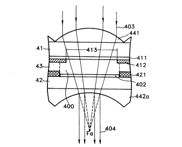
Fig.5 illustrates a pixel area of a liquid crystal
display panel based upon Fig.3. Referring to Fig.5, first and
second substrates 41 and 42 are arranged to be spaced apart by
a predetermined distance. Liquid crystal 43 is filled between
the first and second substrates 41 and 42. A conventional
driving means for driving the liquid crystal 43 is provided on
¦ the internal surfaces of first and second substrates 41 and
42. A pair of TFTs 421 serving as the switching element of the
driving means are placed on the internal surface of the second
substrate 42 with a predetermined distance from each other,
and a pixel electrode 402 for driving the liquid crystal is
located between TFTs 421. Transparent common electrode 411 is
3 formed on the overall internal surface of first substrate 41
for driving the liquid crystal 43 in conjunction with pixel
electrode 402. A pair of black matrices 412 for defining a
light-transmitting region 413 corresponding to each pixel
electrode 402 is provided on common electrode 411. A first
microlens 441 (a convex-plano lens) corresponding to each
light-transmitting region 413 for convergently refracting
incident light rays 403 onto the pixel area of liquid crystal
43 via light-transmitting region 413 is attached on the
external surface of the first substrate 41. A corresponding
'
. :
212~098
~lano-concave second microlens 442a (a plano-convex lens) for
divergently refracting output light rays 404 and rendering
them parallel with the optical axis is provided on the
external surface (at the bottom in the drawing) of second
substrate 42.
Here, second microlens 442a is located between first
microlens 441 and principal focus Fa of first microlens 441.
First and second microlenses 441 and 442a may be attached
directly on the respective external surfaces of first and
second substrates 41 and 42, or may be spaced apart from the
first and second substrates 41 and 42 by a predetermined
distance.
In the liquid crystal display panel of the present
invention, incident parallel light rays 403 are convergently
refracted while passing through first microlens 441, and then
,j are made incident on pixel 400. Output light rays 404 passing
'.i
`i through pixel 400 are divergently refracted by second
microlens 442a and rendered parallel to the optical axis. Such
~ a compensation of the output light rays realizes a fine image.
f~ 20 Since first microlens 441 converges all of the incident light
~ rays and focuses the converged light rays on the pixel, most
i~ of the light is made to be incident on the pixel 400, not
reaching the black matrix 412. This prevents light blockage by
. the black matrix 412 and therefore enhances the pixel
:~, 25 luminance. The incident light rays converged by the first
~` microlens 441 and passing through the pixel 400 are refracted
,~ and diverged while passing through the second microlens 442a
to become parallel with the optical axis. Here, the second
. ,
,, .
,
212~098
microlens 442a functions to render parallel the incident light
rays converged by the first microlens 441. With the second
microlens 442a, the linearity of the output light rays is
enhanced to thereby realize a sharp image.
Fig.6 illustrates another embodiment of the liquid
crystal display panel of the present invention. In this liquid
crystal display panel, a second microlens 442b is a plano-
$ convex lens so as to refractively converge the light rays
passing out of the pixel area 400. Since second microlens 442b
is located outside of the focal length of first microlens 441,
second microlens 442b reconverges the light rays converged by
first microlens 441 and then diverged after passing through
focus Fb, so as to render parallel the diverged light rays.
The second embodiment yields the same effect as that of the
first embodiment by outputting the light rays in parallel.
;~ As another method for realizing such light ray
convergence and parallel light rays, a light converging means
may be constructed to converge incident light rays by stacking
material in which the index of refraction is gradually lowered
from the center to the periphery, on portions of the first
~ substrate corresponding to light transmitting regions 413. In
`' portions of the second substrate corresponding to the light
emitting regions, a light compensating means serving as the
second microlens may be provided to have a converging or
diverging effect by stacking material in which the index of
refraction is gradually lowered or increased from the center
to the periphery.
Further, as another embodiment, the portions
\
. ~
. :: : . , :
212~098
corresponding to the light transmitting regions and light
emitting regions of the first and second substrates may be
processed in a predetermined pattern so as to obtain a
microlens array having a desired form.
Fig.7 shows a schematic configuration of a liquid crystal
projector of the present invention.
Referring to Fig.7, the liquid crystal projector of the
present invention having a similar structure to the
conventional one, includes a parabolic reflection mirror 120
for reflecting light emitted from a light source 100, a liquid
' crystal display panel 40 disposed along the proceeding path of
the light reflected by the reflection mirror, and driven by a
driving circuit 78, polarizing plates 140 and 150 located in
~ front of and behind liquid crystal display panel 40 for
r 15 controlling the polarization of light, and a projection lens
system 160 disposed along the proceeding path of the light
having passed through liquid crystal 40 for projecting an
enlarged projection image onto a screen 170.
As a feature of the present invention, first and second
microlens sheets 440 and 442 are provided, each having
respective microlenses 441 or 442a (or 442b) which correspond
to one another. The first microlens sheet 440 is a light
converging means which converges, in units of pixels, incident
light rays 79 emitted from light source 100, reflected by the
reflection mirror 120 and having only a specific polarized
component filtered by polarizing plate 140, and then passes
the converged light rays to liquid crystal display panel 40.
The second microlens sheet 442 is a light compensating means
11 '
.
: : : .
212~098
which compensates for the light passing through liquid crystal
display panel 40 in units of pixels so as to form parallel
output light rays 80.
Liquid crystal display panel 40 operates in accordance
; 5 with an image signal from driving circuit 78 so as to transmit
or block incident light 79 in units of pixels. Microlenses
441, 442a and 442b of the first and second microlens sheets
440 and 442 are the same as those of the liquid crystal
display panel of the present invention. If the output light
:~ 10 rays passing through the liquid crystal are in a state of
divergence, the second microlens 442a compensates for the
.. diverged output light rays by its converging effect so as to
render parallel the output light rays 80. If the output light
~,. rays passing through the liquid crystal display panel are in a
state of convergence, the second microlens 442b compensates
~ for the converged output light rays by its diverging effect so
` as to render parallel the output light rays 80. The output
light rays compensated as above while passing through the
second microlens sheet 442 reach screen 170 via projection
lens system 160 and therefore form an enlarged image on the
screen 170.
In the liquid crystal projector, since the light to be
passed through the liquid crystal display panel is converged
: by the first microlens sheet serving as the light converging
25 means and having the first microlens array, the effective
pixel aperture ratio of the liquid crystal display panel is
enhanced. Further, since the light rays converged by the light
converging means are converted into parallel light rays by the
12
:. . :: :
, : : ~ ~ : : , :
~250g8
second microlens sheet serving as the light compensating means
and having the second microlens array, the divergence angle of
the light rays passing through the projection lens system is
greatly reduced compared with that of the conventional liquid
crystal projector. Accordingly, an image obtained on the
screen by projecting the output light rays passing through the
projection lens system at a reduced divergence angle becomes
more clear than that from the conventional projector. In
addition, since the diameter of the projection lens system can
be reduced compared with that of the conventional one, it is
feasible to miniaturize the projection lens system and to
thereby decrease the production cost of the whole projector.
13
.: : ~ ' '.' ' , :
- .