Note: Descriptions are shown in the official language in which they were submitted.
CA 02125302 1997-09-08
MULTIPLE DIODE LASER EMPLOYING MATING SUBSTRATES
This invention relates generally to a raster output scanning apparatus
for a printing machine, and more particularly to multibeam laser produced
from a plurality of laser diodes.
CROSS REFERENCE
The following related documents are hereby referred to for their
teachings:
1 o U.S. Patent No. 5,371,526 to James Appel et al., entitled "A Raster
Output Scanner for a Multi-Station Xerographic Printing System Having
Laser Diodes Arranged In a Line Parallel to the Fast Scan Direction";
U.S. Patent No. 5,343,224 to Thomas L. Paoli, entitled "Diode Laser
Multiple Output Scanning System";
U.S. Patent No. 5,276,463 to John R. Andrews, entitled "Raster Output
Scanning Arrangement for a Printing Machine"; and
U.S. Patent No. 5,432,535 to John R. Andrews et al., entitled "Method
and Apparatus for Fabrication of Multibeam Lasers".
2 o BACKGROUND AND SUMMARY OF THE INVENTION
The present invention is directed to flying spot scanners (commonly
referred to as raster output scanners (ROSs)) which typically have a
reflective
multifaceted polygon mirror that is rotated about its central axis to
repeatedly
sweep one or more intensity modulated beams of light across a
2 5 photosensitive recording medium in a line (fast) scanning direction. While
the beams sweep across the photosensitive recording medium, it is advanced
in an orthogonal, or "process", direction, commonly , referred to as the slow-
scan direction, such that the beams scan the recording medium in accordance
with a raster scanning pattern. Digital printing is performed by serially
3 0 modulating the intensity of each of the beams n accordance with a binary
sample stream, whereby the recording
-1-
212532
medium is exposed to the image represented by the samples as it is being
scanned.
Printers that sweep several beams simultaneously are referred to
as multibeam or multispot printers. Moreover, dual or multispot lasers are
considered to be an enabling technology for high speed printers operating
at resolutions of about 600 spots per inch (spi) while producing output at
greater than 80 pages per minute (ppm). Monolithic laser arrays, while
providing the multispot capability, have typically been strongly sensitive to
thermal crosstalk when used in closely spaced lasers having interbeam
spacings of less than 250 Vim, and are not easily adapted to provide multiple
wavelength and/or multiple polarity laser beams.
The following disclosures relate to both ROS printing devices
and multibeam laser diodes which may be relevant:
US-A-5,060,237
Patentee: Peterson
Issued: Oct. 22, 1992
US-A-4,901,325
Patentee: Kato et al.
Issued : Feb. 13, 1990
US-A-4,892,371
Patentee: Yamada et al.
Issued: Jan.9, 1990
U S-A-4,884,857
Patentee: Prakash et al.
Issued: Dec. 5, 1989
_2_
2125302
US-A-4,474,422
Patentee: Kitamura
Issued: Oct. 2, 1984
US-A-4,404,571
Patentee: Kitamura
Issued: Sep. 13, 1983
US-A-4,393,387
Patentee: Kitamura
Issued: Jul. 12, 1983
US-A-4,293,826
Patentee: Scifres et al.
Issued: Oct. 6, 1981
The relevant portions of the foregoing disclosures may be briefly
summarized as follows:
US-A-5,060,237 discloses a laser diode array including a plurality
of laser diode bodies affixed to a surface of a substrate. Each of the laser
bodies includes a semiconductor junction therein which is capable of
generating light in response to a voltage potential. An end surface of the
body is angled at a forty-five degree angle so as to reflect the light
generated by the diode in a direction which is orthogonal to the surface of
the substrate.
US-A-4,901,325 teaches a semiconductor laser device used in an
optical disk device which utilizes a pair of semiconductor laser chips and a
fixing device for fixing the laser chips so that the electrode surfaces are
approximately parallel and opposite to each other. The fixing device
comprises either a smgie-piece, U-shaped block or, alternatively, a pair of
blocks, upon which the photodiodes are ultimately mounted.
US-A-4,892,371 describes a semiconductor laser array light
source and scanner wnerein the laser light source emits one or more pairs
-3-
2125302
of light beams. The light beams are collimated by a collimating lens and are
subsequently directed along separate paths. Additional optical means are
used to transmit or reflect certain of the light beams to one or more
incident surfaces of the optical means so as to align the beams by
controlling the angle of incidence and beam separation at a photosensitive
surface.
US-A-4,884,857 teaches a multiple spot printer which employs a
laser system having multiple semiconductor lasers, an aperture plate, and
an optical system as shown in Figures 4 and 5. Control of the spot locations
at the surface of the photoconductor is achieved in two planes, first, using
an aperture plate in the process plane, and second, using a single aperture
plate in the scan plane.
US-A-4,474,422 discloses an optical scanning apparatus having a
light source consisting of an array of aligned light sources. The beams from
the light sources are collimated and deflected to sweep across a single
photoreceptor. The beams are also displaced from each other in the cross-
scan direction so that multiple lines can be scanned simultaneously across
the photoreceptor. An object of US-A-4,474,422 is to reduce variations in
pitch by closely spacing individual lasers within the laser array in a compact
structure.
US-A-4,404,571 describes a multibeam recording apparatus
comprising a scanner for scanning a recording medium with a plurality of
light beams and a beam detector. The scanner employs a laser array light
source having a plural number of semiconductor lasers arranged in a row.
The beam detector utilizes a screen plate with a detection aperture which is
smaller than the inter-beam spacing to individually detect each of the
plural beams.
US-A-4,393,387 teaches a beam recording apparatus including a
semiconductor array laser light source having a plurality of light beam
emitting points, a condensing optical system, an image rotator, and a
rotatable polygon mirror for deflecting the light beams to the surface of a
photosensitive drum. High density recording is enabled by controlling the
-4-
CA 02125302 2000-04-03
angle of incidence, and therefore the interbeam spacing, of the outermost
beams at the
surface of the photosensitive drum.
US-A-4,293,826 discloses a semiconductor injection laser having an optical
feedback control incorporated within the same semiconductor chip.
Stabilization of the
laser output is accomplished by monitoring a portion of the light output with
an optical
detector, which then drives a feedback circuit to control the laser current.
The patent
further describes a hybrid semiconductor laser/detector arrangement which
implements
an array of laser/detector pairs on a single semiconductor substrate.
1 o In accordance with the present invention, there is provided a multiple
spot laser
assembly, comprising: a plurality of laser diodes, wherein each of said laser
diodes
emits at least one light beam; a plurality of mounts, each of said plurality
of mounts
including a support surface with a laser diode affixed to the support surface,
wherein
said mounts are movable with respect to one another and wherein each of said
plurality of mounts is identical; means for aligning a first one of said
plurality of
mounts with an adjacent one of said plurality of mounts including means,
located on
each of said mounts, for interlocking said mounts by contact between a
plurality of
mating surfaces on said mounts, wherein at least two adjacent surfaces of the
plurality
of mating surfaces on said mounts form an obtuse angle therebetween and where
the
2 0 interlocking means limits relative motion between adjacent mounts in at
least two
directions perpendicular to the light beams emitted from said laser diodes,
thereby
aligning said laser diodes affixed to each of the plurality of mounts while
maintaining
the support surface of each of said mounts and said laser diodes affixed to
the support
surface in a spaced apart relationship to avoid thermal crosstalk between the
laser
2 5 diodes; and means for joining said plurality of mounts in a permanent
fashion.
In accordance with another aspect of the present invention, there is provided
a
raster output scanning apparatus for producing a latent electrostatic image by
selectively exposing an electrostatically charged surface of a photoresponsive
member, comprising: a multiple spot laser, including: a first laser diode for
producing
-5-
CA 02125302 2000-04-03
a first beam, a second laser diode for producing a second beam, first mounting
means
for supporting the first laser diode such that said first laser diode is
mounted on said
first mounting means, second mounting means for supporting the second laser
diode
such that said second laser diode is mounted on said second mounting means,
said
first mounting means and said second mounting means being independently
movable
with respect to one another, each of said first mounting means and said second
mounting means having a support surface to which a laser diode is affixed and
wherein said first mounting means and said second mounting means are
identical, and
means for aligning said first mounting means with respect to said second
mounting
means, said aligning means including a plurality of mating surfaces located on
each of
said first mounting means and said second mounting means, wherein at least two
adjacent surfaces of the plurality of mating surfaces located on each of said
first
mounting means and said second mounting means form an obtuse angle
therebetween
and where the plurality of mating surfaces provides interlocking alignment
between
said first mounting means and said second mounting means to limit relative
movement therebetween in at least two directions in a plane perpendicular to
the first
beam and the second beam respectively emitted from said first diode and said
second
diode when said first mounting means and said second mounting means are placed
in
contact, said first mounting means and said second mounting means further
2 0 maintaining the support surface for the first laser diode and the support
surface for the
second laser diode in a spaced apart relationship when said first mounting
means and
said second mounting means are placed in contact; means for joining the first
mounting means and the second mounting means in a permanent fashion; means for
deflecting the first beam and the second beam of said multiple spot laser into
an
2 5 optical path; and means for directing the first beam and the second beam
of said
multiple spot laser toward the electrostatically charged surface of the
photoresponsive
member to expose regions thereof in order to generate a latent electrostatic
image
thereon.
- Sa -
CA 02125302 2000-04-03
BRIEF DESCRIPTION OF THE DRAWINGS
Figure 1 shows a single-pass ROS color printing system with a housing
incorporating a dual beam raster output scanning system;
s Figure 2 is a perspective view illustrating the optical elements
incorporated
within another dual beam ROS, namely a light source,
15
25
-Sb -
CA 02125302 1997-09-08
polarization control system, beam forming optics system, deflector and
corrective optical system;
Figure 3 is a perspective view of the light source of Figure 2
illustrating one embodiment of the present invention;
Figure 4 is another perspective view of the light source illustrating an
alternative embodiment of the present invention, wherein a multibeam laser
configuration is shown; and
Figure 5 is yet another perspective view of a multibeam embodiment
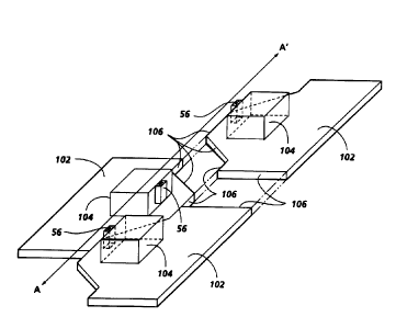
1 o for the light source of Figure 2 in accordance with the present invention.
The present invention will be described in connection with a preferred
embodiment, however, it will be understood that there is no intent to limit
the invention to the embodiments described. On the contrary, the intent is to
cover all alternatives, modifications, and equivalents as may be included
within the spirit and scope of the invention as defined by the appended
claims. For example, the present invention may very well be employed to
achieve a semiconductor laser for use in an optical disk device similar to
that
described by Kato et al. in US-A-4,901,325.
2 o DESCRIPTION OF THE PREFERRED EMBODIMENT
For a general understanding of the present invention, reference is
made to the drawings. In the drawings, like reference numerals have been
used throughout to designate identical elements. Figure 1 shows a single-
pass ROS color printing system 2, which includes a ROS housing 4. As
2 5 depicted, system 2 produces two separate output scanning beams, 10 and 12,
although it is understood that a multibeam system, having greater than two
beams, would have a similar configuration. System 2 further includes a
photoreceptor belt 14, driven in the process direction, indicated by the arrow
15. The length of belt 14 is designed to accept an integral number of spaced
3 0 image areas h -In represented by dashed line rectangles in Figure 1.
Upstream of each exposure station are charge devices (not shown) which
place a predetermined electrical charge on the surface of belt 14. As the belt
moves in the indicated direction, each image area is scanned by a
3 5 -6-
CA 02125302 1997-09-08
succession of scan lines to provide an image exposure pattern in response to
image data signals which are input to the respective ROSS. The exposure
pattern begins when the leading edge of image area 23 reaches a transverse
start-of-scan line represented by dashed arrow 20. The exposure pattern is
formed of a plurality of closely spaced transverse scan lines 24 shown with
exaggerated longitudinal spacing on image area I2. Downstream from each
exposure station, development systems develop a latent image of the last
exposure without disturbing previously developed images. A fully
developed color image is then transferred by means not shown to an output
sheet. System 2 may be a two color (highlight plus black) printer, although
the plural beams emitted from ROS housing 4 may similarly be used to
expose a single image area, thereby providing increased writing speed
and/or increased writing density to a single image area, In, as described in
the previously incorporated patents, for example, US-A-4,474,422 to
Kitamura. Further details of the operation of xerographic stations in a
multiple exposure, single-pass system are disclosed in US-A- 4,660,059 to
O'Brien and US-A-4,791,452 to Kasai et al.
Further depicted in Figure 1 are pairs of beam steering sensors 26 and
2 0 28, which used to sense the location of the scan lines as they traverse
the
surface of the photoreceptor. The sensor heads may also be used as start-of-
scan (SOS) sensors, to determine the time at which the laser beam traverses a
specific point, the occurrence of this event being used to synchronize the
start-of-scan locations for each of the individual image frames, h - In,
thereby
2 5 registering the frames in the fast-scan, or Y, direction.
Referring to Figure 2, the illustrated ROS system employs a light
generating device 34, which, as shown in the following figures can comprise
a plurality of relatively closely spaced laser diodes, 56. Typically, the
laser
diodes are separated from one another by a distance which is preferably less
3 0 than or equal to 250 ~,m. In one example, the light generating device
emits
two laser beams 48 and 50, which may have different wavelengths, for
example, 650 nm and 685 nm, respectively. As is
CA 02125302 1997-09-08
apparent from the cross referenced patents, specifically, U.S. Patent No.
5,276,463 by John R. Andrews, the ROS arrangement of the present invention
can be practiced with more than two laser beams, while the respective
wavelengths and/or respective polarizations of the employed beams can be
altered significantly without affecting the concept upon which the present
invention is based. For purposes of clarity, in various drawings of the
present application, only the chief rays of the beams 48 and 50 are shown.
Light generating device 34 effectively provides a substantially common
spatial origin for each beam. Each beam is independently modulated so that
it exposes the photoreceptor in accordance with a respective digitized image.
Still referring to Figure 2, the laser beams from device 34 are input to a
segmented waveplate 36, and then optics system 38, which preferably
includes a collimator lens to direct the beams onto an optical path such that
they illuminate the deflector 42, which, in one example, comprises a rotating
polygon mirror having a plurality of facets 44. As the polygon mirror rotates,
the facets cause the reflected beams to deflect repeatedly for input to the
correction optical system 46, which focuses the beams and corrects for errors
such as polygon angle error and wobble prior to transmitting the beams to
the surface of the photoreceptor.
2 0 Turning now to Figure 3, where the dual spot embodiment of light
generating device 34 is shown, the dual spot laser assembly illustrated is
comprised of two identical halves. The halves, or mounts 60a,b are separable
pieces which interlock to provide precise alignment of laser diodes 56 affixed
thereto. The laser diodes may be any commonly available single-beam solid
2 5 state laser diode, for example, the Toshiba 9211 VLD. Mounts 60a,b are
comprised of a base plate 62 and a heat sink 64. While shown as two distinct
elements, where the heat sink is attached to a surface of the base plate, it
is
conceivable that the base and heat sink be machined from a single billet to
produce the illustrated structure. Furthermore, heat sink 64 has a flat
surface,
3 0 orthogonal to the plane of the base plate, upon which the laser diode 56
is
permanently affixed. The heat sink and base are preferably formed from a
thermally conductive material,
_g_
212302
such as copper, thereby providing heat dissipation and and an electrical
path via contact with the junction side of the laser diode. Instead of the
commonly known circular base used in conventional laser light sources, the
present embodiment utili2es two semicircular base plates having alignment
features for aligning the two halves during assembly. Also included in
mounts 60a,b, are sealed through-plate conductors, 68, suitable for
carrying electrical signals through the base plate. For example, conductors
68a supply power to laser diode 56, while conductors 68b provide electrical
power to, and return electrical signals from, photodetector 66. All
conductors are wire bonded to contacts on the laser diodes and the
photodetectors, thereby providing electrically conductive paths for
connection to external laser driving and feedback circuitry (not shown).
Following assembly, the two mounts 60a,b would be
permanently joined to one another, possibly using a welded or low
temperature Indium compression bond or even an epoxy bond.
Alternatively, a low temperature Indium alloy solder may be used to
connect the base plates, while a higher temperature Indium-Lead solder
may be used to affix the laser diode to the heat sink. Soldering the two
mounts to produce a metal seal therebetween would enable the further
addition of an organic-free hermetic seal of the laser light generating
device when a windowed cap is put in place, as is commonly practiced in the
laser industry, to complete packaging. To further prevent potential contact
and shorting of the conductors, 68a, which supply power to the two lasers,
during assembly of the halves a small spacer could be placed between the
two lasers, and then removed prior to placing the windowed cap over the
entire assembly. Since the individual lasers are on the order of 70 ~m thick,
measured along the A-A' line, the two wirebonds are intended to be made
to fit into a separation between the top laser surfaces of 110 um resulting
in a laser spacing of 250 Vim. As further depicted in the figure,
complimentary cone-shaped projections and depressions, 70 and 72,
respectively, are used as the alignment features for the two semicircular
mounts. Once aligned and assembled, laser diodes 56 produce two parallel
_g_
CA 02125302 1997-09-08
light beams, indicated by reference numerals 48 and 50, the centers of which
are aligned along line A-A'.
Turning now to Figure 4, which illustrates an alternative
embodiment of the present invention, base plates 62, while remaining
semicircular in shape, both contain a complimentary step, 80, along the
mating surfaces thereof. In this embodiment, the mounts, 82a,b, are
assembled in the manner previously described with the interlocking feature
being the step. The assembly process for the depicted embodiment would
also require a planar surface upon which the backsides of mounts 82a,b
would rest during assembly. The planar assembly surface would facilitate
the accurate alignment of the mounts so that the emitting faces the four laser
diodes, 56, are maintained in or near a common plane as well.
Also depicted in Figure 4 is a quad-beam diode arrangement, wherein
four laser diodes are assembled along a line A-A'. In the quadbeam
embodiment, each laser diode is mounted junction side facing a chip carrier,
86, where the chip carrier is bonded to heat sink 64. As described in detail
in
copending U.S. Patent No. 5,432,535 by John R. Andrews et al., entitled
"Method and Apparatus for Fabrication of Dual Lasers", the chip carrier may
2 0 be formed from a material suitable for sufficiently reducing thermal cross-
talk between the pair of laser diodes affixed thereto. As in the previously
described embodiment, the split-base design is commonly used for both of
the mount halves, thereby enabling easy access to the laser diodes during
manufacture, yet providing a closely spaced laser diode array when
2 5 assembled.
Now considering the multispot embodiment depicted in Figure 5, the
previously described base plate,102 and heat sink, 104 elements are used
once again, but are now arranged in a linear fashion, rather than the
previously described two-part, semicircular embodiments. More specifically,
3 0 the planar base plates, 102, each have one or more mating surfaces 106,
which
are designed to positively mate with adjoining surfaces of adjacent base
plates. While mating surfaces 106 are generally depicted as being orthogonal
to the planar surface of the base plate, it would be
3 5 - 10-
212302
possible to produce the base plates with all of the mating surfaces
consisting of complimentarily angled surfaces (not shown) to further
improve the interlocking nature of the plates. Whatever mating surface
configuration is chosen, angled or orthogonal, the alignment of the laser
diodes along a single line is achieved as a result of the interlocking nature
of the base plates, and in response to externally applied forces which tend
to push the base plates together. Once held in an aligned relationship, the
base plates would be permanently connected to one another using the
aforedescribed soldering or equivalent joining operations. Figure 5
illustrates the potential for a lengthy multispot array, where laser diodes 56
are maintained in an aligned relationship, along line A-A', by the
configuration, or shape, of the base plates. Moreover, all the base plates
are again of a single, common design, thereby eliminating the need for
more than one type of mount to complete the assembly. While not
specifically illustrated, it is believed to be apparent, from the embodiment
illustrated in Figure 5 that the present invention may also be used to
produce two-dimensional arrays of laser diodes using the previously
described alignment features. Such an array would comprise a plurality of
laser diodes aligned along at least two lines parallel to the A-A' line
illustrated in Figure 5.
In recapitulation, the present invention is a multispot laser light
source assembled from a plurality of individual laser diodes, wherein tvvo or
more mounting means, each containing at least one laser diode on a
surface thereof, are aligned with one another to produce the multiple spot
laser source. The present invention is further characterized by
complimentary alignment features, found on the mounting means so as to
result in the positive alignment of the mounts and the laser diodes affixed
thereto.
It is, therefore, apparent that there has been provided, in
accordance with the present invention, a method and apparatus for reliably
and efficiently producing a multispot laser device from a plurality of
distinct mounting means, wherein the mounting means are all of a
common design. While this invention has been described in conjunction
-11-
2125302
with preferred embodiments thereof, it is evident that many alternatives,
modifications, and variations will be apparent to those skilled in the art.
Accordingly, it is intended to embrace all such alternatives, modifications
and variations that fall within the spirit and broad scope of the appended
claims.
-12-