Note: Descriptions are shown in the official language in which they were submitted.
2125~06
.~
PATENT APPLICATION
Attorney Docket No. D/92481
INK JET PRINTHEAD HAVING COMPENSATION FOR TOPOGRAPHICAL
FORMATIONS DEVELOPED DURING FA8RICATION
BACKGROUND OF TH E INVENTION
The present invention relates to a thermal ink jet printhead and
method of manufacture therefore, and more particularly to an improved
thermal ink jet printhead having minimized standoff between two bonded
parts by compensating for topographic formations developed in an
insulating layer during fabrication.
In existing thermal ink jet printing systems, an ink jet printhead
expels ink droplets on demand by the selective application of a current
pulse to a thermal energy generator, usually a resistor, located in capillary-
filled, parallel ink channels a predetermined distance upstream from the
channel nozzles or orifices. U.S. Re. 32,572 to Hawkins et al exemplifies
such a thermal ink jet printhead and several fabr,icating processes therefor.
Each printhead is composed of two parts aligned and bonded together.
One part is a substantially flat substrate which contains on the surface
thereof a linear array of heating elements and addressing elements (heater
plate), and the second part is a substrate having at least one recess
anisotropically etched therein to serve as an ink supply manifold when the
two parts are bonded together (channel plate). A linear array of parallel
grooves are also formed in the second part, so that one end of the grooves
communicate with the manifold recess and the other ends are open for use
as ink droplet expelling nozzles. Many printheads can be made
simultaneously by producing a plurality of sets of heating element arrays
with their addressing elements on a silicon wafer and by placing alignment
marks thereon at predetermined locations. A corresponding plurality of
sets of channel grooves and associated manifolds are produced in a second
silicon wafer. In one embodiment, alignment openings are etched in the
second silicon wafer at predetermined locations. The two wafers are
2125~0S
.,~
aligned via the alignment openings and alignment marks, then bonded
together and diced into many separate printheads.
Improvements to such two part thermal ink jet printheads
include U.S. Patent 4,638,337 to Torpey et al that discloses an improved
printhead similar to that of Hawkins et al, but has each of its heating
elements located in a recess (termed heater pit). The recess walls
containing the heating elements prevent lateral mo~/ement of the bubbles
through the nozzle and therefore the sudden release of vaporized ink to
the atmosphere, known as blow-out, which causes ingestion of air and
interrupts the printhead operation whenever this event occurs. In this
patent, a thick film organic structure such as polyimide, Riston~ or Vacrelo is
interposed between the heater plate and the channel plate. The purpose
of this layer is to provide the recesses for the heating elements, so that the
bubbles which are formed on the heating elements are laterally
constrained, thus enabling an increase in the droplet velocity without the
occurrence of vapor blow-out and concomitant air ingestion. U.S. Patent
No. 4,774,530 to Hawkins further refines the two part printhead by
disclosing an improvement over the patent to Torpey et al. Further recesses
(termed bypass pits) are patterned in the thick film layer to provide a flow
path for the ink from the manifold to the channels by enabling the ink to
flow around the closed ends of the channels, thereby eliminating the
fabrication steps required to open the groove closed ends to the manifold
recess. The heater plates, having the aforementioned improvements of
heater pits and bypass pits formed in the thick film organic structure
covering the heater plate surface, are aligned with the channel plate, so
that each channel groove has a recessed heating element therein.
Thorough bonding between heater and channel plates is
paramount to maintaining the efficiency, consistency, and reliability of an
ink jet printhead. U.S. 4,678,529 to Drake et al. discloses a method of
bonding ink jet printhead components together by spin coating or spraying
a relatively thin, uniform layer of adhesive on a flexible substrate and then
manually placing the flexible substrate surface with the adhesive layer
against a printhead component surface. A uniform pressure and
-
temperature is applied to ensure adhesive contact with
all coplanar surface portions and then the flexible
substrate peeled away, leaving a uniformly thin coating
on the surface to be bonded. A roller or vacuum
lamination may be applied to the flexible substrate to
insure contact on all of the lands or coplanar surfaces
of the printhead part. Unfortunately, this labor
intensive method permits adhesive layer thickness
variation between a plurality of identical parts, so that
ink flow characteristics varies from printhead to
printhead. Accordingly, a more mechanized process to
place the adhesive coating on the disk with the channel
wafer was required to minimize operator involvement and
consequent variation in parameters which introduced
thickness variations in the amount of adhesive layer
transferred to the channel wafers, especially in the
thickness variations from wafer-to-wafer. This process
is described in U. S. Patent No. 5,336,319 to Narang et
al, issued August 9, 1994. The process includes the step
of applying a uniform thick layer of adhesive to one
surface of a plurality of planar substrates, one
substrate at a time, by a method and apparatus which
controls both the adhesive layer thickness on each
substrate surface and the thickness variations from
substrate-to-substrate. As a result, consistent, repeat-
able, uniformly thick adhesive layers may be applied to
each of a plurality of substrates, and the applied layers
meet the same tolerance for thickness variation.
Although advances have improved the adhesive layer
thickness which bonds the ink jet printhead heater and
channel plates, insufficient adhesion between bonded
heater and channel plates continues to cause a host of
problems affecting channel firing consistency such as
different drop sizes between adjacent channels. Since
-3-
~t~
.
5 3 ~ ~ -
'._
increased adhesive layer thickness is not a practical
solution because it tends to spread or wick into the
channel, the inter-channel gaps between bonded heater and
channel plates must be minimized in order to insure
consistent printhead firing characteristics. As taught
by the above identified U. S. patents, two wafers are
bonded together after alignment for subsequent dicing
into individual printheads. Each printhead part is
formed individually on two separate substrates or wafers,
where one contains heating elements and the other ink
channels or
,;~
~i
.
2125306
passageways. The wafer containing the ink channels is silicon, and the
channels are formed by an anisotropic etching process. The anisotropic or
orientation dependent etching has been shown to be a high yielding
process that produces very planar and highly precise channel plates. The
other wafer containing the heating elements as well as heater addressing
logic is covered by a thick film organic structure in which heater and bypass
pits are formed using photolithography. The thick film organic structure
used to protect silicon substrates is often formed with polyimide, which is
also used as an interconnect material and insulator. Because of its
beneficial property of being impervious to water, it is commonly considered
a standard material for protecting circuitry on silicon substrates. However,
one drawback with the polyimide material is its tendency to form
unwanted topographical formations, such as raised edges or lips (1-3
microns high) at any photoimaged edge. When bonding both heater and
channel plates together, a standoff between the two plates is caused by the
raised edges, which reduces the adhesiveness of the bond between the two
plates and which cause the formation of inter-channel gaps.
Polyimide topography, such as raised edges, are undesirable by-
products resulting from photoimaged heater and bypass pits on heater
plates. The raised edges, are polyimide topographical features that critically
interfere with the proximity at which heater and channel plates are bonded
together. Raised edges, however, are not the only topographical
formation created from photoimaged polyimide. Other topographical
formations, such as wall sags or dips, compound the negative effects of
raised edges by adding to the standoff between the bonded heater and
channel plates. Wall dips are slumps in the polyimide walls between
polyimide photoimaged pits. The polyimide sandwiched between the two
wafers or plates can form more than 2 microns of topographical variation,
which does not allow the bonding adhesive, approximately 2 microns or
less thick, to bridge or fill in the formation of inter-channel gaps. These
inter-channel gaps can allow crosstalk between channels when drops are
being ejected. As the patent '529 to Drake et al teaches, care must be taken
when applying adhesive in bonding the channel and heater plates so as to
3 ~ ~ '
'~ insure all fluid surfaces in contact with ink are free of
adhesive in order that they are not obstructed during
operation. There exists, therefore, a need to improve
the adhesion between the bonded heater and channel plates
in order to minimize inter-channel gaps by reducing the
standoff between the butted plates without increasing the
amount of adhesion or epoxy used in bonding them.
SUMMARY OF THE lNvh~lION
It is an object of an aspect of the invention to
minimize the standoff between bonded heater and channel
plates of a printhead, with minimal impact to the
existing fabrication sequence of the printhead.
It is an object of an aspect of the invention to
provide a more reliable printhead that minimizes the
effects of topographic formations in the thick film
insulating layer that induce inter-channel gaps which
degrade the reliability and performance of the printhead.
To achieve the foregoing and other objects, and to
overcome the shortcomings discussed above, improvements
to an ink jet printhead assembly are provided that
eliminate the standoff between plates of printheads of
the type formed by the alignment and bonding of an
anistrophically etched silicon wafer ch~nnel plate,
containing an array of channel grooves, to a patterned
thick film insulating layer formed on a surface of a
silicon wafer heater plate, containing an array of
heating and addressing elements. The heating elements
are disposed in pits formed in the thick film insulating
layer. The plate standoff is caused by topographic
formations introduced while forming some of the
photoimaged recesses in the thick film insulating layer.
The present invention introduces elements into the
fabrication sequence of the printhead that compensate for
the topographic formations.
, ,~
..... "
3 ~ ~ -
",
In an array of pits formed using a photopatternable
insulating layer, such as polyimide, distinct formations
exist in certain locations which produce the standoff
between the heater and channel plates of the ink jet
printhead. It has been determined that a polyimide
topographic formation, such as, for example, a pronounced
raised edge or lip is formed only at the outside edge of
the last pit in an array of pits because of the increased
mass of polyimide between sets of pits. In the preferred
embodiment, an additional non-functional clearance
channel is formed on opposite sides of the array of
channels, along with a corresponding additional, offset
pit to position the raised edge formation into the
clearance channel. The improved printhead eliminates
standoff between the chAnnel and heater plate caused by
the raised edge thereby substantially eliminating the
inter-channel gaps which cause inconsistent adhesive
bonding and degrade printhead performance. The printhead
fabrication is accordingly modified to include an edge
straddling clearance chAnnel that prevents the standoff
created by the raised edge.
A corresponding additional offset pit optionally
positioned the raised edge of the straddling clearance
channel further from the functional channels.
Another aspect of this invention is as follows:
An improved ink jet printhead of the type having a
silicon upper substrate which has one surface that is
anisotropically etched to form a set of parallel grooves
and an ink supply manifold therein, the set of parallel
grooves being used as a linear array of ink channels for
providing communication between the ink supply manifold
and a set of droplet ejecting nozzles in said printhead,
and further having a lower substrate which has one
surface that has an array of heating elements and
,'1
.~m
addressing electrodes formed thereon, the upper and lower
substrates being aligned, mated, and bonded together to
form the printhead with a thick film insulating layer
sandwiched therebetween, the thick film insulating layer
having been deposited on the surface of the lower
substrate having the array of heating elements and
addressing electrodes thereon and patterned to form
recesses therethrough prior to alignment, mating and
lo bonding of the upper and lower substrates, the recesses
forming arrays of heater pits and channel bypass recesses
to correspond in number and to align with the set of
parallel grooves and array of heating elements, so that
each heating element resides in a heater pit and each
groove of said set of parallel grooves has a heating
element in a heater pit therein and has a bypass recess
interconnecting the groove with the ink supply manifold
to provide communication therebetween, the patterning of
the heater pits and bypass recesses in the thick film
insulating layer producing topographic formations, some
of which cause standoff of the upper substrate, wherein
the improvement comprises:
the thick film insulating layer having defined
therein at least one additional nonfunctional heater pit
and one additional nonfunctional bypass recess on
opposite sides of the arrays of heater pits and bypass
recesses, respectively, said additional nonfunctional
heater pits and bypass recesses relocating the
topographical formations in the thick film insulating
layer which would cause standoff of the upper substrate
away from the array of heater pits and bypass recesses to
the additional nonfunctional heater pits and bypass
recesses which have no other function; and
the upper silicon substrate having formed therein at
least one additional, nonfunctional, parallel groove on
-6a-
~, t
opposite sides of the set of parallel grooves, said
additional nonfunctional grooves straddling the
topographical formations formed proximate to said
additional nonfunctional heater pits and bypass recesses
formed in the thick film insulating layer on the lower
substrate which would have caused the upper substrate to
standoff, so that a standoff between the upper and lower
substrates caused by said topographical formations in the
thick film insulating layer is prevented, because the
topographical formations which would cause the standoff
is located in the additional nonfunctional grooves which
have no other function.
A more complete understanding of the present
invention can be obtained by considering the following
detailed description in conjunction with the accompanying
drawings, wherein like index numerals indicate like
parts.
BRIEF DESCRIPTION OF THE DRAWINGS
FIG. 1 is an enlarged isometric view of a printhead
incorporating the present invention.
FIG. 2 is an enlarged cross-sectional view of FIG. 1
as viewed along the line 2-2 thereof.
FIG. 3 is an enlarged cross-sectional view of FIG. 1
as viewed along line 3-3 thereof.
FIG. 4 is an enlarged cross-sectional view of FIG. 2
as viewed along the line 4-4 and shows the outer opposing
non-functional ink jet channels and corresponding non-
functional pits to eliminate the undesired channel and
heater plate separation.
FIG. 5 is an enlarged cross-sectional view of a
typical prior art ink jet printhead similar to FIG. 4 and
showing the standoff between the heater and channel
plates caused by topographical formations developed
during fabrication.
-6b-
J~ is
_ ~12530~
FIG. 6 is an enlarged cross-sectional view similar to FIG. 4,
showing an alternate embodiment of the present invention.
DESCRIPTION OF THE PREFERRED EMBODIMENT
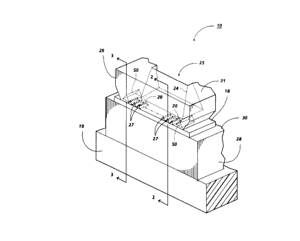
In FIG. 1, an enlarged, schematic isometric view of the printhead
10 incorporating the present invention is depicted, showing the front face
29 thereof containing the array of droplet emitting nozzles 27 and outer,
non-functional channels 50 shown in dashed line. Cross sectional views of
FIG. 1 are taken along view line 2-2 through one active channel 20 and
along view line 3-3 through one non-functional, outer channel 50. FIG. 2
shows how ink flows from the manifold 24 and around the end 21 of the
groove or ink channel 20, as depicted by arrow 23. In FIGS. 1 and 2, the
lower electrically insulating substrate or heating element plate 28 has the
heating elements or resistors 34 and addressing elements 33 produced
monolithically on underglaze insulating layer 39 formed on surface 30
thereof, while the upper substrate or channel plate 31 has parallel grooves
20 which extend in one direction and penetrate through the channel plate
front face 29. On the opposing sides of the arra~ of grooves 20 is a similar
larger groove 50, discussed later, which does not penetrate the front face.
The end of grooves 20 opposite the nozzles terminate at slanted wall 21.
The through recess 24 is used as the ink supply manifold for the capillary
filled ink channels 20 and has an open bottom 25 for use as an ink fill hole.
The surface of the channel plate with the grooves are aligned and bonded
to the heater plate 28, so that a respective one of the plurality of heating
elements 34 is positioned in each channel 20, formed by the grooves and
the lower substrate or heater plate. Ink under a slight negative pressure
enters the manifold formed by the recess 24 and the lower substrate 28
through the fill hole 25 and, by capillary action, fills the channels 20 by
flowing through a plurality of elongated recesses 38 formed in the thick
film insulating layer 18, one for each channel 20. Non-functional channel
50 also has an elongated recess 38, but it does not enable communication
with the ink manifold 24. The ink at each nozzle forms a meniscus, the
combination of negative ink pressure and surface tension
of the meniscus prevents the ink from weeping therefrom.
As disclosed in U. S. Re 32,572 to Hawkins et al.
issued January 5, 1988 and U. S. 4,774,530 to Hawkins
issued September 27, 1988, thermal ink jet die or
printheads 10 are generated in batches by aligning and
adhesively bonding an anisotropically etched channel
wafer (not shown) to a heater wafer (not shown) following
by a dicing step to separate the bonded wafers into
individual printheads 10. Prior to forming the arrays of
heating elements and addressing electrodes on surface 30
of the heater wafer, an underglaze layer 39 is formed
thereon, such as, silicon dioxide or silicon nitride.
After the arrays of heating elements and addressing
electrodes have been formed, a thin film passivation
layer 16 is deposited on the heater wafer surface 30 and
over the heating elements and addressing elements. ~ayer
16 provides an ion barrier which will protect exposed
electrodes from the ink. The thick film insulating layer
18 of photopatternable material, such as, for example,
polyimide, is deposited over the passlvation layer 16 and
is patterned to expose the heating elements, thereby
placing the heating elements in separate pits 26, to
remove the thick film from the electrode terminals 32,
and to remove the thick film layer at locations which
will subsequently provide ink flow bypass recesses 38
between the reservoir 24 and the ink channels 20. The
heating elements are covered by protective layer 17, such
as tantalum, to prevent cavitational damage to the
heating elements caused by the collapsing vapor bubbles.
The printheads are mounted on daughterboards 19 and
electrically connected to electrodes 12 thereon by wire
bonds 14. The daughterboard provides the interface with
the printer controller (not shown) and power supplies
(not shown).
i
FIG. 3 shows a cross-sectional view of the non-
functional channel 50 and shows that this channel
contains a pit 52 without a heating element and an
elon~ated recess 38 that does no provide connection to
the ink manifold 24. Also, shown in FIG. 3 is the lips
or protrusions 40 formed by the patterning process for
the thick film layer 18, which in the preferred
embodiment is polyimide. The unexpected formation of
polyimide lips was
-8a-
,,r
21~30S
.,.
found when the prior art printheads formed by the bonding of channel
plates to heater plates were found to be deficient. Investigation led to the
discovery of various topographic formations that prevented adequate
bonding. When the spacing between the patterned recesses in thick film
polyimide layers was a small dimension, the polyimide material between
the recesses sagged slightly. The pits 26 and bypass recesses 38 shown in
FIG. 2 are closely spaced at 300 per linear inch or more and, therefore, the
material 15 between the pits sunk or sagged slightly. This sagging increases
the severity of the problem of lip formation because of its accumulative
affect on the standoff between the channel and heaters wafers, while the
uniform layer of adhesive deposited on the channel wafer surface having
the plurality of sets of channel grooves 20 and through recesses 24 must be
relatively thin, as disclosed in U.S. 4,678,529 to Drake et al. The thicker the
adhesive layer, the more likely that the adhesive will flow into the channels
and impact printhead performance, so that a relatively thin layer of
adhesive is important. The topographic formation of lips at the edges of
patterned recesses in polyimide and other thick film materials occurs when
the spacing between patterned recesses are relatively large. Thus, the
upstream and downstream ends of the pits and bypass recesses have a
formation of lips 40, because of the relatively large spacing between the set
of heating element arrays on the heater wafer, but do not impact the gap
or standoff between the channel and heater plates because the channel
grooves 20 and through recess 24 straddle these lips. The polyimide lips 40
formed along the outer sides which are parallel to the channels and cause
the channel plate and heater plate to be separated by a gap 42 in prior art
printheads, as shown in FIG. 5. FIG.5is a cross-sectional view through the
heating elements 34 and pits 26 of a prior art printhead and is a view similar
to that of FIG.4, discussed below.
FIG. 4 is an enlarged cross sectional view taken along view line 4-
4 of FIG.2 through the array of heating elements 34 and pits 26. The ink
channels 20 formed in channel plate 31 are mated with a corresponding
heating element plate 28 with heating elements 34 recessed in heater pits
26. The pits 26 are separated by pit walls 15 of thick film material
s
' ', - ~
(polyimide) which space the pits from each other. FIG. 5
is a cross-sectional view of a prior art printhead
similar to FIG. 4, and exemplifies two topographic
formations which result when heater pits 26 and walls 15
are formed in thick film insulating layer 18 using, for
example, polyimide. The thick film layer is
photolithographically processed to enable patterning of
and removal of those portions of the layer covering the
heating elements 34 to form recesses 26, as disclosed in
U. S. Patent 4,638,337, to Torpey et al. issued January
20, 1987. Bypass recesses 38 are also patterned and
removed from the thick film insulating layer 18 as taught
by aforementioned U. S. Patent 4,774,530 to Hawkins.
FIG. 5 is also representative of a cross-sectional view
through the array of bypass recesses 38 because each
channel has its own bypass recess 38 which has the same
width as the pits 26. Thus, the bypass recesses are
concurrently formed with the pits and formed in a similar
manner, the only difference being the length of the
bypass recess. As with heater pits 26, bypass recesses
38 are also separated by walls 15 and have corresponding
topographic formations. Bypass recesses and heater pits
will be hereinforth described solely in terms of heater
pits 26 for simplicity, however, it should be understood
that although they inherit similar qualities, they each
perform distinct functions.
Referring to FIG. 5, topographic formations, as
indicated above, are formed when heater pits 26 are
photolithographically processed in thick film insulating
layer 18. These formations on the outer opposing pits in
the array have the negative quality of increasing the
standoff between channel plate 31 and heater plate 28. A
first topographic formation is raised edge or lip 40
which attributes to heater and channel plate standoff as
indicated by spacing 42. Raised edge 40 is formed in
polyimide tick film layer 18, and is not only formed on
-10 -
,ss ~
~ ~,
.~
the sides of the array of pits, but in the front and back
of the pits as well (see FIG. 2). The plate standoff
caused by the lips formed to the front and back of the
pits has negligible affects because the channels 20 and
manifolds 24 straddle them. A second topographic
formation in a sag or dip in wall 15 between the pits as
indicated by spacing 41. The combination of the two
resulting topographical formations cause a spacing or gap
10 43 equal to both the spacings 41 and 42 in the vicinity
of walls 15, the separation between pits and bypass
recesses. This large gap 43 is responsible for promoting
interchannel cross talk or ink flow between channels that
undermines the operational consistency of printhead 10.
With respect to the preferred embodiment of the
present invention, the gaps 41 in FIG. 4 are only formed
by the sag in walls 15 as opposed to the gaps 43 in the
prior art printhead of FIG. 5 which is the combination of
both the wall 15 sag and raised lip 40 (gap 42).
20 Accordingly, this gap 41 of FIG. 4 can be readily sealed
by the adhesion (not shown) on channel plate surface
having the grooves 20. The raised edge 40 formed in
polyimide insulating layer 18 is compensated for in the
fabrication sequence of the printhead 10. The
25 fabrication sequence is first modified by adding a non-
functional, lip clearance channel 50 to both ends of the
array of channels in ch~nnel plate 31. Lip clearance
channel 50 is enlarged in order that raised edge 40 is
straddled, and thereby minimizing, if not eliminating,
the plate standoff resulting in spacing 42. The non-
functional channel grooves 50 are set back further from
the front face, so that the dicing cut forming the
printhead front face and concurrently opening the grooves
20 to form nozzles 27 does not open the non-functional
groove 50. Also, the non-functional groove is longer
than the grooves 20, sO that the raised lip 40 of the
-11--
, . ~
L '~
~ .~ i
outer bypass recess 38 is straddled thereby (see FIG. 3).
Fabrication of printhead channel plates by anisotropical-
ly etching silicon wafers is well known and taught by
U. S. Patent 4,774,530 to Hawkins. Accordingly, the
fabrication sequence of channel plate 31 is modified to
include the formation of non-functional channel grooves
50 at either end of the array of channel grooves 20,
through concurrent orientation dependent etching
techniques.
The heater plate 28, however, must be modified as
well in order to position the polyimide raised lip 40
beyond the functional pits 26 containing heating elements
34, so that it can be straddled by non-functional channel
50. The modification of the heater plate fabrication
sequence is limited to patterning the thick film
insulating layer 18 to
-lla-
, . .
2125306
..
provide an extra pit 52 on the opposite ends of the array of functional pits
26. The polyimide layer 18, therefore, is modified so that, when patterning
and forming the heater pits and bypass recesses, the outer non-functional
pits 52 contain the raised lip 40; thus, eliminating the raised lips from
heater pits having heater elements 34. In an alternate preferred
embodiment, a second, non-functional heater pit (not shown) is added
between the non-functional pit 50 with the raised lip 40 and the end of the
array of heater elements, in order to minimize the possibility of inter-
channel cross talk that may result from narrowed face 46, caused by the
increased size of the straddling, non-functional channel 50, which has the
same center-to-center spacing as the channels 20. The addition of another
non-functional heater pit requires the addition of another bypass recess
(not shown) which, of course, is not in communication with the manifold
24. If a second, non-functional heater pit (i.e., a pit without a heating
element) is added on each end of the array of functional pits, then an
additional non-function channel groove (not shown) must be added
between the oùtermost channels 20 and the non-functional channel 50.
This additional non-functional channel must be the same size as the
functional channel grooves 20. Because the non-functional bypass recesses
do not communicate with the ink manifold 24, no ink enters the non-
functional channels 50 and they remain dry. Thus, pits 52 are formed at the
opposing ends of the array of channels 20 to position raised lip 40 in the lip
straddling non-functional channel 50, and the additional non-functional
pits and non-functional channels of the alternate embodiment (not shown)
offset effects that may result due to narrowed face 46.
An alternate embodiment is shown in FIG. 6, a cross-sectional
view of a wafer pair 54, as viewed across the array of heating elements 34.
In this embodiment, the spacing between the functional pits 26 and non-
functional pits 52, as well as the functional and non-functional bypass
recesses (not shown) are maintained uniformly spaced across an entire
wafer 49. Individual printheads 10 are separated from the wafer pair 54 by
die cuts 48. The wafer pair material 55 between the printheads 10 is
discarded. In this alternate embodiment, to prevent standoff by the front
- 212~30~
and back lips 40, as better seen in FIG. 2, identical channel grooves 20 are
formed uniformly across the surface of wafer 47. In this way, there is no
raised lip on the sides of the pits and bypass recesses, because the relatively
small separation by walls 15 between pits and bypass recesses eliminates
this topographic formation. Thus, only the front and back lips 40 are
formed and each of these are straddled by a channel or non-functional
manifold recess 53 (shown in dashed line), which may not be a through
etched recess. Thus adding pits 52 without heater elements 34 to those
with heating elements across the length of the wafer 49, eliminates lip 40
on the sides of the pits and bypass recesses. This alternate embodiment also
requires that the channel wafer 47 be modified to provide for non-
functional but equally sized and spaced channels across the entire channel
wafer 47. In addition, non-functional manifold recesses 53 for the non-
functional channels are required, so that the front and back lips 40 on the
bypass recesses (not shown) are straddled thereby in order to eliminate the
standoff 42 between the wafer pair.
In summary, the two embodiments of the invention offset the
negative effects of the raised polyimide lip 40, which is undesirably formed
photolithographically in the thick film polyimide insulating layer 18. The
affects of the lip are offset without undue modification to the fabrication
sequence of a printhead comprising both a heater and channel plate. By
minimizing the heater and channel plate standoff, heater and channel
plate bonding adhesive achieves a stronger inter-plate bond. Since
polyimide plate standoff due to topographical lip formations has been
minimized, other polyimide standoff created by wall dips or sags become
less significant since adhesive bonding strength has been improved
resulting from the minimized plate standoff. The minimized standoff also
has the advantage of obviating the application of excess adhesive that may
run into and clog ink flow channels. The application of insufficient
adhesive avoids clogging ink flow channels, but may induce interchannel
crosstalk or ink leakage from the printhead.
The invention has been described with reference to the
preferred embodiments thereof, which are illustrative and not limiting.
-1 3-
- 212530S
. ...
Various changes may be made without departing from the spirit and scope
of the invention as defined in the appended claims.
-1 4-