Note: Descriptions are shown in the official language in which they were submitted.
212546~
: .. . .
MElHOD OF SELECTIVELY REDUCING SPEGTRAL COMPONENTS ~ i
IN A WIDEBAND RADIO FREQUENCY SIGNAL
Field of the Invention
The field of the invention relate-~ to communication
systems and in particular to digital communication
1 0 systems.
Background of the Invention
Digital recaivera of radio frequency (RF) signals are
known. Such ~caivers, typically, recaive a signal under a
analog format, frequency l.d, slale the signal to a ~ -
b~seb~d using a Iccal oscillator, filter out unwanted -~
signals using a band~,ass filter (BPF), and convert to a
digital format using a analog-to-digital (A~D) converter. ~ ~-
2 0 Signal reco~, ~. y following conversion into a digital format
typically occurs within a digital signal p-ucessor (DSP) i
such as the Motorola 56000 DSP.
Where a group of signals on ~ ~enl ch~nnels are to ' ~'
be recov~r~ within a wideband .ecaiver (e.g., within a
cellular base station) a local oscillator frequency is
chosen to lldnsldt~ the channel group to a low enough
frequency range to be uti' ~9~1 by the following stages and
a BPF chosen of sufficient bandwidth to pass a spe~ld
containing the channel group. Conversion of most or all of
the channel group to a digital format typically occurs - ~-
within a single A/D with channel sep,.ralion and recovery '
after convera;on prucae-l;ng, after further prûcessin~
under a parallel format in separale DSPs.
While the ,eco~.ery of channel groups using a single -
A/D comrerler works well, and at a significant cost
advantag~, difficul~ies are often expe- ienced relative to
the dynamic range pru-,rWe~ by AlDs over an input signal
range. The limited dynamic range of the best of today's
212~468
AJD converters is insufficient to accommodate the
largest possible input signals that may occur, without
limiting, while simultaneously accomodating the smallest
usable input signals in a real system. Where the
5 magnitude of one or more signals of a signal group is
significantly larger than others in the group, the larger
signal may act to ~blind~ the AID to the lower level
signals within the group. Where gain control is utilized to
reduce limiting, the re~ltlced gain also decreases a signal
10 to noise ratio of lower level signals. Re~use of the
importance of digital communication systems, a need
exists for a means of accG~ daling signal groups having
large dynamic ranges without limiting the A/D converter
or reducing the signal to noise ratio of lower level signals
1 5
Summary of the Invention
A IllelllGJ of selectively reducing a l-.agr,ilude of
spe~t,al c~,--ponerl~ of a w:debafid analog radio frequency
(RF) signal at an input to an analog-to-digital (AJD)
converter is proJideJ. The IlleUIGd includes the steps of
digitizing the input to the A/D com~e t~.r, analyLing the
digitized inputs for relatively large spect.al peaks, and ~ -
notch filtering the relatively large peaks to a threshold -;
25 value.
:
Brief Description of the Drl~ ings
FIG. 1 is a block diagram of a digital receiver in
accordance with the invention.
FIG. 2 is a block diagram of an A/D and notch filter
assembly in accordance with the invention.
FIG. 3 is a graphical re~cresenldliGI- of four radio
frequency channels in the time d~,.,ain after a fast fourier
transformation.
: .~
: :
2125468 :-
FIG. 4 is a graphical ~epresenlalion of a carrier to be
notch filtered in accordance with the invention. -; - ~-~
-
Detailed Desc,iption of the Preferred Embodiment
The solution to the problem of accGI-.,..GLlling signal
groups having large dynamic ranges within a radio
10 frequency bros~band recaivar and A/D converter lies,
conceptually, in i~JE. lif~ing and notch ~illerin~ the larger
signals without ~re-,1ing the lower level signals.
Iden~iIication of larger signals may be accG~Iplish~d by - ; ~
converting an output signal of an A/D converter from the - ~- -
time domain to the frequency cl~.. ,ain (e.g., by fast fourier -~
trans~r.. ,aliGn) and comparison with a lhreshold Areas -
of the frequency d~ ain lopresentation of the output - ---~
signal id6llti~i6d as exceeding the lhle~hold are then used ~ r
to notch filter a cor-esporidi,)g spectra within the
frequency domain. A control voltage of the notch filter
may then be swept through the kJentiri6d sp~1-a to fine
tune the notch filter.
FIG. 1 is a brosl~l,antl recaivor 10 for simultaneous
~ceptiGn of a number of radio frequency channels (e.g., ~ ~ -
within a cellular base station). Within the ~ceiver 10 a
signal feceivod by an antenna 11 is mixed with an output
of a local osc;"~tor, unwanted frequencies are filbred
out in a banJpass filter (BPF) 13 and the output applied to
an AID convert~r 14. Individual chann~ls are then isol~t~J
30 for t-dns---ission to a subscribar in parallel digital si~nal
p(ocessGra (DSPs) (e.g., a Motorola 56000 DSP) or other
similar hardware~
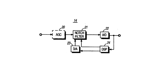
FIG. 2 is a block diagram of the A/D converter and
notch filter 14 in accordance with an embocli~ent of the
35 invention. Include~ within the AID converter and notch
filter 14 is an optional automatic gain control 20, notch
filter 21, A/D ~, D/A 23, and DSP 24 (e.g., a Motorola ~
56000 DSP). The optional AGC may be included within the ''~'J
'
~4~ 2125468
A/D converter and notch filter 14 to maintain an input
signal level below a maximum level allowable by the A/D
22.
Upon application of a Lro&Jl,and signal from the BPF
13 to the AJD converter and notch filter 14 the A/D 22
samples and converts the b~o~L.and signal to digital
samples for application to DSPs 15, 16, and 24. Within -~
DSP 24 the sampled signal is converted from the
frequency domain to the time domain using a fast fourier -
1 0 transform.
Shown in FIG. 3 is an FFT yfaphical represenlalion of
a bru~Land signal applied to the A/D converter and notch -~
filter 14. Include~ within the gr~phical rep~esenlalion of
the bro~lbar..J signal are four radio frequency signals 30
1 5 31, 32 and 33 of four radio channels to be decG-Jed by the
~cei~rer 10. Under the im~anlion the amplitude of the
signals 30, 31 32 and 33 is cG.-"~ar~l with a threshold -
value 35 for a determination of whether the signal 30 31
32, or 33 is to be notch filtered. -- -
Under one e--~bod;,--enl of the invention the ll--esh~ld -
value 35 (FIG. 4) is determined to be 90~/O of the AID 22
full scale input. Upon determination that a signal 40 has
~xcesded the threshold the DSP 24 doter---ines the
location and sp c~.al width of the offending carrier based
upon the results of the FFT. Based upon the spectral
width, loc~iion and magnitude of the offending carrier the
DSP 24 lf~nsFe,s notch filter control para,-,6ters to the
notch filter 21. The peak attenuation of the notch fflter
is determined by the DSP 24 to be at least the Jifforance
between the II.reshold value and the peak of the offending -
carrier 40 at a frequency fO.
The bandwidth of the notch (BWfo) with a center -~
frequency fO is ~eler."ined by the spectral width of the --
sideband noise around the offending carrier. The
bandwidth of the notch is sGl~ct~J to insure that the
attenuation outside the offending carrier bandwidth is
less than the difference in dB of the s;deb~n.J noise around
the ofF6nJing carrier and the thermal noise floor (NF) that
' - 5
is present ahead of the notch filter and A/D. By selecting
the notch bandwidth (and therefore its frequency
response) in this way, the signal to noise ratio of the
other carriers is not degraded beyor,J the value that is
5 inherenl due to the sideband noise of the offendin~
carrier. The peak attenuation and bandwidth are sele~to~
to satisfy the response given in the equalities below,
where atten (fl is the attenuation of the notch fitter at a
frequency (f), A(f) is the amplitude response of the
10 offending carrier at the frequency (f) and NF is a noise
floor (FIG. 4).
Fqu~ffon #1:
atten (f) 2 A(f) - Thresl-old;
1 5
for fo-(BWfo/2)~f<fo 1 (BWfo/2)
:'
F~u~tion #2:
2 0 atten (f) .A(f)-NF;
for fefo-(BWfo/2) or f~fo+(BWfo/2), and --
One of the fundamenbl d;sli"guishing factors of the
invention is that the notch filter response can be s~lecte~l -
to obtain physically realizable values while not causing
signiticant signal to noise degrddaiion to the other
carriers. A critical factor to accG.nplish this is that the
filter response s;~ti~lies F~ tions #1 and 2.
Upon entry of the notch filter parameters into the
notch filbr 21, the DSP 24 then begins fine tuning the
notch filter 21 by application of a control volt~e through
the D/A 23. The control voltage through D/A 23 causes
the center point of the notch to change in frequency based
upon the magnitude of the control voltage. To fine tune
the notch filter 21 to a center fre~uency of the oftdnding
carrier 40, the DSP 24 causes the voltage to sweep
through an area around the centar point of the oflenJ;ny
,
:: :
~ -6- 2125~68
carrier 40 while comparing the FFT output of the A/D 22
with the threshold. Deter,.,in~tion of an optimal control
point is determined by the DSP 24 to be a point where the
or~er,ding carrier amplitude is below the threshold and the
5 notch filter response salisi~es Equation 2.
. ~ . .
; . ., .
: - ~
. ~ ... . .. .... . - . ~ . . .. .