Note: Descriptions are shown in the official language in which they were submitted.
f ~ WO 93/12543 212 5 5 8 o Pcr/Aus2/oo6s8
BURIED C ONTA C J, !NTERCONNECT~D JHIN FILM AND BULK PWOTOVOL TAIC
CELLS
. .
TE~HNICAL FIELD
This inven~ion relates to a semiconductor substrate material having a
photovoltaic cell, a semiconductor substrate material having an integrated
alTay of at least two photovoltaic cells in electrical series with one another,
systems for the production of electricity and methods for the production of
electricity.
BACKGROUND ART
One proposed rnethod for reducing the cost of photovoL~aic energy
. conversion is to deposit the photovoltaic solar cells in the form of a thin sheet
onto a supporting substrate such as glass. Such sheets can be deposited more
or less continuously onto a moving substrate or by other methods. Techniques
are ~en lequired to define individual cells within this deposited sheet and to
provide for their electrical interconnection.
It would be advantageous at least from a manufacturing viewpoint if
the indivildual cells in the substrate cell were such that they could be fabricated
in a wide range of substrate materials, deposition conditions and cell designs.
It would also be advantageous if the inherent features of cells permitted :
relatively large area individual cells and large scale integrated arrays of cells
t~ be fabricated.
OBJECTS OF INVENTION ;
It is an object of this invention to provide a semiconductor substrate
material having a photovoltaic cell, and, a semiconductor substrate material
having an integrated array of at least two photovoltaic cells in electrical series
with one another.
Other objects are to provide systems for the production of electricity
and methods for the production of electricity.
~ - _ISCLOSURE OFINVENTION
According to a first embodiment of this invention there is provided a
serniconductor substrate material having a photovoltaic cell,
said photovoltaic cell comprising~
at least one first type groove having walls doped with a first type
dopant, the first type groove having a first conducting material in
conducting electrical contact with the first type doped walls;
at least one second type groove having walls doped with a second
type dopant, the second type groove having a second conducting
~ -
2125~80
WO 93/12543 - pcr/Aus2/o
rnaterial in conducting electrical contact with the second type doped
walls;
the first and second type grooves being electrically linked with each
other by at least one doped region of linking substrate material
selected from the group consisting of a first type doped region of
linking substrate material and a second type doped region of linking
substrate material, thereby forming a photovoltaic junction where
the doped linking substrate material forms a junction with doped
substrate material of different polarity; and
the first type dopant being of different polarity from the second
type dopant.
According to a second embodiment of this invention there is provided
a semiconductor substrate material having an integrated array of n
photovoltaie cells in electrical series with one another,
each photovoltaic cell being as defined in the ~Irst embodiment;
said n photovoltaic cells in the substrate material being in electrical
series with one another, n being greater than or equal to 2, whereby
an (mj-l~th cell is electrically coupled to an mjth cell via a
configuration selected from the group consisting of~
(i) the first conducting material of the first type groove of an (mj~
l)th cell is electrically coupled via interconnecting conducting
material with the second conducting material of. the second type
groove of an mjth cell; and
(ii) the second conducting material of the second type groove of the
(mj-l)th cell is electrically coupled via interconnecdng conducting
:matedal with the first conducting material of the first type groove
of;the mjth cell;
: ~ :where:j is :greater than or equal to 2 and less than or equal to n and my is
equal: to j~; and~
30 ~ wherein first type doped~ ~walls~ ~of :the first type gr~ove of each
photovoltaic cell in the substrate material are substantially electrically
:; insulated from first :type doped walls of first type grooves of other
photovoltaic cells in the~substrate~material and second type doped walls
of;the second~type groove:of each~photovoltaic cell in the subs~ate
35 ::~ material are substantially electrically insulated from second type doped
: walls of second type grooves of other photovoltaic cells in the substrate
: ~ material.
. .
~ : ~
WO 93/12543 ` - pcr/Au92/oo658
3 21255~0
According to a third embodiment of this invention there is provided a
system for the production of electricity, the system comprising:
(a) a semiconductor substrate ma~erial having a photovoltaic c~ll, in
accordance with the first embodiment; and
S (b) an electrical circuit in electrical communication with the first
conducting material of the first type groove of the cell, and the^ second
conducting material of the second type groove of the cell.
According to a fourth embodiment of this invention there is provided a
system for the production of electricity, the system comprising:
(a) a semiconductor substrate material having an integrated array of n
photovoltaic cells in electrical series with one another, in accordance
with the second embodiment; and
(b) an electrical circuit in electrical communication with conducting
material selected from the group consisting of: ~r
(1) the first conducting material of the first type groove of the first
cell, with the proviso that, except via the electrical circuit, the first
conducting material is not electrically coupled via interconnecting
conducting material with the second conducting material of the
second type groove of another cell in $he electrical series, and
the second conducting material of the second type groove of the
nth cell, with the proviso that, except via the electrical circuit, the
second conducting material is not electrically coupled via
interconnecting conducting material with the first conducting
material of the first type groove of another cell in the electrical
series; and
~2) the second conducting material of the second ~ype groove of the
first cell, with the proviso that, except via the elec~ical circuit, the
second conducting material is not electrically coupled via
interconnecting: conducting material with the ~first conducting
:~ material of the first type~groove of another cell in the electrical
- series, and
the first conducting material of the first type groove of the nth~
: cell, with the proviso that, except via the electrical circuit, the first
conducting matenal is not electrically coupled via interconnecting
conducting material with the second conducting material of the
second type groove of another cell in the electrical series.
According to a fifth embodiment of this invention there is provided a
method for the production of electricity, the method comprising~
,~
Wo 93/125~a3 2 1 2 5 ~ 8 0 P~/AU92/0~
illuminating the junction of the system of third embodiment with light
capable of generating photocurrents at the junction whereby current
flows through the cell thereby loading the electrical circuit.
According to a sixth embodiment of this invention there is provided a
5 method for the production of electricity, the method comprising:
illuminating the junctions of the system of fourth embodiment w;th light
capable of generating photocurrents at the junctions whereby current
flows through the n cells thereby loading the el~ectrical circuit.
The number n of cells may be very large eg 100 and more. Typically
10 an array contains 2 to 5000 cells, more typically 2 to 500 cells or 2 to 100
cells and even more typically 6 to 50 cells or 6 to 2~ cells.
Shunting diodes may be incorporated in the array in accordance with
United States Patent No. 4,323,719 the contents of which are incorporated
herein by crossreference.
15Techniques for the formation of grooves in solar cells are described in
U.S. Patent Nos. 4,748,130 and 4,726,850, the contents of which are
incorporaled herein by cross reference.
Techniques for the solution growth of silicon films are described in
Australian Patent Application No. 31215/89 the contents of which are
20incorporated herein by cross reference.
The first and second type dopants may be n-type, p-type, n+-type or
p~-type dopants with the proviso that the first type dopant is of opposite
polarity to the second type dopant.
The first and second conducting rnaterials can be the same or different
25and can be a metal (eg aluminium), conducting polymer, metal alloy, doped
serniconductors or other appropriate conducting material. Generally the
conducbng material is chosen so that it forms a good electrical contact
~- ~ (pre~elably an ohmic contact) with the walls of the groove(s) with which it is
in contact.
30The photovoltaic cells of the invention are particularly useful in
converting solar light, light from light sources such as tungsten and
fluorescent tubes, photodiodes or lasers into electricity.
T he interconnecting conducting material may be the same or dif~erent
from the first and second conducting materials and can be a metal, conducting
35polymer, metal alloy, doped semiconductor or other appropAate conducting
mateAal.
The semiconductor substrate material can be thin films, single crystal
or polycrystalline material. It may be continuous or discontinuous. Thin films
r_
~ WO 93/12543 pcr/Au92/oo658
2125580
may be supported on a substrate or superstrafe such as glass, quartz, perspex
or other suitable superstrate. When the superstrate is transparent to the
illuminating light the array can be illuminated through the superstrate. The
s miconductor substrate material may be used with appropriate antireflection
5 coatings and fabricated using appropriate antireflec~ion geometries.
Typically, the photovoltaic cell is a solar cell. Semiconductor s^ubstrate
materials such as silicon, germanium, CdTe, CulnSe2, GaAs, AlGaAs, Ga~,
GaAsP, SiC, InP and other photovoltaically active semiconductors are
particularly suitable for p-n photovoltaic cells and particularly for p-n
10 photovoltaic solar cells.
Significant advantages of the present invention are that it provides a
new way of both isolating individual photovoltaic cells in a substrate and of :~
providing electrical interconnection. The technique is applicable to a wider
r;ange of materials deposition conditions and cell designs and allows individual1.~ cells to be much longer (5-25cm) than possible with presently established
photovollaic arrays. The photovoltaic arrays can be of unlimited length since
the highly conductive conducting material in the grooves can carry current
long distances with minimum resistance losses. The substrate or superstrate
provides a high lateral resistance between the lower regions of the grooves of
2~ different cells to ensure effective isolation of ]ike polarity grooves between
individual cells. The technique allows for the use of grooves with thin film
photovoltaic layers and provision of metal contacts to the layers via
conducting material such as metal in the groov~s. A cell can have grooves of
opposite polarity interdigitated with each other to minimise photoactive space
25 lost as well as providing a parallel current path to interconnecting grooves
which interconnect the photovoltaic cells in series and at the same time
providing for low resistance losses.
BF~IEF DESCRUTION OF DRA WINGS
- ~ Fig. l depicts a thin film semiconductor substrate material on a glass
30 superstrate having an integrated array of only two photovoltaic cells in
electrical series with one another in accordance with one embodiment of the
invention;
Fig. 2 depicts alternating n-type and p-type thin film silicon layers on a
supporting glass superstrate and having an oxide or other insulating masking
35 layer on the top n-type silicon layer representing a structure into which an
integrated array of two photovoltaic cells may be formed in accordance with
another embodimen~ of the invention;
¦ SuBsTlTuTE
~ ,
212~8~
WO 93/125'13 ^ PCI'/AIJ92/0
Fig. 3 depicts a cross sectional view of thin film semiconductor substrate
material on a glass superstrate of Fig. 2 having an integrated array of two
phstovoltaic cells in electAcal series with one another;
Fig. 4 depicts a cross sectional view of another type of thin film
semiconductor substrate material on a glass superstrate of Fig. 2 having an
integrated array of two photovoltaic cells in electrical series with one ai~other;
Fig. 5 depicts p~-type layer, i layer and n+-type thin film silicon layers on a
supporting glass superstrate and having an oxide or other insulating masking
layer on top of the p+-type silicon layer;
Fig. 6 depicts a perspective cross sectional view of thin film semiconductor
substrate mateAal on a glass superstrate of Fig. 5 having an integrated array ofphotovoltaic cells in electrical seAes witb one another;
Fig. 7 depicts a plan view of a thin film semiconductor substrate mateAal on a
glass superstrate having an integrated array of three photovoltaic cells in
electAcal seAes with one another in accordance with a further embodiment of
theinvention;
Fig. 8 de~icts a plan view of a thin film semiconductor substrate mateAal on a
glass superstrate having an integrated array of ISve photovoltaic cells in
electAcal seAes with one another in accordance with another embodiment of
the invention;
Fig. 9 depicts a plan view of a thin film semiconductor substrate mateAal on a
glass superstrate having an integrated arMy of four photovoltaic cells in
electrical seAes with one another in accordance with anotber embodiment of
the invention;
Fig. 10 depicts a plan view of a thin film semiconductor substrate mateAal on
a glass superstrate having an integrated array of four photovoltaic cells in
electrical seAes with one another in accordance with another embodiment of
the invention; Fig. 11 depicts a cross sectional view of thin film
semiconductor substrate material on a glass superstrate having an integrated
array of two photovoltaic cells in electrical serAes with one another; and
Fig. 12 depicts a thin film semiconductor substrate material on a glass
superstrate having a photovoltaic cells in accordance with one embodiment of
the invention; ~ .~
BESTMODEAND OTHER MODES FOR CdRRYlNG OUT THE
INVENTlOy
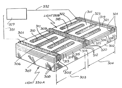
Fig. 1 depicts a thin film semiconductor substrate material 301 on a
glass superstrate 302 having an integrated array of two photovoltaic cells 303
and 304 in electrical series with one another. Photovoltaic cell 303 has
~3 WO ~3/12543 2 12 S 5 8 a PCr/AU92/00658
grooves 305, 306 and 307 each of these grooves having walls doped with a
p+-type dopant as shown at 308 for groove 305. C;rooves 305, 306 and 307
are filled with metal which is in conducting electrical contact with their
respectivep+-type doped walls. Photovoltaic cell 303 also has grooves 310
5 and 311 each oi these grooves having walls doped with a n+-type dopant as
shown at groove 312 being one of the grooves forming double groove 309
which is also part of cell 303. Double groove 309 comprises groove 312 and
groove 320. Groove 320 has walls doped with p+-type dopant and, as already
indicated, groove 312 has walls doped with n+-type dopant. Grooves 310 and
311 and double groove 309 are filled with metal which is in conducting
electrical contact with their respective n+-type doped walls. .
Substrate material 301 in cell 303 includes oxide or other insulating
masking layer 313, p+-type layer 314, intrinsic (which can also be n-type or
p-type) layer 315 and n+-type layer 316. Grooves 305, 306 and 307 are
electrically linked with grooves 309, 310 and 311 by p+-type layer 314, layer
315 (if it is n-type or p-type) and n~-type layer 316 thereby forrning a
photovoltaic junction where the doped linking substrate material forrns a
junction with differently doped substrate material of opposite polarity.
Photovoltaic cell 304 has grooves 318 and 319 each of these grooves
having walls doped with a p+-type dopant as shown at groove 320 for double
groove 309. GrooYes 31~ and 319 and double groove 309 are filled with metal
which is in conducting electrical contact with their respective p+ type doped
walls. Photovoltaic cell 304 also has grooves 321, 322 and 323 each of these
grooves having walls being doped with an n+-type dopant as shown at 324
for groove 321. Grooves 321, 322 and 323 are filled with metal which is in
conducting electrical contact with their respective n+-type doped walls.
Substrate material 301 in cell 304 includes optional oxide or other
insulating masking layer 325, p~-type layer 326, optional intrinsic (which can
also be n-type or p-type) layer 327 and n+-type layer 328. In its simplest
form layers 325 and 327 would not be included, which would mean substrate
material 301 would have 2-layers, namely, p+-type layer 326, and n+-type
layer 328. Grooves 320, 318 and 319 are electrically linked with grooves 321,
322 and 323 by p+-type layer 326, layer 327 (if it is n-type or p-type) and
n+-type layer 328 thereby forming a photovoltaic junction where the doped
linking substrate material forms a junction with differently doped subs~ate
material of opposite polarity.
Photovoltaic cells 303 and 304 in substrate material 301 are in
electrical series with one another since the metal in groove 310 is in electrical
~ ~ .
2`1~ 8 0 8 PC~JAUg2/0~
contact with the metal in groove 318. Grooves 305, 306, 307, 309, 310, 311,
318, 319, 321, 322 and 323 extend near to or are in contact with glass
superstrate 302 so that n+-type doped walls of grooves 309, 310, 311 in cell
303 are substantially electrically insulated from n+-type doped walls of
grooves 321, 322, 323 in cell 304 and p+-type doped walls of grooves 305,
306 and 307 in cell 303 are substantially electrically insulated from p~-type
doped walls of grooves 320, 318, 319 in cell 304.
The high conductivity of the metal in grooves 305, 306, 307, 309,
310, 311, 318, 319, 321, 322 and 323 permits current to be transported over
larger distances than would otherwise be possible, allowing the width of each
cell region 303 and 304 to be very large (eg 20cm).
The metal in grooves 305 and 321 are electrically linked to load 329
via lines 331 and 332.
A preferred substrate material 301 is silicon.
In use light 330A (typically sunlight) passes through glass superstrate
302 or light 330B passes through insulating layer 325 and light of appropriate
wavelength (and which is not reflected) is absorbed by substrate silicon.
Current is photogenerated at the light illuminated p-n junctions in cells 303
and 304 and eventually passes through load 329 via lines 33I and 332.
In an alternative arrangement instead of glass superstrate 302, an
intrinsic, n--type or p~-type single, amoIphous or polycrystalline
semiconductor (intrinsic is preferred) superstrate can be used in its place and
layers 313, 314, 315, 316, 325, 326, 327 and 328 can be either deposited on
substrate 302 or formed from substrate 302 itself. In this instance, unless
superstrate 302 is sufficiently thin, cells 303 and 304 are illuminated via
surface 301.
Referring to Fig. 2 thin film silicon layers 101 and 102 (p-type), 103,
104 and 105 (n-type) are deposited from solution in molten metal by known
techniques onto supporting glass superstrate 107 (other known appropriate
techniques for layer formation may be used). After deposition of these layers
from solution in molten metal, oxide or other insulating masking layer 106 is
either grown or deposited on the surface of layer 103. Suitable techniques for
growing layer 106 include the rapid thermal annealing of the surface region of
the grown layer in an oxygen ambient or the physical vapour deposition or the
chemical vapour deposition of such a layer. A laser is then used to form
grooves 108 and 109, through layers 101, 102, 103, 104, 105 and 106 to, or
approaching, glass superstrate 107 as shown in Fig. 3. Other techniques such
as mechanical scribing or grooving or chemical etching or various
~ SUBSTITUT~ SHEET
~f--) wO 93/l2543 pcr/Au92/oo6s8
9 2~25580 ::
combinations thereof may be used to form the grooves. Additional n-type
material is then deposited onto the entire exposed layer including the walls of
grooves 108 and 109 from metal solution. When additional n-type material is
deposited ~rom metal solution the doped layer may be deposited in such way
S that it forrns selectively in grooved areas since generally growth is more
difficult to nucleate on amorphous oxide or other insulating masking layers.
When additional n-type material is deposited from metal solution or otherwise
onto the entire exposed layer, dopant diffusion is prevented in areas covered
by the oxide or other insulating masking layer but not in the remainder of the
10 grooves. After the deposition, growth or diffusion of the n-type material into
the walls of grooves 108 and 109 to form n+-type doped groove walls 112
and 113 and the removal of unwanted deposited layers, if required by the
details of the particular sequence, an oxide or other insulating masking layer is
grown or deposited onto the walls of grooves 108 and 109 (and onto the
remaining surface layer, if appropriate). Grooves 110 and 111 are then formed
using lasler etching, plasma etching, mechanical scribing or chemical etching
or various combinations thereof through to, or approaching, glass superstrate
107. Additional p-type material is then deposited onto the walls of grooves
110 and 111 in an analogous way to that of the n-type material as described
above to form p~-type doped groove walls 114 and 115. The oxide or other
insulating masking layer is then removed from grooves 108 and 109. Metal is
then deposited to fill grooves 108, 109, 110 and 111 as shown at 116 by a
technique such as electroless plating to form adjacent cells 117 and 118.
Adjacent cells 117 and 118 are interconnected at 119. The p and n regions of
grooves 110 and 109 respectively are physically located very close to each
other.
In Fig. 3 layers 101, 102, 103, 104, 105 and 106 constitute a thin film
semiconductor substrate material on a glass supeirstrate 107 having an
integrated array of two photovoltaic cells 117 and 118 in electrical series withone another. Photovoltaic cell 118 has groove 111 having~walls doped with a
p+-~type dopant as shown at 115. Groove 111 is filled with metal which is in
conducting electrical contact with p+-type doped walls 115. Photovoltaic ~11
118 also has groove lO9 having walls 113 doped with a n+-type dopant)
Groove 109 is filled with metal which is in conducting electrical contact with
n+-type doped walls 113.
Substrate rnaterial in cell 118 includes oxicle or other insulating layer
106, and alternating p-type layers 101 and 102 and n-type layers 103, 104 and
105. Grooves 109 and 111 are electrically linked by layers 101, 102, 103, 104
__
5UC5DrUTC 5~lc~
.
WO 93/12543 212 ~ 5 8 0 . ~ ` pcr/Au92/o~
and 105 thereby forming a photovoltaic junction where the doped linking
layers form junctions with differently doped substrate material of opposite
polarity.
Photovoltaic cell 117 has groove 110 having walls 114 doped with a
5 p~-type dopant. Groove 110 is filled with metal which is in conducting
electrical contact with p+-type doped walls 114. Photovoltaic cell 1'17 also
has groove 108 having walls 112 doped with a n+-type dvpant. Groove 108 is
filled with metal which is in conducting electrical contact with n+-type doped
walls 112.
Substrate material in cell 117 includes oxide or other insulating layer
106, and alternating p-type layers 101 and 102 and n-type layers 103, 104 and
105. Grooves 108 and 110 are electrically linked by layers 101, 102, 103, 104
and 105 thereby forming a photovoltaic junction where the doped linking
layers form junctions with differently doped substrate material of opposite
15 polarity.
Photovoltaic cells 117 and 118 are in electrical series with one another
since the metal in groove 110 is in electrical contact with the metal in groove
109 at 119. Grooves 108, 110, 109 and 111 extel`ld near to glass superstrate
107 so that n+-type doped walls of groove 108 is substantially electrically
20 insulated from n~-type doped walls of groove 109 in cell 118 and any other
n~-type doped walls of grooves of cell 118 or other cells in layers 101, 102,
,103, 104, 105 and 106. Also p+-type doped walls 114 of groove 110 are
substantially electrically insulated from p+-type doped walls 115 of groove
111 in cell 118 and any other p+-type doped walls of grooves of cell 118 or
25 other cells in layers,lOl, 102, 103, 104, 105 and 106.
The high conductivity of the metal in grooves 108, 110, 109 and 111
perrnits current to be transported over larger distances than would otherwise
be possible, allowing the distance between grooves 108 and 110 for cell 117
and the distance between grooves 109 and 111 for cell 118 to be very large
30 (eg 10- 20cm). , ,
Referring to Fig. 4 thin film silicon layers 101 and 102 (p-type), 103,
104 and 10~ (n-type) are deposited from solution in n,olten metal or other
known techniques onto supporting glass superstrate 407. After deposition of
these layers from solution in molten metal or equivalent, oxide or other
35 insulating masking layer 106 is either grown or deposited on the surface of
layer 103. Suitable techniques for growing layer 106 include spraying, screen
printing, the rapid thermal annealing of the surface region of the grown layer
in an oxygen ambient or the physical vapour deposition or the chemical
'
f ) WO93/12~43 212 ~ ~ 8 ~ ; pcr/Au92Joo6s8
11
vapour deposition of such a layer. A laser is then used to form grooves 408
and 409, through layers 10l, 102, 103, 104, 105 and 106 to, or approaching,
glass superstrate 407. Other techniques such as mechanical scribing or
grooving or chemical etching or various combinations thereof may be used to
S form the grooves. Additional n-type material is then deposited onto ~he entireexposed layer including the walls of grooves 408 and 409 from metal solution
or other appropriate or equivalent technique. When additional n-type material
is deposited from metal solution the doped layer may be deposited in such way
that it forms selectively in grooved areas since generally growth is more
10 difficult to nucleate on amorphous oxide or other insulating masking layers.
When additional n-type material is deposited from metal solution Qr otherwise
onto the entire exposed layer, dopant diffusion is prevented in areas covered
by the oxide or other insulating masking layer. Diffusion of the n-type
material into the walls of grooves 408 and 409 forms n~-type doped groove
walls 412 and 413. The deposited layers are then removed if required by the
details of the particular sequence. An oxide or other insulating masking layer
is then grown or deposited onto the walls of grooves 408 and 409 (and onto
the remaining surface layer, if appropriate). Grooves 410 and 411 are then
formed using laser etching, plasma etching, mechanical scribing or chemical
20 etching or various combinations thereof through to, or approaching, glass
superst~ate 407. Additional p-type material is then deposited onto the walls of
grooves 410 and 411 in an analogous way to that of the n-type material as
described above to form p+-type doped groove walls 414 and 415. The oxide
or other insulating masking layer is then removed from grooves 408 and 409.
25 Metal is then depo~sited to fill grooves 408, 409, 410 and 411 by a techniquesuch as electroless plating to form adjacent cells 417 and 418. A~jacent cells
417 and 418 are interconnected at 419 where the p and n wall regions 414 and
413 meet.
In Fig. 4 layers 101, 102, 103, 104, 105 and 106 constitute a thin film
30 semiconductor substrate mateAal on a glass superstrate 407 having an
integrated array of two photovoltaic cells 417 and 418 in electrical series withone another. Photovoltaic cell 418 has groove 411 having walls doped with a
p+-type dopant as shown at 415. Groove 411 is filled with metal which is in
conducting electrical contact with p+-type doped walls 415. Photovoltaic cell
35 418 also has groove 409 having walls 413 doped with a n+-type dopant.
Grooves 409 is filled with metal which is in conducting electrical contact with
n+-type doped walls 413.
a~ .
Wo 93/12543 212 ~i 5 8 r; i ~ pcr/Au92/o6~
Substrate material in cell 418 includes oxide or other insulating layer
106, and alternating p-type layers 101 and 102 and n-type layers 103, 104 and
105. Grooves 409 and 411 are electrically linked by layers 101, 102, 103, 104
and 105 thereby forming a photovoltaic junction where the doped linking
S layers form junctions with differently doped substrate material of opposite
polarity. -
Photovoltaic cell 417 has groove 410 having walls 414 doped with ap+-type dopant. Groove 410 is filled with metal which is in conducting
electrical contact with p+-type doped walls 414. Photovoltaic cell 417 also
10 has groove 408 having walls 412 doped with a n+-type dopant. Groove 408 is
filled with metal which is in conducting electrical contact with n+-type doped
walls 412.
Substrate material in cell 417 includes oxide or other insulating layer
106, and alternating p-type layers 101 and 102 and n-type layers 103, 104 and
105. Grooves 408 and 410 are electrically linked by layers 101, 102, 103, 104
and 105 thereby forming a photovoltaic junction where the doped linldng
layers form junc~ions with differently doped substrate material of opposite
polarity.
Photovoltaic cells 417 and 418 are in electrical series with one another
since the metal in groove 410 is in electrical contact with the metal in groove
409. Grooves 40B, 410, 409 and 411 extend near to glass superstrate 407 so
that n+-typc doped walls of groove 408 is substantially electrically insulated
from n~-type doped walls of groove 409 in cell 418 and any other n+-type
doped walls of grooves of cell 418 or other cells in layers 101, 102, 103, 104,
105 and 106 and p+-type doped walls 414 of groove 410 are substantially
electrically insulated from p+-type doped walls 415 of groove 411 in cell 418
and any other p+-type doped walls of grooves of cell 418 or other cells in
1 ayers 101, 102, 103, 104, 105 and 106.
T he high conductivity of the metal in grooves 408, 410, 409 and 411
permits current to be transported over larger distances ~han would otherwise
be possible, allowing the distance between grooves 411 and 409 in cell 418
andthedistancebetweengrooves410and408incell417tobeverylarge(eg
20cm).
The W-shaped double grooves depicted in Figs. 1 and 4 are produced
by a combination of scribing and chemical etching whereas the U shaped of
Fig. 3 are produced by scribing alone or by scribing and etching wherein the
etching is only slight and sufficient only for pu~poses of cleaning or when the
crystallographic orientation is such as to produce the U shape after substantial
~ ~ ~ .
3 wo 93/12S43 21% 5 5 8 O ~ - pcr/Au92/oo658
13
amounts of appropriate etching. Crystallographic o~ientation may be selected
to give almost any groove shape in conjunction with appropriate scribing and
chemical etching.
Referring to Fig. 5 thin film silicon layers 201 (p+-type), 202 (i or n-
S type3 and 203 (n~-type) are deposited from solution in molten metal or other
known techniques onto a supporting glass superstrate 2M. As an alter~iative to
layers 201, 202 and 203 of the polarities shown in Fig. 5, layers 201, 202 and
203 of Fig. S can be of opposite polarities to those depicted. After deposition
of these layers from solution in molten metal, oxide or other insulating layer
205 is either grown or deposited on the surface of layer 201. Suitable
techniques for growing layer 205 include the rapid thermal annealing of the
surface region of the grown layer in an oxygen ambient or the physical vapour
deposition or the chemical vapour deposition of such layer. A laser is then
used to form grooves 206, 208, 210, 212, 219, 220, 223 and 224 through
1~ layers 201, 202, 203 and 205 to, or approaching, glass superstrate 204 as
shown in Fig. 6. Other techniques such as plasma etching, mechanical
scribing or grooving or chemical etching or various combinations thereof may
be used to form the grooves. Additional n-type material is then deposited onto
the entire exposed layer including the walls of grooves 206, 208, 210, 212,
20 219, 220, 223 and 224 from metal solution or firom doped layers otherwise
deposited thereon. When additiona1 n-type material is deposited from metal
solution the doped layer may be deposited in such way that it forms selectively
in grooved areas since generally growth is more difficult to nucleate on
amorphous oxide or other insulating masking layers. When additional n-type
25 matenal îs deposited from metal solution or otherwise onto the entire exposedlayer, dopant diffusion is prevented in areas covered by the oxide or other
insulatîng masking layer. Diffusion of the n-type material into the walls of
grooves 206, 208, 210, 212, 219, 220, 223 and 224 forms n+-type doped
groove walls~ After removal of deposited layers, if re~quired by the details of
30 the particular sequence, an oxide or other insulating layer or masldng layer is
grown or deposited onto the walls of grooves 206, 208, 210, 212, 219, 220,
223 and 224 (and onto the remaining surface layer, îf appropriate~ Grooves
207, 209, 211, 217, 218, 213, 221 and 222 are then formed using laser
etching, plasma etching, mechanical scribing or chemical etching or various
35 combinations thereof through to, or approaching, glass superstrate 204~
Additional p-type material is then deposited onto the walls of grooves 207,
209, 211, 217, 218, 213, 221 and 222 in an analogous way to that of the n-
type material as described above to form p+-type doped groove walls.
SUBSTITUTE SHEET
wO 93/l2543 2 ~ 2 ~ ~ ~ O i 14 PCr/AU92/oO~ ~
Grooves 210 and 211 together form W-shaped double groove 215 and grooves
212 and 213 together form W-shaped double groove 214. By appropriate
geometrical layout as shown in Fig. 6, the n+-type regions and p~-type
regions can either act as sites for defining the boundaries of individual cells
(grooves 210 and 212 for n~-type and grooves 211 and 213 for p+-type) or
merely as contact regions for such cells (grooves 206, 208, 219, 220, 223 and
224 for n+-type and grooves 207, 209, 217, 218, 221 and 222 for p+-type).
The masking layer is then removed from grooves 206, 208, 210, 212, 219,
220, 223 and 224. Metal is then deposited to fill or partially fill grooves 206,208, 210, 212, 219, 220, 223, 224, 207, 209, 211, 217, 218, 213, 221 and
222 by a technique such as electroless plating. The high conductivity of such
deposited metal allows current to be transported over larger distances than
would otherwise be possible, allowing the width of each cell region 216 to be
very large (eg 20cm) as shown in Fig. 6. Adjacent cells are interconnected
where metal in adjacent grooves (eg grooves 210 and 211) meets.
It ~ill be apparent from Fig. 6 that multiple photovoltaic cells in series
can be constructed on a single superstrate or substrate. In this regard, for
example, reference is made to Figure 7 which depicts a plan view of a system
700 for tl!e production of electricity compAsing a thin film semiconductor
20 substrate rnaterial 705 on a glass superstrate (not shown) having an integrated
array of three photovoltaic cells 701, 702 and 703 in electrical series with oneanother. In system 700, load 704 is in electrical communication with
conducting material 707 of a first type groove of cell 701 via line 706 and a
second conducting material 708 of a second type groove of cell 703 via line
709 except via lines 706 and 709 and load 704. The black areas 707, 708, 710 ~ ^
and 711 in system-700 depict conducting material in grooves of the types
shown in Fig. 6 and are not drawn to scale. In system 700, conducting
material 707 is not electrically coupled via interconnecting conducting materialwith conducting material of a~second type groove of cell 702 or 703. In
addition, in system 700 conducting material 708 is not electrically coupled via
interconnecting conducting material with conducting material of a first type
groove of cell 702 or 701 except via lines 706 and 709 and load 704.
As another example that multiple photovoltaic cells in series can be
constnucted on a single superstrate or substrate, reference is made to Figure 8
which depicts a plan view of a system 800 for the production of electricity
comprising a thin film semiconductor substrate material 806 on a glass
superstrate (not shown) having an integrated array of five photovoltaic cells
801, 802, 803, 804 and 805 in electrical series with one another. In system ~ ~
", :
SUCSIITII~ SHEET :: :
;~-,
f )wo93/12543 ' ` ` PCr/AUs2/00658
800, load 809 is in electrical communication with conducting material 807 of ;~
a first type groove of cell 801 via line 808 and a second conducting material
811 of a second type groove of cell 805 via line 810. The black areas 807,
812, 813, 814, 815 and 811 in system 800 depict conducting material in
5 grooves of the types shown in Fi~g. 6 and are not drawn to scale. In system
800, conducting material 807 is not electrically coupled via interconnecting
conducting material with conducting mate~ial of a second type groove of cell
802, 803, 804 or 805 except via lines 808 and 810 and load 809. In addition,
in system 800 conducting material 811 is not electrically coupled via
10 interconnecting conducting material with conducting material of a first type
groove of cell 804, 803, 802 or 801 except via lines 808 and 810 and load
809.
As a further example that multiple photovoltaic cells in series can be
constructecl on a single superstrate or substrate, reference is made to Figure 915 which depicts a plan view of a system 900 for the production of electricity
comprising a thin film semiconductor substrate material 906 on a glass
superstrate (not shown) having an integrated array of four photovoltaic cells
901, 902, 903 and 904 in electrical series with one another. In system 900,
load 909 is in electrical communication with conducting material 907 of a first
20 type groove of cell 901 via line 908 and a second conducting material 911 of a
æcond type groove of cell 904 via line 910. The black areas 907, 912, 913,
914 and 911 in system 900 depict conducting material in grooves of the types
shown in Fig. 4 and are not drawn to scale. In system 900, conducting
matenal 907 is not electrically couple~i via interconnecting conducting material25 with conducting material of a second type groove of cell 902, 903 or 904
except via lines 908 and 910 and load 909. In addition, in system 900
conducting material 911 is not electrically coupled via interconnecting
- conducting matenal with conducting material of a first type groove of cell
903, 902 or 901 except via lines 908 and 910 and load 909.
As yet a further example that multiple photovoltaic cells in series can
be constructed on a single superstrate or substrate, reference is made to Figure10 which depicts a plan view of a system 1000 for the production of electricity
comprising a thin film semiconductor substrate material 1006 on a glass
superstrate (not shown~ having an integrated array of four photovoltaic cells
1001, 1002, 1003 and 1004 in electrical series with one another. In system
1000, load 1009 is in electrical communication with conducting material 1007
of a first type groove of cell 1001 via line 1008 and a second conducting
material 1011 of a second type groove of cell 1004 via line 1010. The black
j SUBSTITUTE SHEET :~:
WO 93/12543 212 ~ 5 8 0 PCI'/AU92/0~
1 6
areas 1007, 1013, 1014, 1015 and 1011 in system 1000 depict conducting
material in grooves of the types shown in Fig. 3 and are not drawn to scale. In
system 1000, conducting material 1007 is not electrically coupled via
interconnecting conducting material with conducting material of a second t~ype
S groove of cell lQ02, 1003 or 1004 except via lines 1008 and 1010 and load
1009. In addition, in system 1000 conducting material 1011 is not elec~rically
coupled via interconnecting conducting material with conducting material of a
first type groove of cell 1003, 1û02 or 1001 except via lines 1008 and 1010
and load 1009.
One of the advantages of the approach of Figs. 3 or 4 is that the thin
film semiconductor substrate material may simply have one n-type layer and
one p-type layer electrically interlinking the p+-type and n+-type grooves in
each cell or may have a plurality of n-type layers and p-type layers which
alternate with one another as shown in Figs. 3 and 4, for example, electrically
interlinking the p+-type and n+-type grooves in each cell. For instance there
may be 20 or more n-type layers and 20 or more p-type layers which alternate
with one another as shown in Figs. 3 and 4, for example, electrically
interlinking the p+-type and n+-type grooves in each cell. It is appropriate in
view of l:he relative simplicity of a photovoltaic cell having one n-type layer
and one p-type layer electrically interlinking the p+-type and n+-type
grooves in each cell to describe such a cell in more detail with reference to
Fig. 11. In Fig. ll layers 1101, 1102 and 1103 constitute a thin film
semiconductor substrate material on a glass superstrate 1107 having an
integrated array of two photovoltaic cells 1117 and 1118 in electrical seAes
with one another. Photovoltaic cell 1118 has groove 1111 having walls doped
with a p+-type dopant as shown at 1115. Groove 1111 is filled with metal
which is in conducting e]ectrical contact with p+-type doped walls 1115.
Photovoltaic cell 1118 also has groove 1109 having walls 1113 doped with a
n+-type dopant3. Groove 1109 is filled with metal which is in conducting
electrical contact with n+-type doped walls 1113.
Substrate material in cell 1118 includes oxide or other insulating layer
- 1101, and n-type layer 1102 and p-type layer 1103. Grooves 1109 and 1111
are electrically I inked by layers 1102 and 1103, thereby forn~ing a
photovoltaic junction where the doped linking layers form junctions with ~`
differently doped substrate material of opposite polarity. .
Photovoltaic cell 1117 has groove 1110 having walls 1114 doped with
a p+-type dopant. Groove 1110 is filled with metal which is in conducting
electrical contact with p+-type doped walls 1114. Photovoltaic cell 1117 also
~ , ~
) Wo 93~12543 ~ ~ pcr/Au92/oo6~8
17 21255~0 : ~
has groove 1108 having walls 1112 doped with a n+-type dopant. Groove
1108 is filled with metal which is in conducting electrical contact with n+-
type doped walls 1112.
Substrate material in cell 1117 includes oxide or other insulating layer
S 1101 n-type layer 1102 and p-type layer 1103. Grooves 1108 and 1110 are
electrically linked by layers 1102 and 1103, thereby forming a photo`voltaic
junction where the doped linking layers form junctions with differently doped
substrate material of opposite polarity.
Photovoltaic cells 1117 and 1118 are in electrical series with one
another since the metal 1116A in groove 1110 is in electrical contact with the
metal 1116B in groove 1109 via metal bridge 1119. Grooves 1-108, 1110,
1109 and 1111 extend near to glass superstrate 110,' so that n+-type doped
walls of groove 1108 is substantially electrically insulated from n+-type
doped wa]lls of groove 1109 in cell 1118 and any other n+-type doped walls
of groove~s of cell 1118 or other cells in layers 1101, 1102 and 103. Also p+-
type doped walls 1114 of groove 1110 are substantially electrically insulated
from p+-type doped walls 1115 of groove 1111 in cell 1118 and any other
p+-type doped walls of grooves of cell 1118 or other cells in layers 1101,
1102 and 1103.
The high conductivity of the metal in grooves 1108, 1110, 1109 and
1111 permits current to be transported over larger distances than would
otherwise be possible, allowing the distance between grooves 1108 and 1110
for cell 1117 and the distance between grooves 1109 and 1111 for cell 1118 to
be very large (eg 10 - 20cm).
Fig.. 12 depicts a thin film semiconductor substrate material
1301 on a glass superstrate 1302 having a photovoltaic cell 1303. Photovoltaic
cell 1303 has grooves 1305, 1306 and 1307 each of these grooves having
walls doped with a p+-type dopant as shown at 1308 for groove 1305.
Grooves 1305, 1306 and 1307 are filled with metal which is in conducting
electrical contact with their respective p+-type doped walls. Photovoltaic oell
1303 also has grooves 1310 and 1311 each of these grooves having walls
doped with a n+-type dopant as shown ~or groove 1312 at 1324. Grooves
1310, 1311 and 1321 are filled with metal which is in conducting electrical
contact with their respective n +-type doped walls.
Substrate material 1301 in cell 1303 includes oxide or other insulating
masking layer 1313, p+-type layer 1314, intrinsic (which can also be n-type
or p-type) layer 1315 and n+-type layer 1316. Grooves 1305, 1306 and 1307
are electrically linked with grooves 1310, 1311 and 1321 by p+-type layer
~UE~ST~TUTE SHEET
WO 93/12543 212~ 0 PCr/AU92/0
18
1314, layer 1315 (if it is n-type or p-type) and n~-type layer 1316 thereby
forming a photovo]taic junction where the doped linking substrate material
forms a junction with differently doped substrate material of opposite polari~.
In its simplest form layers 1314 and 1314 would not be included which would
5 mean substrate material 1301 would have 2-layers, namely, p+-type layer
1314, and n~-type layer 1316. The high conductivity of the nietal in
grooves 1305, 1306, 1307, 1310, 1311 and 1321, permits current to be
transported over larger distances than would otherwise be possible, allowing
the width of cell region 1303 to be very large (eg 20cm).
The metal in grooves 1305 and 1321 are electrically linked to load
1329 via lines 1331 and 1332.
A preferred substrate material 1301 is silicon.
In use light 1330A (typically sunlight) passes through glass superstrate
1302 or light 1330B passes through insulating layer 1313 and light of
appropr.iate wavelength (and which is not reflected) is absorbed by substrate
silicon. Current is photogenerated at the light illuminated p-n junctions in cell
13~3 and eventually passes through load 1329 via lines 1331 and 1332.
In an alternative arrangement instead of glass superstrate 1302, an
intrinsic, n~-type or p~-type single, amorphous or polycrystalline
semiconductor (intrinsic is preferred) superstrate can be used in its place and
layers 1313, 1314, 1315 and 316, can be either deposited on substrate 1302 or
formed from substrate 1302 itself. In this instance, unless superstrate 1302 is
sufficiently thin and cell 1303 is illuminated via surface 1301.
It will be rea~lily apparent to a person skilled in the art from the
systems depicted in Figures 1, 3, 4, 6, 7, 8, 9, 10 and 11 that systems with a
large number of photovoltaic cells in electrical series with one another can be
constructed in an analogous manner to those depicted.
It will be recognized by persons skilled in the art that numerous
va~iations and modifications may be made to the invention as described
without departing from the spirit or scope of the invention as broadly -
described. For example, the techniques described are not only applicable to
silicon and amorpholls silicon substrates, but are applicable to any
semiconducting substrate which may be used in a photovoltaic device.
Deposited layers and substrates may not be substantially flat as shown
but may include texture or patterns to reduce reflection from cell surfaces and
also trap light into the ce]l. ;;
SUBSTITU~. S~EET i
~ , rj