Note: Descriptions are shown in the official language in which they were submitted.
21~(i~J
Case 1050
,~7I~GNOSTI.C CIRCUTT AND METHOD FOR AMPEROMETRZCALLY
DETERMINING THE CURRFNT PASSING THRO 3 ~H A EN,~c R
This invention relates generally to araperometric
circuits and methods of analysis, and more particularly to
diagnostic circuits and methods of analysis for
amperometrically determining the current passing though a
sensor. The invention is suitable for use in amperometric
analysis using a disposable electroanalytical sensor for
the quantitative determination of biological compounds
such as glucose from body fluids, and it will be
convenient to hereinafter disclose the invention in
relation to that exemplary application. It is to be
appreciated, Yaowever, that the invention is not limited to
that application.
Diabetes is a metabolic disease characterised by
deficient insulin production by the pancreas which results
in abnormal levels of blood glucose. With daily injections
of insulin, and strict control of dietary intake, the
patient's blood sugar level can be properly maintained.
However, the blood glucose level must be closely followed
in the patient either by clinical laboratory analysis or
by daily analysis which the patient can conduct using
relatively simple, non-technical methods.
One such method for monitoring a patient's blood
sugar level involves the use of sensors comprising at
least a reference electrode and a working electrode coated
with a mixture of,a catalytically active, enzyme arid a.
mediator compound (and possibly further coated with a
retaining permeable membrane). When such a coated
electrode is placed in contact with a substrate containing
a substance for which the enzyme exerts a catalytic
effect, the mediator compound transfers charge to the
electrode. An effective measure of the charge transfered
at an certain specified time after the instant of
application of a constant potential across the sensor, is
21~~?~~~
2
found to be proportional to the glucose concentration in
the blood sample.
Figure 1 shows an existing diagnostic circuit 1 for
measuring the current passing through such a sensor 2. The
diagnostic circuit 1 comprises a reference voltage source
3, an operational amplifier 4, a low-pass filter 5 and an
analog/digital converter 6. The reference voltage source 3
comprises three resistors 7, 8 and 9 and a diode 10. The
resistor 7 is connected at one end to a voltage supply V+
and at the other end to the anode of the diode 10:~ The
cathode of the diode 10 is connected to a ground supply,
whilst the resistors 8 and 9 are connected together in
series across the diode 10. The diode 10 thus conducts,
the resistors 8 and 9 acts as a voltage divider of the
Voltage between the terminals of the diode 10 so as to
supply a reference voltage Vref of 300 mV to the non-
inverting input of the operational amplifier 4.
One electrode of the sensor 2 is connected to the
inverting input of the operational amplifier 4, whilst its
other electrode is connected to the ground supply. A
feedback resistor 11 having a value R11 is connected
between the output and the inverting input of the
operational amplifier 4. The current I flowing in the
resistor 11 is thus equal to ~rel/Rl. Due to the virtual
ground between the inverting and non-inverting inputs of
the operational amplifier 4, the same current I flowing
through the resistor 11 also flows through the sensor 2.
From knowledge of ahe value R11 of the resistor 11, the
value of the current I flowing across the sensor 2 may be
determined by measuring the voltage drop across the
resistor 11.
The low-pass filter 5 comprises a capacitor 12 and
resistor 13, which are connected together in series across
the resistor 11 to remove noise or other interference from
the voltage signal across the resistor 11.
21~~?~~
3
The analog/digital converter 6 comprises an AND gate
14, a comparator 15, a binary counter a.6 and a
digital/analog converter 17. The voltage drop across the
capacitor 12 is applied to the inverting input of the
comparator 15, whilst the output of the comparator 15 is
connected to one input of the AND gate 14. A clock signal,
referenced CLOCK is supplied to the other input of the AND
gate 14 by a convenient timing circuit (not shown) . The
counter 7.6 counts output pulses received from the AND gate
14, the number of pulses counted being represented in
binary form by the logical state of the its outputs 16a,
16b, 16c and 16d. In this arrangement, the state of the
output 16a respresents the most-significant-bit and 16d
represents the least-significant-bit.
The digital/analog converter 17 comprises four
digital switches 18, 19, 20 and 21 each having an control
input connected to one of the outputs 16a to 16d of the
counter 16 and two inputs repectively connected to ground
and to the voltage supply V+. Each of these digital
switches 18 to 21 is arranged so that, according to the
high or low logic level of the output 16a to 16d to which
its control input is connected, its output is connected to
either the supply voltage V+ or to ground.
The output of each of the switches 18 to 21 is
connected by means of a resistor 22, 23, 24 and 25
respectively to the inverting input of an operational
amplifier 26. The non-inverting input of this operational
amplifier is connected to the ground and,its output, is
connected both to its inverting input via a feedback
resistor 27 and to the inverting input of the comparator
15.
The .resistors 22, 23, 24 and 25 have the values R,
2R, 4R and 8R, so that a high at the outputs 16a, 16b, 16c
and 16d causes a voltage of 8V, 4V, 2V and V respectively
to be applied to the inverting input of the operational
amplifier 26 where V is the value of the voltage applied
._.,
4
to the inverting input of the operational amplifier 26
when only the output 16d of the counter 16 is in a
logically high state. A voltage corresponding to the sum
of the voltages applied to its inverting output is
provided at the output of the operational amplifier 26.
This voltage is compared by the comparator 1S with the
voltage across the capacitor 12.
Initially, the counter 12 is set to zero, and each of
its outputs 16a, 16b, 16c and 16d is low. The sum of the
voltages applied to the inverting input of the operational
amplifier 26, and the voltage at the inverting input of
the comparator 15, is at zero volts. In these conditions,
the output of the comparator 15 is high and the AND gate
14 transmits the clock signal CLOCK to the counter 16. The
counter 16 records the number of clock pulses received
from the AND gate 14. The binary number at the outputs
16a, 16b, 16c and 16d, representing the number of pulses
counted increases linearly with time, is used as the input
of the D/A converter 17. The output voltage of the D/A
converter 17 increases by steps and has, at each instant,
a value corresponding to the sum of the voltages applied
to the inverting input of the operational amplifier 26.
As long as the voltage across the capacitor 12 is
greater than the voltage at the output of the operational
amplifier 26, the output of the comparator 15 is at a high
logic level and the AND gate 14 transmits the clock pulses
of the signal CLOCK to the counter 16. When the voltage at
the output of the, operational amplifier 26 exeeeds,the
voltage across the capacitor 12, the comparator output
passes to a low logic level, which blocks the AND gate 14
and interrupts the counting of the the clock pulses CLOCK.
At this moment, the voltage across the capacitor 12 and
the voltage at the output of the operational amplifier 2.6
are approximately equal and the logical states of the
outputs 16a, 16b, 16c and 16d of the counter 16 represent
a binary number 28, which is a measure of the voltage at
2~.2~~~~
the terminals of the capacitor 12. As the value of the
resistor 11 is known, the binary number 28 equally
representative of the value of the current I passing
through the sensor 2.
The diagnostic circuit 1 shown in figure 1 is
basically analog in nature and requires the use of two
operational amplifiers 4 and 26, in addition to the
numerous other circuits circuit elements described above,
to produce a digital output signal representative of the
resistance of the sensor 2. 2n order to accurately measure
the glucose level in the blood sample placed on the
sensor, the operational amplifiers 4 and 26 must have
excellent DC, small-signal and transient performance and
have a highly linear transfer characteristic. In order to
achieve such performance, it is often the case that twenty
or more transistors as well as several resistive and
capacitive circuit elements are required to realise each
one of the operational amplfiers 4 and 26. Such designs,
which maintain the desired parameters of the amplifier,
are also difficult to accurately realise as integrated
circuits.
An object of the present invention is to provide a
diagnostic circuit for amperometrically determining the
current passign through a sensor which alleviates or
overcomes the disavantages of the prior art.
With that object in mind, one aspect of the present
invention provides a diagnostic circuit for
amperometrically determining the current passing though a.
sensor, comprising a current source for passing a constant
DC current through said sensor, switching means for
selectively operating said current source, comparing means
for comparing the potential difference across said sensor
to a reference voltage and for producing a control signal
having a a first logic level when said potential
difference is less than said reference voltage and a
second logic level when said potential difference is
~.~~G~~~~~
6
greater than said reference voltage, control means for
providing a switching signal having said first logic level
or said second logic level depending upon said control
signal having said first or said second logic level, said
switching means being caused to operate when said
switching signal has said first logic level, and timing
means for measuring the cumulative time passed by said
switching signal in the first logic level during a
selected time interval, so as to provide an output signal
indicative of the mean value of said current passing
through said sensor.
A diagnostic circuit is therefore provided in which
the number of circuit components is minimized and which
does not require the complex and highly accurate circuitry
of existing diagnostic circuits. The diagnostic circuit of
the present invention is accordingly more easily realised
in the farm of an integrated circuit.
Another aspect of the present invention provides a
method of amperometrically determining the current passing
though a sensor using a diagnostic circuit having the
current source, switching means, comparing means, control
means and timing means described above, characterised in
that it comprises the steps of
(a) replacing said sensor with a calibration element of
known resistance,
(bD measuring a first cumulative time passed by said
switching signal in said first logic level during said
selected time interval. so as to determine. a calibration.
factor,
(c) replacing said calibration element with said sensor,
(d) measuring a second cumulative time passed by said
switching signal in said first logic level during said
selected time interval,
(e) muliplying said second cumulative time by said
calibration factor so as to provide an output signal
v ~~.lI~~~G
7
indicative of the mean value of current passing through
said sensor.
In this way, the diagnostic circuit may be calibrated
so that its output signal is independant of the actual
value of current supplied by the constant current source.
The following description refers in more detail to
the various features of the present invention. To
facilitate an understanding of the invention, reference is
made in the description to the accompanying drawings where
the diagnostic circuit is illustrated in a preferred
embodiment. It is to be understood that the circuit and
method of the present invention are not limited to the
preferred embodiment as illustrated in the drawings.
In the drawings:
Figure 1, already described, is a simplified circuit
diagram of an existing diagnostic circuit;
Figure 2 is a simplified circuit diagram of an
embodiment of the diagnostic circuit according to the
present invention; and,
Figure 3 is a timing diagram showing the
interrelation between various signals of the circuit of
figure 2.
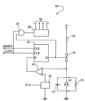
Referring now to figure 2, there is shown generally a
diagnostic circuit 40 for amperometrically determining the
current passing through a sensor 41. The circuit 40
comprises basically a comparator 42, a reference voltage
supply 43, a D-latch 44, an analog gate 45, a load
resistor 46, a capacitor 47, a counter 48 end an AND gate.
49. The load resistor 46 is connected at one end to a
voltage supply V+ and at the other end to the one
electrode of the sensor 41 via the analog gate 45. The
other electrode of the sensor 41 is connected to a ground
supply. The capacitor 47 is connected in parallel across
the sensor 41. When the analog gate 45 conducts, current
is caused flow through the the sensor 41 and the capacitor
47.
8
The potential difference Vas across the sensor. 41 is
compared by the comparator 42 to a reference voltage of,
for example, 300 mV from the reference voltage supply 43.
The output of the comparator 42 is high when the potential
difference VBS across the sensor 41 is less than the 300 mV
refernce voltage and low when the potential difference V$s
across the sensor 41 is greater than the 300 mV refernce
voltage.
The comparator autput 42 is connected to the D input
of the D-latch 44. A clock signal CLOCK, comprising a
series of pulses evenly spaced in time and having, for
example, a frequency of 32768 pulses/second, is supplied
to the clock input CLK of the D-latch 44. The Q output of
the D-latch 44 takes, at the end of each clock pulse
CLOCK, the high or low logic level of the signal supplied
to the D input at the start of that clock pulse. The state
of the Q output is maintained between consecutive clock
pulses.
The D-latch 44 also has a reset input, to which is
supplied an enable signal EDIABLE by a control circuit (not
shown in figure 2). When the enable signal is low, the Q
ouput of the D-latch 44 is held low. Conversely, when the
enable signal ENABLE goes high, the state of the signal at
the D input of the D-latch 44 at the start of each clock
pulse is transferred to its Q output at the end of that
clock pulse.
The Q output of the D-latch 44 is supplied to the
analog gate 45 is order to control the operation thereof.
The analog gate 45 is open, and thereby allows current to
flow through the sensor 41, when the Q output of the D-
latch 44 is high. In this state, the resistance of the
analog gate 45 is substantially less than the load
resistor 46. The current supplied to the sensor 41 is thus
determined essentially by the values of the voltage V+ and
of the resistor 46.
9
When the Q output of the D-latch 44 is low, the
analog gate 45 remains closed and prevents the flow of
current through the sensor 41. In this way, the operation
of the analog gate 45 is controlled so that it remains
either open or closed for at least the period of one clock
cycle. It can be see m that the voltage V-~ and the
resistor 46 form a current source which is controlled by
means of the analog gate 45 and the signal present at the
Q output of the D-latch 44. The use of the D-latch 44
prevents the diagnostic circuit 40 from entering a race-
around condition where the comparator output and the
open/closed state of the analog gate oscillate rapidly
back and forth and are thus ambiguous. It is to be
appreciated that alternative means, such as an R-S flip-
flop or other suitable circuit, may be used to control the
operation of the current source's switching means.
The Q output of the D-latch 44 and the clock signal
CLOCK are logically combined by the AND gate 49, whose
output is connected to the counter 48. The saunter 48 thus
counts the number of clock cycles when the Q output of the
D-latch is high. The output 50 of the counter 48 provides
binary number of the total time during which the Q
output is in the logically high state. This total time is
representative of the resistance of the sensor 41 as will
be become clear from the following. Other timing means for
measuring the cumulative duratiion of the high state of
the Q output will be apparent to one skilled in the art.
The operation ,of the diagnostic circuit 40 will :now
be explained with respect to figure 3, cahich shows a
timing diagram of the clock signal CLOCK, the enable
signal ENABLE, the Q output of the D-latch 44, the
potential difference Vgs across the sensor 41 and the D
input of the D-latch 44 described in relation to figure 2,
At a time tp, the enable signal ENABLE goes from a low
state to a high state. As the analog gate 45 is closed, no
current flows through the sensor 41 and the potential
~1~~~~~
difference VBS thereacross is zero volts. Under these
conditions, the output of the comparator 42 is high.
At the end of the next clock pulse, at time t1, the
high state of the D input is transferred to the Q output,
and the analog gate 45 conducts. Current is thus caused to
flow through the resistor 46, the capacitor 47 and the
sensor 41. As the current continues to flow, the capacitor
47 is charged and the potential difference Vns across the
sensor 41 increase with time. For as Long as this
potential difference remains less than the refarnce
voltage of 300 mV, the D input remains high, as does the Q
output, and the analog gate 45 continues to conduct. In
addition, during this time, the counter 48 counts the
clock pulses transmitted to it by the AND gate 49.
In other embodiments of the present invention, the
capacitor 47 may be omitted from the diagnostic circuit
40, the increase over time of the potential difference
across the sensor 41 being due to the internal capacitance
of the sensor itself.
At time t2, the potential difference VBS across the
sensor 41 reaches the value of 300 mV. The output of the
comparator 42, and hence the D input, pass to the
logically low level. At the end of the next clock pulse,
at time t3, the Q output passes to the logically low
level, thereby blocking the analog gate 45 and prevent
current from flowing through the sensor 41. In addition,
the AND gate 49 blocks the transmission of the clock
pulses to the counter 48, which temporarily stop s
counting.
As current no longer flows from the voltage supply V+
and the resistor 4&, the capacitor 47 discharges over time
until, at a time t4, the potential difference VBS across
the sensor 41 falls to below the reference voltage of 300
mV. The comparator output and the D input therefore change
from a low level to a high level. At the end of the next
clock pulse, at time t5, the Q output passes to a high
7.1
level thereby causing the analog gate 45 to conduct and
current to again flow through the resistance 46 and to the
capacitor 47 and the sensor 41. The AND gate 49 is once
again able to transmit the clock signal CLOCK to the
counter 48, which recommences counting. The capacitor 47
is again charged by the current supplied via the voltage
supply V+ and the resistor 46, so that the potential
difference VBS across the sensor 41 again increases over
time.
This process continues, the analog gate 45 passing
alternatively between blocked state and its conducting
state and vice-versa at the times t6 to t12 as represented
in figure 3. The potential difference VBS across the sensor
41 thus oscillates around the value of 300 mV.
During the periods when the analog gate 45 conducts,
the current IHS flowing in the resistor 46, after time to,
is given by
Ias = ~V+ - Vxee) /RQs
where Vree iS the reference voltage of 300 mV and R46 is the
value of the resistor 46. This value R46 is invariable, so
that a constant current source is effectively provided for
supplying a constant current to the sensor 41. The
operation of this constant current source is controlled by
the analog gate 45. In other embodiments of the invention,
other realisations of a switchable constant current source
may be used in place of that shown.in figure 2, as will be
appreciated by those skilled in the art. Further, the
switching means for selectively operating the constant
current source may be realised other than by the analog
gate 45.
The proportion of time during which the analog gate
46 was open is can be found by the ratio NQ1/ ~NQ2 + NQO)
where NQ1 is the total number of clock pulses which are
counted by the counter 48 during the measurement time,
12
this number NQ1 being thus representative of the total
time during which the analog gate 45 was open over the
measurement period and NQO is the number of clock pulses
which were not counted by the counter 48 during the
measurement period, this number NQO being representative
of the totoal time during which the analog gate 45 was
closed during the measurement time. The sum of the numbers
NQ1 and NQO is obviously representative of the duration of
the measurement period.
The mean current IHSave flowing to the sensor 4~ and
capacitor 47 is therefore given by
IRSave = [ (V+ - Vref) /Ras] * [NQ1/ (NQ1 + NQO) l .
As the values of V+, Vref, R~s and (NQ1 + NQO ) are
predeterminable, the number NQ1 is representative of the
mean current IBSave passing through the sensor 41 during
the selected measurement interval.
Preferrably, the diagnostic circuit 40 shown in
figure 2 can be calibrated to account for possible
variations in the value of constant current caused by a
change in the value of V+ over time and/or any
manufacturing variation in the value R96 of the resistor
46. For example, if the voltage V+ is supplied by a power
source such as a battery, it is known that the actual
value of the voltage V+ will significantly fall over an
exended period of time. Similarly, the precise value of
the resistor 46 RQ;may vary from one circuit to the next
by ~50 or more, depending upon manufacturing variations.
Even though the absolute values V+ and R46 may not be known
with precision, they are nevertheless stable within a
period of some hours. During a measurement period of some
dozens of seconds, these values may be considered to be
invariable.
In order to calibrate the diagnostic circuit 40 to
eliminate the effect of the variation in the values of V+
13
and R~6, the sensor 41 may be replaced by a precision
resistor 51 having a value R~a~ . Such a resistor can be,
for examp7.e, wire-wound and have a tolerance of ~0.050 or
better. The mean current I~eiave flowing through the
resistor 51 is given by
I~alave = [ (V+ - V=ef) /R9s] * [NQlca1/ ~NQlca1 + NqOcal) ~
where NQlca1 is the total number of clock pulses counted
while the analog gate 45 conducts during the measurement
time and NQ0ca1 is number of clock pulses occuring while
the analog gate 45 is blocked during the measurement
time. From this it follows that
(V+ - Vree) /Ras = (~lr~r*NQcal) / (R~al*NQlca1) = Xcal
where NQcal = (NQlca1 -~ NQOcal) and Xcal is the calibration
factor of the diagnostic circuit 40. As Vref and R~a~ are
known, the calibration factor Xca1 is obtainable directly
from the output of the counter 48 for a selected
measurement time corresponding to NQcal clock pulses.
After the determination of the calibration factor
Xcal, the precision resistor 51 is replaced by the sensor
41 and the mean current I$Save flowing through the sensor
41 is measured as described above. The actual value of the
resistance of the sensor 41 to which the binary number 50
corresponds is obtained by dividing the binary number 50
by the calibration,factor Xcal. This can be understood by
considering that the mean current IBSave flowing through
the sensor 41 is given by
IBSave = ( (V+ -Vref) /Rqs] * (NQlmes/NQmes) = Xcal* (NQlmes/NQmes)
where NQlmes is the number of clock pulses counted, once
the precision resistor 51 has been replaced by the sensor
41, during the total time when the analog gate 45 conducts
~.~26~9~
1. 4
during the measurement time and NQOmes is the corresponding
number of clock pulses occuring when the analog gate 45 is
blocked. The mean current IBSave passing through the sensor
41 may therefore be measured in a way which is independant
of any variation in the values of V+ and RAS-
If the value R46 of the resistor 46 is known with
precision, the above-described calibration step, in which
Xcal is determined, enables the actual value of V+ to
addtionally be determined from a calculation of
V+ _ (Xcal*Rqb) - Vree
which value may be used as a battery "end-of-life"
detector to detect when the value V+ falls below a
selected threshold, indicating that the battery should be
replaced.
The diagnostic circuit 40 may also be used in
applications requiring the measurement of temperature. An
Negative-Temperature-Coefficient or NTC sensor, having a
resistance which varies in a known way with temperature,
may be used in place of the sensor 41. The binary number
50 at the output of the counter 48 in this case will be
representative of the resistance of the NTC sensor and
thus of the ambient temperature surrounding the NTC
temperature.
Whilst the present invention has been described
principally in relation to the measurement of blood
glucose levels, the diagnostic circuit and method of
amperometrically determining the current passing through a
sensor using a diagnostic circuit of the present invention
are also suitable for use in relation to the quantitative
determination of other biologically important compounds
such as TSH, T4, hormones such as HCG, cardiac glycosides
such as Digoxin, antiarrhythmics such as Lidocaine,
antiepileptics such as phenobarbital, antibiotics such as
~~.~~6~4)~i
Gentamicin, cholesterol, non-therapeutic drugs and the
like.
Finally, it is to be understood that various
modifications and/or additions may be made to the
diagnostic circuit and method of amperometrically
determining the current passing through a sensor using a
diagnostic circuit without deaprting from the ambit of the
present invention as defined in the claims appended
hereto.