Note: Descriptions are shown in the official language in which they were submitted.
WO 93/13577 PCr/US92/1 1 157
APPARATUS AND METHOD FOR CONTROLLING AN EXTINCrlON
RATIO OF A LASER DIODE OVER TEMPERATURE
Background of the Invention 2 ~ 23
s
The present invention relates to an apparatus for controlling an
output of a laser diode over temperature so as to control and optimally
maintain constant its extinction ratio, and a method for initially set~ing
HIGH and LOW outputs of ~he laser diode so as to have a desired
extinction ratio.
Various control circuits have been proposed in the prior ar~ for
maintaining an output of a laser diode. FIG 1 illus~rates various
characteristic curves for a laser diode whereby current I versus power
P is graphed, the three curves illustrating data for a laser diode at three
distinct temperatures. As is evident and known, a pedestal bias current `~
4 of the laser diode increases with temperature. One medlod of
controlling an output of a laser diode is to ~co~porate a thennoelectric
cooler into a laser package so as to keep the diode at a constant
temperature so ~at its pedestal bias current remains constant.
Accordingly, an extinction ratio of the laser diode, def~ned as ~e ratio
between its HIGH power output divided by its LOW power output can
easily be maintained constant. A disadvantage of such proposals is d~at `
thermoelec~ic cooler designs tend to increase the laser cost, and
2s decreases reliability of the laser diode since any failure in dle
thermoelectlic cooler device or its circuitry will result in the applied
bias current being inappropriate as the temperature of the laser diode ~ `
varies. :
: '
Circuits have also been proposed whereby a LOW pedestal power ; ~:
is monitored successively over time for the laser diode and
incrementally increased or decreased in response to comparison to a : :
preset dynamic threshold. C)ne such circuit is described by Geller, USP
5,036,189, assigned to the assignee of the present invention7 ~e
3s disclosure of which is incorporated herein by reference Though the
2 2l2~2f~ ,.
~0 93/13577 PCI /US92/1 1 157
Geller circuit readily establishes and maintains an appropriate LOW
pedestal bias current, it does not control the HIGH power output of the
laser. Referring back to FIG 1, since a slope of the current versus
power output of a laser changes over temperature, for a constant
modulation current IM, the laser extinction ratio (the ratio between the
laser HIGH power divided by the laser LOW power) will change over
time. If the extinction ratio becomes too small, increased noise results
at an optical receiver detecting an output of the laser which results in
undesirable bit errors.
It has also been proposed to utilize circuitry which maintains the
average laser modulation power constant over time. Such circuits also
suffer from a disadvantage that the laser output extinction ratio will
change with temperature. Specifically, referring to FIG 1, curve 3
illustrates how such circuitry wo~ks on an output of the laser and
illustrates that noise detected by the receiver when the laser emits a
LOW output is undesirably high, i.e. greater than the power output at
the laser threshold pedestal.
Summary of the Invention with Objecti~
It is an object of the present invention to eliminate dle above
noted drawbacks in laser desi~n and provide an apparatus whereby an
extinction ratio of a laser output is maintained constant over various
2 5 temperatures. '
It is a further object of dle invention to provide a laser whereby
its LOW bias power is monitored and adjusted over t~ne to maintain the
laser at a predeterrnined pedestal bias output threshold value, and
independently monitor the HIGH output level of the laser and keep that
output at another predetermined value, periodically over time, so as to ~ `
a~hieve stability over temperature.
'.~;, ;,
.. ~
212~323
WO 93/13577 PCr/VS92/11157
These and other objects of the invention are achieved by a circuit
for controlling an extinction ratio of an output of a laser which is not
maintained at a constant temperature, comprising:
first means for detecting a first magnitude of a voltage
representative of a magnitude of an intensity of optical radiation
emitted by a light source while the light source is transmitting a
continuous logical 1, the logical 1 being transmitted sufflciently
long to achieve a stabilized constant value for the first voltage
o magnitude which is detected;
second means for detecting a second magnitude of a voltage
representative of a magnitude of an intensity of optical radiation
emitted by the light source while the light source is t~ansmitting a
continuous logical û, ~e logical 0 being transmitted sufficiently :long to achieve a stabilized constant value for the second voltage :
magnitude; :
ffrst means for comparing the first voltage magnitude to a first
preset voltage value ~epresentative of a preset desired modul~tion
current while the light source is trarlsmitting the continuous :
logical 1 and then adjusting the modulation current of ~e light
source in response to the first means comparison to maintain the
~Irst voltage magnitude in close proximity to the first p~eset `.value;
second means ~or comparing the second voltage magnitude to a
second preset voltage value representative of a preset desired bias -:current while the light source is transmitting the continuous ~ `
logical 0 and dlen adjusting the bias current of dle light source in
response to this second means comparison to maintain ~e second
voltage magnitude in close proximity to the second preset value; . :
the ~lrst and second detecting means detecting the first and second
voltage magnitudes and ~ ~Irst and second comparing means
.,...~;` '
.'
';~
~2~32~
WO 93tl3577 4 PCI`/IJS92/1~1~7
adjusting the modulation and bias currents respectively over` time
at a frequency which is sufficiently large so as to maintain an ~:
extinction ratio of ~e light source relatively constant as an ~ :
efficiency of the light source va~ies over time. :
According to another aspect of the invention, a method is
disclosed for optimally initially setting the HIGH and LOW levels of a
laser diode, the method preferably comprising the steps of: ;;
se$ting a ~irst voltage level representative of a magnitude of
optical radiation emitted by a laser transmitting a logical 1 : ::
substantially equal to a first referenee level; ;;
setting a seeond voltage level represen~ative of a magnitude of
1S optical radiation emitted by the laser transmitting a logical 0
substantially equal to a second reference level; - ~ ~ :
simultaneously adjusting the firs~ and second re~erence levels
while maintaining a ratio therebetween constant until a desired
laser power output is obtained.
These and other objects will be furdler described by reference to
the following detailed descliption and drawings.
Brief Descriptîon of the Drawings
FIG 1 illustrdtes several eurrerlt versus power characteristic
curves of a laser at various temperatures and shows bias and modulation
current values; : ~ .
: :
FIG 2 illustrates a preferred frame preamble and clock times ~or ~:
u~e widl the present inventiorl;
FIG 3 illustrates a schematic of one embodiment of ~e invention ~ :
~or maintaining an extinction ratio of a laser constant; :~:
W(3 93/13577 5 2 1 2 ~ 3 2 3P~tUS92/11157
E~IG 4 illustrates a switch modulator shown in FIG 3; and
FlGs SA and SB together illustra~e a preferred circuit
implementation of the schematic illustrated in FIG 3;
FIG 6 illustrates a plurality of optical network units connected to
a host digital te~inal which includes a laser controlled according to the
inven~ion.
Detailed Descriptioll of the Preferred Embodiments
According to the invention, a circuit is provided for
independently monitoring a pedestal bias output power P1 (FIG 1) of a
laser periodically over time, independently monitoring a HIGH power : :
output Pl+P2 of t}le laser over tirne, and independently increasing or - :
decreasing ~ese powers over time so dlat an extinction ratio of ~e laser
is maintained constant and the laser LOW power is kept at its pedestal
poixlt.
As indicated, ~he extinction ratio N is defimed as the HIGH laser
output power Pl+P2 divided by the LOW laser output power Pl. For N
greater than 10, the extinction ratio is approximated by P2/P
Refernng to FIG 2, a control circuit is proposed for use for ~ `
informaeion frames 61 which preferably include training pulses 62, 63,
dle training pulses comprising several successive binary LOWs followed
by several successive binary HIGHs, pre~erably dle succes3ive LOWs ` ~ :
and HIGHs each comprising a byte or more nf bandwid~ (typically 8 ` :~
bits, or 10 bits for 4B~B cod~ng of 8 bit bytes). According to a
preferTed embodiment, dlis LOW-HIGH training pulse is transmitted ~; :
once per ~rarne. At an appropriate instant near an end of d~e successive
binary LOW period, ~he laser power ou~put is strobed by clo~k CLl and
measured and compared to a preset dynamic LOW power re~erence ~ :
value. If ~he measured LOW power is below dle prcset dynamic LOW ` ~
', ,':
2~2~323
wo 93/13577 6 PCr/US92/11157
power reference value, a bias current IB to the laser is incrementally
increased. Similarly, any time the strobed and measured power is above
the preset dynamic LOW power reference value, the pedes~al bias
current is incrementally decreased. It is readily evident that if this done
5 repetitively, ~e bias current supplied to the laser can be readily adjusted
so as to keep the bias current at the laser pedestal threshold regardless
of the speed with which the pedestal may move as induced by laser
aging or more commonly due to temperature variations. According to
a preferred embodiment, as indicated, dlis measurement and compalison
0 is done once per frame, and at a frame rate of 8 KHz, 8,000 bias
current adjus~nents per second are achievable. Accordingly, the bias
current will toggle about the LOW power reference value.
:
In addition, similarly at an appropriate instant near an end of the
5 successive binary HIGH training pulse period, the laser power is again
strobed by clock CL2, measured, and compared to anodler preset
dynamic HIGH power reference value and when d~e strobed and
measured power is below the preset HIGH reference value a modulation
current IM tO the laser is increased and whenever it is above d~e preset
20 HIGH reference value the modulation cur~ent IM is decreased.
Accordingly, dle modula~ion current will also toggle about a desired
level. Hence bo~ the HIGH power output and LOW power output are
independently measured and compared repetitively over time l~eeping
these values relatively constant so as to maintain dle laser e~ctinction
25 ratio constant.
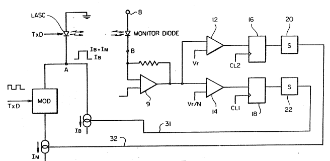
FIG 3 illustrates a schematic illustration of one preferred
embodiment of ~e invention. Referring to dlis figu~e, laser diode
LASC to be controlled has its anode connected to junction A which in
30 tum is connected in parallel to first and second current sources IM and
IB~ The laser diode anode is connected to the current source IM ~ -
~rough a switch MOD having a data input TxD which completes a pa~
between the anode and the current source IM On1Y during HIGH output
frame periods of dle laser~ Light emitted by dle laser diode is
3s monitored, preferably via a back facet of ~e laser diode, by a monitor
~ Z~
2~2~323
~W ~ 93/13577 7 PC~r/US92/11157
diode connected to a bias voltage 8. A current output of an anode B of
the monitor diode is converted to a voltage by a transimpedance
ampli~ler 9 which is connected to first and second control circuits 32,
31. Each control circuit includes a comparator 12, 14, a ~lip-flop 16,
s 18, having clock inputs CL2 and CLl respectively, and a current
integrator 20, 22. The control loop 31 is connected to the constant
current source IB. and the control loop 32 is connected to the other
constant culTent source IM-
In operation, during the LOW training pulse, switch MOD is
open so anode A is connected to only the pedestal current source IB.
Current from the laser output anode B is converted to a voltage by the
amplifiler 9 and presented to the comparator 14. Upon being strobed by
CLl by the flip-flop 18, the comparator puts out a HIGH or LOW pulse
15 depending on whether or not the amplifier voltage is above or below the
threshold V R/N- This pulse is utilize by the integrator 22 to either
decrease or increase a value of IB SO as to maintain the LOW power
output of the laser constant and ~oggling about dle dynamic re~rence
established by VR/N.
During ~e HIGH training pulse, switch MOD is closed so that ~e
laser LASC anode A is cor~nected to bodh ~he cursent source IM and IB. ` ~`
An output of the laser L ASC is monitored by dle monitor diode, and a ~ ~:
current ~rom its anode B is again converted to a vol~age by the
2s amplifiler 9 and presented to dle comparators 12, 14. Upon b~irlg
strobed by CL2, the flip-flop 16 causes dle voltage at comparator 12 ~o
be compared to the predetermined HIGH reference voltage V R. and the i
resultant compar~son is inputted to d~e integrator 20 to adjust IM UP or
dowrl to keep dle HIGH laser outpu~ toggling about its reference value. : ` ,
As can be appreciated, the reference voltages V R and VR/N of the
comparators~l2, 14 readily result in a laser extinction ratio which is ~ ;
approximately equal to N.
2~2~-323
~WO 93/13577 ~ PC~/US92/~; 157
According to another aspect of the invention, the laser control
circuit of dle present invention is very easy to optimize and set prior to
being used for transmitting information. Specifically, according to the
invention, ~he reference voltages Vr and Vr/N are maintained in a fixed
ratio by being connected to a voltage divider network, i.e. a pair of
resistors in series, as is well understood in the art, and accordingly by
simply adjusting an input voltage to the ~oltage divider networ~ one can
easily adjust both ~he LOW power output and the HIGH power output of
the laser simultaneously without varying the laser extinction ratio.
0 Hence, with a single adjustment, ~e laser out~ut can be optimized so as
to achieve ~e desired ex~inction ratio N. Pnor art lasers typically
requi~e multiple adjustments for setting a bias power and a HIGH
power. An example of a preferred voltage divider network is
illustrated in FIG SB by resistors R96, R97 which form a vol~age
divider network for reference voltages inputted to comparators 12, 14.
FIG 4 shows one preferred embodiment of the switch MOD, the
switch comprising ~Irst and second ~ransistors 40, 41, a cun~nt source
IM being connected to their common anodes, and their cathodes being
2 o connected to the laser LASC being modulated, as shown. During ~ -
pe~iods of HIGH ouqput pulses for ~e laser I~SC, transistor 41 is
enabled so dlat the laser LASC is biased by dle dlreshold cutTent IB and
dle modulation cunsnt IM, and when a LOW puLse is to be genera~ed by
the laser LASC the transistor 41 is disabled so that the anod~ A of ~e
2s laser is only cormected to the pedestal current IB.
FIGs 5A and 5B illustrate a detailed prefemd electrical
~chematic of a circuit according to the invention. For ease of
illustration, elements in E~G SA and 5B which perform the functions
refer~ed to in FIG 3 are identified by identical reference symbols in
each of these figures. Refe~g to FIG 5A, since it is preferred to have
a ca~ode of the laser LASC connected to ground and since lXD data is
assumed to be received from an electrical bus at level of +SV and 0V, a
voltage converter 50 is provided ~or converting the TxD voltages from
3s +SV and 0V to 0V and -SV respectively. These converted voltages are
WO 93/13577 9 2 1 2 6 3 PClr/US92/~ 1157
then inputted to the switch MOD which selectively connects the laser
anode with the constant current IM as described during HIGH peliods.
An output B of the monitor laser is connected to the transimpedance
amplifier 9 which is then connected to first and second feedback paths
5 32, 31 each having a comparator, flip-flop, and integrator, as
previously described. Feedback loop 31 which includes the comparator
14, flip-flop 18, and integrator 22, controls the pedestal current IB. and
the comparator 12, flip-flop 16, and integrator 20 of the feedback loop
32 control the modulation current IM. AS jS evident by examining FIG
SB, N equals the resistance of R96 divided by the resistance of R97. ~ ;~
FIG 6 illustrates a preferred use for the invention, this figure
showing a host digital terminal 71 connected to a plurality of optical
network units 72 via at least one optical fiber 73 which preferably
transports bidirectional traffilc. A splitter/combiner 74 splits a signal ~ `
originating from the host digital terminal from the ~Iber 73 to a
plurality of additional fibers 75 for transmission to each optical network
unit, and conversely signals from each optical networ~c unit 72 are `
combined at the point 74 so as to be transported to the host digital
20 terminal via the fiber 73. With such an architecture, high receiYer
sensitivity ~or each optical network unit is enhanced by maintaining an
extinction ratio of a laser transmitting from ~e host digital terminal at a ; ~
relatively high level, preferably above 10. ;`
2s Though the invention has been described by reference to certain ~: :
preferred embodiments thereof, it should be understood that various
modifications can be made thereto wid~out departing from the spirit and `~
scope of the invention, and accordingly dle invention is to be limited
only by the appended claims.
3 0 : :