Note: Descriptions are shown in the official language in which they were submitted.
2 1 2 ~ 3
P21624 . 31PCT GC
1993--10--18
TECHNICAL FIELD
The present invention relates to a boost-converter with low
losses.
BACKGROUND OF THE INVENTION
so called boost-converters are norm~lly used in order to
create a higher second dc-voltage from a generated first
voltage, which second voltage is ~`ed to some kind of load.
Such a convexter normally makes use of a series connection
of an energy storing inductor and a diode connected between
an input-te~inal from the first voltage source and an
output~terminal for the second voltage. The centre-point
between the series connected components is connected to
. .. ..earth via a switching device such a transistor. ~ capacitor
. can be çonnected between the input-terminal and earth in
order to decouple current ripples on the input and to damp
radio interference to the fed power supply system. In
addition, an energy storing ~filtering) capacitor is
connected between the output~terminal and earth. Finally,
a control circuit for the switching element is arranged to
monikor the output voltage ~rom the converter and to
control the switching element so that, for example, ~he
output voltage is kept constant independent of the load and
the input voltage for a given perisd.
A simple boost-converter thus functions in the follQwing
manner. When the switch.ing element switches to non-conduct-
ing condition, the voltage at said centre point increases
to a value which exceeds the .input voltage. The diode
conducts in the forward direction and current is fed to the
- 2 ~ 3
load including the capa~i.tor at the output. Whe~ the
switching elçment therea~ter switches tG condu~ting
condition due to a sig~al fro~ the control circuit, current
from said centre point will be conducted to earth via the
switching element, whereby the voltage at the centre point
falls. The current through the switching element is, in the
first ins~ance, composed of a contribu~ion from the input,
via the inductance~ and a contribution which is in-the form
of a reverse current through the diode which ha~ not yet
been blocked. After a certain delay, the recovexy time of
the diode, the diode is blocked and the current through,
just ~s with the voltage across, the switching element
rapidly decreases.
-15 The reverse current phenomena through the diode is a
problem with this type of circuit and creat~s power 1055es
in both the diode itself and the swit,ching element. Because
of strony current spikes, radio interference ~an also
arise.
It is generally desirable to operate the device with a high
switch frequency in order to limit the inductance value and
- the physical 6ize of the inductor. If no measures were
taken to restrict the revers~ current in the diode, the
2.5 power losses would however increase with increased fre-
quency and the ef~iciency o~ the circuit would accordingly
decrease.
Higher output-voltages al50 accentuate the problem since
diodes for higher voltages yenerally have longer recovery
times.
In order to reduce the size of the reverse current, it is
previously known to place an inductor between the diode and
said centre point~
.~
,' '~
In American patent US~A-4 ~91 96S there is for example
shown a connection in a boost-conv~rter in which the
reverse current through the diode, and thereby the switch
ing element (the transistor), is restricted using a satura-
ble inductance connected in series with the diode. The
circuit also comprises means to bring the inductor ~o a
saturated condition when the transistor is switched o~f so
that low impedance is obtained for the current in the
forward direction of the diode. Using this arrangement, a
restriction of the reverse current in the diode is achieved
and thus the associated pow~r losses in the diode and
transistor when the latter is conducting.
A ~econd solution to the same problem is described in
European patent application EP-A-351 144 in which, in
addition to the saturable inductor in series with the
diode, a second inductor element is provided through which
the reverse current passes during restriction of said
current. Energy stored in the inductor element is used when
the transistor interrupts the current path to earth to
bring the inductor in series with the diode to a saturated
condition in order to conduct the current in the ~orward
direction of the diode. Using this method it is possible to
reduce the power 10~5e~ in the circuit.
SUMM~RY OF THE INVENTION
It is an object of the invention to restrict the power
losses due to the reverse current through the main di~de in
a boost-converter and thereby increase the efficiency o~
the converter. Due to the special design, the converter is
also cheap to manu~acture, comp~ct and reliable. In
addition, it is also possible to operate the converter at
higher frequencies.
- 2 l 2 ~
4 ~:~
According to the invention an inductor which can be linear ~:
is provided between said centre point and the switching
element which, in the following, is assumed to be a
transistor. The induct~r must be demagnetized every period
so that it can block the reverse current in the subsequent
period, which demagnetizing according to the invention is
carried out in a simple and effective manner. Demagnetiz-
ation takes place by means of energy transfer to a conden-
ser which, in turn, is discharged every period towards the
output-voltage. In order to overcome for certain phenomena
which arise and which will be describ~d in the following,
a zener diode is al60 included in the circuit. The inductor
is partially demagnetized towards the zener diode. -
BRIEF DESCRIPTION OF THE DRAWINGS
,
Further features, advantages and details of the invention
will be described in greater detail in the following
description of a particular embodiment described with ~ ~.
reference to the attached drawings, in which
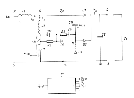
Figure 1 shows a simplified circuit diagram of the device
according to the invention.
Figure 2 shows in a nu~ber of graphs the time variance ~or
currents and voltages at several points in the circuit
according to Figure 1
DETAILED DESCRIPTION OF A PREFERRED EMBODIMENT
:
Figure 1 shows a simplified circuit diagram of the device
according to the invention. Only those components which are
important ~`or the description o the function of the
circuit according to the invention are included. Parts of
an actual circuit which are nok shown here are~ for
example, radio-interference~filters, charging circuits ~or
2126'1!~ 3
the electrolyte condensers and under voltage protection.
How these parts are arranged is evident to the skilled
person and thus do not form a part of the present inven-
tion, hence they are not hereby included.
s
An inductor L3 is provided between said centxe point and
the transistor with the purpose of re~tricting the f irst
current, i.e. the recovery current, through the diode D1
when the transistor switches to conducting condition. The
energy which i~ thereby stored in the inductance L3 is
tr~nsferred tn a condenser C18 and thereafter to the load.
The zener diode Dl9 absorbs a small portion of the anergy
from the inductance L3. ~he diode ~ shown in Fig. 1 with
dashed connections is employed in an advantageous embodi-
ment of the invention and is thus assumed in this case not
to be connected.
In greater detail, the circuit functions in the following
manner. In the initial state the transistor Ml is non-
conducting which means that the current through the
inductor L3 and the voltage acros~ the conden~er C18 are
equal to z~ro. The load current ~lows through the main
inductor L1 and the diode D1 to the load ZL.
25 . In order to control the switching element, a control
circuit 10 is provided which, in the embodiment, is in the
form of a micro-circuit with the denotation UC3854 ~rom the
company Unitrode and is provided with normal peripheral
components and voltage supply. Inpu~ signals for the
control circuit are the voltages UO~ UD~ a reference
voltage UR and a voltage which is a ~unction of the current
iL according to Figure lo The output voltage, i.e. the
control voltage itself, is denoted by U~
By means of the influence of the control voltage U~R~ the
tr~nsistor is switched to conducting condi~ion a~ ~he point
,
2 ~
in time a according to Figure 2. Since the diode D1 in this
state is conducting, the entire output voltage UO~ will ~e
present across the conductor L3~ which implies that the
current through tha conductor L3 increases according to the
expression:
di/dt = UoUr/L3~
The current through Dl in the direction towards the load
10decreases at the same rats~ When the current has dropped t~
zero ik will change direction and a reverse current through
the diode arises. The reverse current will flow for a time
equal to the recovery time T~ of the time, whereby the peek
value i, can be expressed as:
i, = di/dt * t~
When the diode Dl blocks in the reverse direction, which
occurs at the point in time b according to Figure 2, the
20induced voltage across the inductor L3 will drive a current
through the circuit consisting of the zener diode D1~, the
diode D2 and the condenser C1~, which is charged to the
voltage U0l8, the value of which is defined by:
25 U~ ~ ~ L3~C18 * i,
In Figure 2, graph F, the nega-tive current pulse through
the zener di.ode D1~ can be seen which transports the energy
from the inductor L3 to the condenser C18. A small portion
30of the energy which is stored in the inductor L3 will
obviously form losses in the diodes D19 and D2 which is why
the sign "~" (approximately equal to~ has been used in the
above equation. By ehoosing a zener voltage which i5 very
much lower than the final voltage across the condenser C18,
3~the size of the energy loss can be restricted~ It is to be
: ''.
,, j.
.
21 2~S~
noted that the top current through the inductor L3 is the
sum of i, and the current through the inductor L1, i.e. iLI.
A resistance R2 is connected in parallel with the ~ener
diode D19 and a series combination of a resistance R3 and
a capacitor C3 i~ connected in parallel with the diode D2.
These components serve to dampen resonances which arise in
the circuit, i.a. when the diode D2 i5 switched off.
The point in time c in the graph according to Figure 2
denotes when the switched on condition of the transistor M1
is terminated and the switch is in a condition (the
interval c - d) in which the current through the inductors
Ll and L3 increases linearly according to the expres~ion:
di/dt = UD / (L1 + L3 )
Note the different scales in the graphs B and E.
-. 20 When Ml is switched o~, the point in time d in Figur~ Z,
the currsnt through the inductor L3 will immediately begin
to increase the collector voltage UMI on the transistor M1
until it reaches the value UO~, cf. graph C in Figure 2.
.~ .
When the collector voltage has reached UO~ at the point in
tim~ e, the diodes D19, D2 and ~3 ~egin to conduct. A
second negative current pulse through the zener diode Dl9
is ~hown in graph F in Figure 2. The inductor L3 is now
once more demagnetized towards the condenser C18. As can be
seen in graph D in Figure 2, the voltage Uc~8 across the
condenser Cl8 does not however increase, but decreases
instead. This is because the current through the inductor
L1 di.scharges the condenser C18 with a greater current than
that with which the inductor L3 attempts to charge it up~
The energy from the inductor L3 is accordingly transported
-- 2-12~3
via the diode ~3 to the load at the converter's output
according to the principal of the invention.
When the condenser C18 has been discharged, the point in
time f in Figure 2, there remains a small quantity of
energy stored in the inductor L3. The demagnetizing can be
continued towards the zener voltage and now takes place
relatively slowly, cf. the time interval f-g in Figure 2,
graphs E and F.
~0
With lower values of current through Ll and L3, the
starting value for the current through L3 will be so small
that L3 will be totally demagneti~ed be~ore the voltage Uc~8
has reduced to zero, which is why the current i~ in the
interval f-g in Figure 2 is zero.
~he starting value for the voltage Ucl8 at the point in time
d in Figure 2, i.e. when the transistor M1 is switched off,
doe~ not depend ~n the current through L1, but inæt~ad on
the output voltage U~ which is constant, and the recovery
time of the diode D1 and the ratio between L3 and C18. This
implies that the voltage UCt8 is always the same when M1 is
switched off.
Under certain conditions transistor ~1 could be switch on
before the inductor L3 has been able to be demagnetized.
The diodes D2 and D3 would thus be conducting at the
switching on. This implies that a recov~ry current would
flow in the reverse direction through the~diodes whi~h may
cause them damage. This can be combatted by providing an
under voltage protection which, via a filter, monitors the
input voltage U~. In the exemplified control circuit, this
can be achieved via a voltage divider on leg ~0 (enable) of
the circuit.
3~
f ~
2126i~3
The condenser C18 and the inductor L3 are now fully
discharged of energy and the transistor Ml is switched off.
A switching period is complete and the circuit is ready for
the next period.
As mentioned previously in relation to Fig. 2 and the graph
F, when the transistor switches from both non-conducting to
conducting state and conducting to non-conducting state,
energy will be transferred from the inductor L3 to the
condenser C18 via the diodes D19 and D2. A certain portion
of the energy will thus be consumed in the zener diode D19
which negatively afects the efficiency of the converter.
By connectiny a diode D4 (see Fig. 1) between the return
line S-S and the point N, the energy transfer from the
inductor L3 to the condenser C18 when the transistor
switches from non-conducting to conducting state will take
place via the transistor and the diode D~. Since the
voltage drop across the conducting transistor is lower than
across the zener diode D19, the energy losses will be
reduced, with improved efficiency as a result. The energy
transfer b~tween the inductor L3 and the condenser C1~ when
the transistor switches from conducting to non-conducting
state is not af~ected by the diode D4~