Note: Descriptions are shown in the official language in which they were submitted.
212~69
.
CONTENT-ADDRESSAB~ MEMORY WITH PROGRAMMABL~ FIBLD MAS~ING
Field of the Inventio~
The present invention relates generally to
improvements in information storage, retrieval and
processing. More particularly, the present invention
relates to improvements in content-addressable memory
(CAM) used to process data packets or other information in
a digital telecommunication system.
DescriDtion of Prior Art
A content-addressable memory (CAM) is a digital
electronic memory circuit capable of storing quantities of
digital data which can be simultaneously addressed or
searched in response to an input data word. A CAM :
typically includes an array of memory cells, each memory
cell storing a single data bit. The array of cells is
usually organized into a number of rows and columns, with
each row representing a group of stored data bits, or data
words, and each column including individual stored data
bits at a particular position in each data word. A CAM
may output the a~tual data values stored in its memory
cells when addressed by an input word. In its memory cell
organization and data storage aspects, a CAM is thus
similar to a random access memory (RAM). However, unlike
a RAM, the CAM may also output a match signal indicating
whether or not a given input word matches any of the data
words stored in the entire CAM cell array. The CAM can
thus provide parallel searching of the stored data words
in each row of the array. This parallel searching
function facilitates data a storage and retrieval in a
variety of different applications.
One important application of CAM is data packet
processing in a broadband integrated services digital
network (BISDN) operating in asynchronous transfer mode
(ATM). BISDN is presently being developed to provide a
,, ~
2126~69
- 2 -
high-capacity wide-area digital network suitable for
multimedia communication. The variable high-speed data
requirements of BISDN are efficiently handled using
flexible packet processing techniques such as those
provided by an ATM communication system. Such a system
dynamically allocates data pàcket time slots to various
users to obtain maximum network capacity for variable data ~-
traffic, rather than assigning fixed time slots to
accommodate peak user data traffic as in synchronous
10 transfer mode (STM) communication. The dynamic allocation -
of available bandwidth is accomplished, in part, by
including a header in each data packet which identifies
the packet by content rather than by a fixed time slot.
The information in the header is checked against a look-up
table to determine the appropriate processing steps for
its corresponding packet. Portions of the look-up table `
may be implemented as a CAM to facilitate retrieval of
stored packet processing information.
A significant problem with existing CAM systems is -
the effect of data fields which are not needed in a
particular processing operation, commonly referred to as
"don't care" data. In general, the don't care data stored
in a CAM will slow down the process of matching an input
word with the stored data words. In one currently used
approach, the CAM includes a capability for masking
particular columns of data bits within the CAM by setting
a CAM mask register. However, this approach often uses an
external pre-processing RAM to determine, for example, if
a particular input packet header to be processed includes -
don't care values, as well as the bit positions of the
don't care values. Additional hardware and processing
steps are therefore usually required to provide such a
data bit masking function within the CAM.
Another currently used technique for handling don't
care data within a CAM is multi-step searching of the data
.~ 2l26q69
- 3 -
wcrds stored in the CAM. For example, if one or more
fields of data bits may contain don't care values in a
given application, the CAM may first be searched with one
field of data bits masked off using a data bit masking
capability and a CAM masking register, and then if no
match is found, additional searches may be performed with
other possible don't care fields masked off. Although
this approach avoids the use of an additional external
pre-processing RAM to determine which field of bits should
be masked, the number of CAM searches which must be
performed to check for matches for a given C~M input word
is increased by a factor of 2i-1 for matching an input
word divided into j fields, each of which may or may not
contain don't care values.
An alternative to masking of don't care data fields
in a CAM is to actually encode and store don't care bits
as such. This approach is known as ternary encoding, and
involves encoding three possible data states, logic 1,
logic 0, and don't care, within the stored data words.
Two data bits are therefore required to store each of
these three data states. See S. Ramirez-Chavez, "Encoding
Don't Cares in Static and Dynamic Content-Addressable
Memories", IEEE Transactions on Circuits and Systems, Vol.
39, No. 8, August 1992. Although this storage technique
may result in a decrease in the number of memory cells
required to store, for example, intervals of sequential
integers, ternary encoding will approximately double the
required memory storage capacity in many conventional CAM
applications. The larger required memory size results in
increased system cost, increased vulnerability to failure,
and larger processing overhead. Ternary encoding is
therefore generally not considered a suitable technique
for implementing telecommunication systems such as BISDN.
As is apparent from the above, a need exists for an
35 impxoved CAM which is capable of efficiently masking -
2~26~69
- 4 - :
fields of don't care data bits without using a pre- ~ -
processing RAM, without additional searching steps or .
without unduly increasing the required CAM memory -
capacity.
5 gummary of the Invention - ~ -
The present invention provides programmable data
field masking particularly well-suited for use in a : :-
content-addressable memory (CAM). A CAM in accordance:: :
with the present invention includes at least one group of
10 memory cells interconnected by a word line and a match:~ : ~
line, with each memory cell having a bit line for . .
supplying an input bit to the cell; a number of data
memory cells within the group of memory cells, divided
into data memory cell fields for storing bits of a data ~
15 word; a mask memory cell within the group of cells and :~:
connected between two of the data memory cell fields, for
storing at least one mask bit indicating the status of at :~
least one of the data memory cell fields; and a match line
detector for detecting a signal level on the match line to
determine if input data bits supplied on the bit lines of
the data memory cells match the data bits stored in the :~
data memory cells of at least one of the data memory cell
fields. The status provided may be a don't care status,
. ~.
indicating that the data contained in a particular data ~
25 field is to be masked, or ignored, in subsequent ~:-:
processing. The CAM of the present invention may include
a number of memory words, or groups of sequentially- :~
~ ~'
2126~9
-- 5
arranged memory cells, for storing a desired number of
data words.
In accordance with one aspect of the present
invention, hierarchical field masking may be provided by
dividing the data memory cells into a first and a second
memory cell field. The mask memory cell may be connected
between the first and second data memory cell fields. The
mask memory cell indicates whether or not the bits of the
data word stored in the first data memory cell field have
a don't care status. Other data words stored within the
CAM may be similarly divided into different numbers of
data fields of various sizes.
In accordance with another aspect of the present
invention, general programmable field masking is provided
such that any of the data fields within a given CAM data
word may be programmably masked regardless of whether or
not the data fields are arranged in a don't'care
hierarchy. General programmable masking is particularly
well-suited to applications in which the data fields are
not readily arranged into a hierarchy.
As a feature of the present invention, a CAM may be ~
programmed to provide data field masking without the need ,,,'
for a pre-processing RAM. Additional external hardware
and processing steps are therefore no longer re~uired to
determine if a given data word includes data bits having a
certain status, such as a don~t care status. Overall
2~ ~6~9
- 6 -
system cost, efficiency and reliability is reduced as a
result.
As another feature of the present invention,
additional searching steps are not required to implement
the programmable field masking. The given don~t care data
may be indicated and stored as such within the data word
itself by including one or more additional mask bits
within a given word. A single search of the CAM, with the
appropriate mask bits stored therein in accordance with
10 the present invention, will be sufficient to determine if - ~ -
an input word matches any of the stored words. ; ~;
As an additional feature of the present invention,
programmable field masking is provided without the need
for a significant increase in CAM memory cell capacity.
Instead of the two-fold increase in required capacity
typically associated with ternary don't care encoding,
only a small increase in CAM memory capacity is required -
to store, for example, a single mask bit to provide
hierarchical two field masking of a given data word.
As a further feature of the present invention, a ~
programmable field-masking capability will provide data -
packet processing advantages in BISDN systems using ATM
communication, as well as data storage and retrieval ;
improvements in a variety of other applications. The
programmable field masking approach provided is highly
212~4~
flexible, and does not depend upon the characteristics of
a given set of data words.
The above discussed features, as well as additional
features and advantages of the present invention, will
become more readily apparent by reference to the following
detailed description and the accompanying drawings.
Briof Descri~tion of the Drawin~
FIG. 1 illustrates an exemplary data word divlded
into several data fields.
FIG. 2 is a block diagram of an exemplary packet
switch incorporating a look-up table which may be
implemented as a CAM.
FIG. 3 is a block diagram of an exemplary data packet
processing system which utilizes a CAM to process ATM data
packet headers.
FIG. 4 illustrates an exemplary data word
corresponding to a packet header in a typical ATM
telecommunication system.
FIG. 5 illustrates an embodiment of a data word in
accordance with the present invention using the packet
header of FIG. 4 with a single mask bit between two fields
of data bits.
FIG. 6 illustrates another embodiment of a data word
in accordance with the present invention with three fields -
of data bits separated by mask bits.
:` 212~69 ':
- 8 - :
FIG. 7 is a block diagram of an exemplary memory word
within a CAM in accordance with the ~resent invention.
FIG. 8 is a block diagram of an exemplary memory word
including dual match line detectors in accordance with the
present invention.
FIG. 9(a) is a schematic diagram of an exemplary CAM
data memory cell in accordance with the present invention.
FIG. 9(b) is a schematic diagram of an exemplary CAM
mask memory cell in accordance with the present invention. -
10FIG. lO(a) is a schematic diagram of another
exemplary CAM data memory cell in accordance with the
present invention.
FIG. lO(b) is a schematic diagram of another ;~
exemplary CAM mask memory cell in accordance with the
present invention.
FIG. lO(c) is a schematic diagram of another ~
exemplary CAM mask memory cell in accordance with the ~ ;
present invention.
FIG. 11 is a block diagram of another embodiment of a
memory word utilizing multiplexed mask memory cells in
accordance with the present invention.
FIG. 12(a) is a schematic diagram of an exemplary
multiplexed mask memory cell suitable for use in the CAM
word of FIG. 11.
~,,.
' ~'
';:
212~469
g
- FIG. 12 (b) is a schematic diagram of another
exemplary multiplexed memory cell suitable for use in the
CAM word of FIG. 11.
Detailed Descri~tion
The present invention provides a programmable field
masking apparatus and method which improves the efficiency
of data storage and retrieval. Although the improvements
provided by the present invention are illustrated herein
primarily in the context of ATM data packet processing in
a telecommunication system, it should be understood that
similar improvements are provided in other CAM
applications, including, for example, searching stored
dictionaries or numerical data.
FIG. 1 shows an exemplary data word 10. The data
. . ~, .
word 10 is divided into a first data field 12, a second
data field 14, and a third data field 16. Each of the
data fields 12, 14, 16 within the data wo d 10 includes a
number of data bits. The particular arrangement of data
words and division of data words into data fields may vary
greatly depending upon the application in which the data
word is used. For example, the data fields within data
word 10 may include any number of data bits, and in
certain applications a given data field may include only a
single data bit. The data fields 12, 14, 16 may be -~
organized into a data hierarchy such that if the data bits
2 1 2 6 ~ 6 9
-- 10 --
within data field 12 have a certain status, such as a
don~t care status, the data bits within data field 14 may
or may not share that same don~t care status. However,
if the data bits within data field 14 or 16 are don~t care
S values, then the data bits within all previous fields,
such as field 12, must also be don't care values. Thus,
the fields within data word 10 are organized into a
hierarchy from right to left, with the right-most field,
field 16, having the highest priority in the hierarchy.
This means that if, for example, we ignore a given field
of a word as containing don't care values, we also -
automatically ignore any lower priority fields within the
word. Such a hierarchical arrangement of data fields is
inherent in many data communication applications, such as
a typical ATM telecommunication system.
In telecommunications systems, transmitted data
packets typically include a header which identifies the
packet. The data in the header may also be used to access
a stored look-up table to determine subsequent processing
steps required for that packet. FIG. 2 is a block diagram
of an exemplary packet switch 20 which incorporates such a
look-up table. The packet switch 20 is controlled by a
, packet switch controller 21 and supplies a plurality of
packet inputs 22 to a plurality of packet outputs 23. The
packet switch 20 also includes a look-up table 24 stored
within memory which may be a CAM, RAM, or a combination of
~ . ' ' ,.
212646~ `
11 --
CAM and R~M. The look-up table 24 is shown qualitatively
as a unconnected block within the packet switch 24, but it
should be understood that a typical packet switch will
also contain additional processing elements and
interconnections not shown in FIG. 2. The exemplary look-
up table 24 includes columns corresponding to various data
fields in a typical ATM packet header. A first column 25
contains data corresponding to a packet virtual path -
indicator (VPI), and a second column 26 contains a packet
virtual channel indicator (VCI). The VPI and VCI data are
used to determine the subsequent packet routing. A third
column 27 contains this routing (RTE) information, and a -
fourth column 28 contains any additional information
needed to process the data packets within packet switch
20. In the ATM example shown, the VPI and VCI columns 25,
26 will typically be implemented as a CAM, while the third
and fourth colu~ns may be implemented in RAM.
The headers of packets applied to packet inputs 22
are matched against the VPI and VC~ data fields stored
within columns 25, 26 in the CAM. If a match is obtained,
the match line of a particular row 29 will address the
routing and other information within columns 27, 28
! associated with that row. For example, if an incoming
packet header contains data Pl and Cl in its VPI and VCI
data fields, respectively, these fields will match with
the CAM word in row 29. The match line of this CAM word
~` 2126~9 ;:
- 12 -
will therefore address the corresponding row in the RAM,
yielding routing information Rl. The routing information
R1 may indicate that the packet switch 20 is to output a ;
data packet with data Pl and Cl in its respective VPI and
VCI fields onto a particular packet output 23 identified
as R1. The packet switch 20 thus processes information in
the headers of input data packets in order to determine
routing and other subsequent processing steps for the data
packets. The arrangement of data rows and columns within ~ ~`
look-up table 24 will, of course, vary depending upon the
application. The exemplary look-up table 24 in FIG. 2 is
simplified to illustrate the look-up mechanism, and in
reality may be considerably more complex, containing
additional information for replacing the packet headers,
15 monitoring traffic flow in the network, and the like. ;~
FIG. 3 is a block diagram of a more general
implementation of a packet processing system 30 including
a look-up table implemented with both CAM and RAM. The ~ ~
exemplary processing system 30 includes a data packet ;
input 31 which drives a pre-processor 32. The pre-
processor 32 separates the data packet header from the
other information within the packet, or packet payload,
and supplies the packet header to a CAM 33. Controller 34
regulates access of incoming packet headers to the CAM 33,
where the headers are compared to stored data words. If a
match with a particular data word stored in the CAM 33 is
-~ 2~2~469 ~ ~ :
- 13 -
found, a match line associated with that word is
triggered. The match line of each data word within the
CAM 33 corresponds to a row of memory cells within RAM 35.
When a match triggers a particular match line within the
CAM 33, the match line addresses the RAM 35 to access the
additional processing data for the input data packet. As
described above, the processing data may be routing
information and/or other types of information. The
processing information is supplied to processor 36 where
the remaining portion of the data packet, typically the
packet payload, is processed in accordance with the data
stored in RAM 35. The system 30 may therefore perform a
function similar to that provided by packet switch 20 in
FIG. 2, or may perform other types of processing. Since
lS the CAM 33 may be searched in parallel for matches with an
incoming packet header, the arrangement shown in FIG. 3
facilitates data packet processing by speeding up the
search of memory in RAM 35. The system of FIG. 3 thus
provides memory storage and retrieval advantages over a
20 RAM-based packet processing system. ~ `
The data fields in a typical ATM packet header are
shown in FIG. 4. An exemplary data word 40 includes a VPI
data field 41, a VCI data field 42, and an IF data field ~-
43. As mentioned above, the VPI and VCI data are used to `
identify subsequent processing steps for the packet. In
an ATM system, several virtual channels may be combined
:.. `.' `~
: :
' ` '~.':
"'' ~, ~',
' ~ . 2126~69 , '
- 14 - '
together within a given virtual path, and therefore an ATM
channel may be identified by its VPI alone or by both its
VPI and VCI. For channels which are only VPI-based, the
VCI data field in the packet header has a don't care
S status, and should be ignored, or masked, when matching is
attempted in the CAM. In order to handle the possible
don~t care values, many existing techniques use multi-step ~'
matching. The CAM will first be searched with both the
VPI and VCI fields, and if no match is found, then the CAM
will be searched with the VCI field masked off in order to
properly match a VPI-based channel. Since in this example
the data word is divided into two fields, two searching
steps are usually necessary using available techniques.
The present invention avoids these additional processing
15 steps by storing one or more mask bits within mask memory ~ ;
cells in each memory word in the CAM. ;~:
FIG. 5 is an exemplary data word which provides
hierarchical field masking in accordance with the present ; ~
invention. The data word 45 includes a lower data field '
46, an upper data field 47, and a mask bit 48 separating
the two flelds 46, 47. The mask bit 48 indicates the
status of the bits within the first data field 46. For ''
example, if the data field 46 contained data which had a
don't care status in a given application, the mask bit 48
is set such that the data bits within data field 46 are
ignored in CAM matching. If the mask bit 48 is set to a'~
21216~63
logic 1 value, the data bits within the lower data field
46 are used in the CAM matching process. However, if the
mask bit is set to a logic 0 value, the data bits within
the lower data field 46 are ignored as don't care values. ~ -
In either case the data bits within the upper data field
47 are used regardless of the status of the mask bit 48.
AS used herein, a logic 0 level is generally a low voltage
level which will be sufficient to turn an NMOS transistor
off, or place the transistor in a nonconductive state,
when present at the transistor gate. A logic 1 level is
generally a high voltage level sufficient to turn an NMOS :~
transistor on, or place it in a conductive state, when
present at its gate. It will be understood by those
skilled in the art that the logic levels associated herein `
with a given function may be reversed or otherwise altered
in various alternative embodiments of the present -
invention.
The exemplary data word 45 includes data fields which
correspond to those shown in FIG. 4. In an ATM
20 application, the size of the first data field 46 of data -
word 45 may be chosen to include sixteen data bits. These
sixteen bits correspond to the VCI field 42 of the
exemplary ATM data word 40 shown in FIG. 4. The second
data field 47 of data word 45 may include fourteen data
bits to store the VPI data field 41 and the IF data field
43 of ATM data word 40. In this exemplary embodiment, the
.
.. ...
;.. . . .
-:` 2~2~4~9
mask bit 48 is located between first field 46 and second
field 47. The lower field 46 thus includes VCI data which
may or may not be don't care data in a given packet. Mask
bit 48 is set to a particular value in a given packet
header to indicate that the VCI in lower data field 46 is
don't care data for that header. Since most ATM data
packets will include at least a VPI indicator, it will
generally not be necessary in such an application to mask ~ ;
the data bits in second data field 47. The ATM header
data thus has an inherent hierarchy, with the VPI data
having a higher priority than the VCI data. Although the
arrangement shown in FIG. 5 is particularly well-suited
for use in ATM communication, alternative applications may
utilize a different data field hierarchy. General ;~
masking, as opposed to hierarchical masking, which
provides the capability of masking either the first or
second data fields 46, 47, will be discussed in greater ~;
detail below.
FIG. 6 illustrates an embodiment of a data word
providing hierarchical field masking of three data fields
in accordance with the present invention. The data word
50 includes a irst data field 51, a second data field 52,
and a third data field 53. In this exemplary arrangement,
a first mask bit 54 is located between first data field 51
and second data field 52. A second mask bit 55 is located
between second data field 52 and third data field 53. The
2~26469
- 17 -
data fields 51, 52, 53 are arranged in a hierarchy such
that the don't care status of the fields 51, 52 are
indicated by the values of the mask bits 54, 55. For
example, if first mask bit 54 is a logic 0 value, it would
indicate that the data within data field 51 has a don~t
care status. Similarly, if the second mask bit 55 has a
value which is a logic 0, it would indicate that the data
fields 51 and 52 are both don't care values to be ignored
in CAM matching. If both first and second mask bits 54,
55 have logic 1 values, it would indicate that all three
data fields of the data word 50 are to be used in CAM
matching. The hierarchical field masking described above
may be readily extended to data words including any number
of data fields, with any number of data bits within each
15 field. '
FIG. 7 illustrates an exemplary CAM memory word for
use with the data word arrangement shown in FIG. 5. The
arrangement shown is particularly useful for two field
masking when the priority of the second field is greater
than that of the first field. Only a single memory word
in the CAM is shown. It should be understood, however,
that a typical CAM will include a relatively large number
of memory words similar to that shown in FIG. 7. The
memory words within the CAM will typically be arranged
.. .
vertically as rows of an array, with each row
interconnected via bit lines extending through the CAM
. . ~"
.. ...
,. :,
2:126~9
- 18 -
memory cells of each memory word. The term "memory word~
is used herein to refer to the hardware within the CAM
used to store a data word. A CAM memory word in
accordance with the present invention may therefore
include not only a group of data and mask memory cells,
but also other supporting circuitry, such as, for example,
a match line detector and a word line driver.
In the exemplary memory word 60 shown in FIG. 7, a
first data field 58 includes a plurality of CAM data
memory cells 61. Similarly, a second data field 59
includes a plurality of data memory cells 62. The first
and second data fields 58, 59 are separated by a mask
memory cell 63. The mask memory cell 63 provides the
masking function described above. A data word may be
stored in a given row of memory cells by placing a write
signal on the word line which interconnects the row of
cells, and the desired data bit on the bit line
interconnecting a column of cells. The write signal
activates an individual memory cell to accept and store
the data bit value present on its corresponding bit line.
A word line driver 64 supplies a write signal which
enables the storage of values on the bit lines of a memory
! cell. During matching, an input data word supplied on the
bit lines is compared to the data word stored within the
25 CAM word line. The CAM cells 61, 62 store the data word
for the single exemplary memory word shown. If an input
2126~69
- 19 -
data word matches the data word stored in the CAM data
memory cells, a match signal, which may be, for example, a
current or voltage level, is detected in match line -
detector 65 and supplied to match detector output 66. The
5 match detector output 66 may be used to drive a RAM to `
access additional packet processing information.
Alternatively, the match detector output 66 could be used
to set an address value in a set of programmable address
elements. Each address element is pre-encoded to be
triggered into a high or low state in response to a match
signal level, with each set of triggered elements
representing a unique address which may be used in
subsequent processing. A match signal on match detector
output 66 could also be utilized for a variety of other
purposes, as appropriate in a given application.
Both the first and second data fields 58, 59 in FIG.
7 are shown containing multiple data memory cells. ;`
However, as mentioned above, in certain applications a
particular data field may contain only one data memory ;~
cell. Although the exemplary data memory cells discussed
herein generally store a single data bit, alternative
cells could store more than one bit. The memory cells
within first and second data fields 58, 59 are referred to
herein as data memory cells because they typically contain
header data bits rather than mask bits. Although the mask
bits stored within mask memory cell 63 may also be
- 20 -
- characterized as data, the cell 63 is referred to herein
as a mask memory cell, indicating that the bit contained
therein performs a masking function. The mask bit stored
within masX memory cell 63 indicates the status of the
data bits within first data field 58. For example, if
mask cell 63 contains a logic 1 value, the data within
data field 58 is used in CAM matching operations.
However, if mask memory cell 63 contains a logic 0 value,
this indicates that data field 58 has a don't care status,
and that the bits contained therein are to be ignored, or
masked, in subsequent CAM matching. Memory word
embodiments capable of storing the exemplary three-field
data word of FIG. 6, as well as other alternative
embodiments, could also be used.
FIG. 8 shows an alternative embodiment of a CAM
memory word 60 in accordance with the present invention.
In this embodiment two match line detectors 65, 67 are
used to provide general two field masking. The CAM memory
word 60 is again divided into first and second data fields
58, 59. A single mask memory cell 63 is located between
first and second data fields 58, 59. A first match line
detector 65 is located at a right-most end of the memory
word 60. A second match line detector 67 is located at a
word line driver end of the memory word 60. In this
embodiment, either first data field 58 or second data
field 59 may be programmably masked. The match line may
-' 2l2g~6~ -:
- 21 -
- be interrupted within mask memory cell 63 as will be
described in greater detail below, and therefore each
field 58, 59 may be independently matched using a right or `~
left portion of the match line on either side of mask cell
63. Matching with the first field masked is performed by
using the first match line detector 65, while matching
with the second field masked is performed by using the
sècond match line detector 67. Additional match line
detectors may be included within the memory word to
provide field masking of three or more data fields.
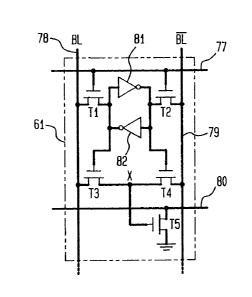
FIG. 9(a) shows an exemplary CAM data memory cell 61.
Although the data memory cell is designated by reference
number 61, it should be understood that the same memory
cell could also be used as a memory cell 62 in second data
field 59. A word line 77, a bit line 78, and a
complementary bit line 79 pass through the data memory
cell 61. A match line 80, which indicates for the entire
CAM memory word whether a particular input data word
matches the data stored in the memory word, also passes
through data memory cell 61. The word line 77 and match
line 80 extend through and interconnect the memory cells
of an entire CAM memory word, while bit lines 78, 79
èxtend through all the memory cells in corresponding bit ~ ~
positions in the other CAM memory words. As noted above, -
25 a memory word includes a group of memory cells which store ~`
a data word and any associated mask bits. The memory word
`` 2~2~69
- 22 -
is typically a sequentially-arranged group of memcry cells
interconnected by a match line and a word line, and a CAM
generally includes a large number of memory words
interconnected by bit lines.
In the exemplary data memory cell 61 of FIG. 9(a), a
single data bit is stored using the storage elements Tl,
T2, 81 and 82. The transistors Tl and T2 are typically
NMOS field effect transistors (FETs), although other types
of transistors could also be used. The gates of
transistors Tl and T2 are connected to word line 77. The
drain of transistor Tl is connected to bit line 78. The
source of transistor T2 is connected to bit line
complement 79. CMOS inverters 81, 82 are arranged in
parallel and in opposite orientations between the source
of transistor Tl and the drain of transistor T2.
Transistors Tl and T2, along with inverters 81, 82 perform
a memory storage function similar to that of a memory cell
in a RAM. Other memory storage elements could also be
used in place of Tl, T2, 81 and 82. It should be noted
that the particular designation herein of MOS transistor
terminals as source or drain is for illustration purposes
only. For example, it will be understood by those skilled
in the art that the designated sources and drains of the ` `
MOS transistors shown may be readily reversed in a manner
well known in the art to provide additional alternative
embodiments of the exemplary CAM memory cells.
"-'" 21~6~69 ~- ~
- 23 - -:
The memory storage operation in exemplary memory cell :
61 is as follows. When a write signal applied to word
line 77 is at a logic 1 level, transistors T1 and T2 are ~ ~-
turned on, supplying a data bit and its complement present
5 on bit line 78 and bit line complement 79, respectively, :
to inverters 81, 82. The parallel arrangement of
inverters 81, 82 permits the data bit to be stored within
cell 61. The inverters 81, 82 are arranged such that a
data bit supplied to these inverters when a write signal :
on word line 77 is a logic 1 will be sustained within
invertors 81, 82 even after the signal on word line 77
returns to a logic 0. The write signal applied to word ~ ;
line 77 therefore controls the data which is written into
memory cell 61 in accordance with the values present on
15 bit line 78 and bit line complement 79. Once a data bit ~
is stored within memory cell 61, the bit line 78 and bit : :
line complement 79 are no longer used to supply data to
the memory cell 61. Regardless of subsequent bit values ::-
on bit line 78 and bit line complement 79, the bit value -
20 present on these lines when word line 77 was last at a ~
logic 1 value determines the data content of the memory ~.
cell 61. Typically, the word line 77 is maintained at a
logic 0 value during a match operation. Bit line 78 and
bit line complement 79 are then used to supply a data bit
of an input data word to be checked for a match with the
data bit stored in memory cell 61. NMOS transistors T3, :.
21~6~9
- 24 -
T4 and T5 are used to implement this matching function.
Although these transistors are shown as NMOS, other types
of transistors, including PMOS, may also be used in
alternative embodiments.
In the exemplary data memory cell 61, transistor T5
sets the signal level on match line 80. Transistor T5 may
be in one of two states. When the point X, at the gate of
T5, is low, T5 is off and match line 80 is floating. When
X is high, match line 80 is pulled to ground, or a logic 0
value, via T5. The bit stored in memory cell 61 will be
present in uncomplemented form on the gate of T3, and in
complemented form on the gate of T4. If a logic 1 is
stored in cell 61, T3 is turned on, placing the current
data bit on bit line 78 at the gate of transistor of T5.
If the current value of bit line 78 is also a logic 1, T5
will turn on and pull the match line 80 to ground. If a -~
logic 0 is stored in cell 61, T3 is turned off. The gate
of T4 is supplied with a logic 1 from inverter 81 and T4
will therefore be turn~d on, placing the current value of
complementary bit line 79 at the gate of T5. If the value
present on bit line complement 79 is a logic 0, a match
has occurred and the gate of T5 is at a low value such
; that match line 80 will float. In the exemplary cell 61, ~ -
therefore, a match results if the bit line 78 has a value ~ ~-
which is the complement of the stored bit, and the bit
line complement 79 has a value which is the same as the
- 212S~9
stored bit. The sequential arrangement of data memory ~`~
cells 61 within first data field 58 will therefore provide
a NOR function. The match line 80 is pulled low unless a `
match occurs in all of the cells 61, in which case the
match line floats. The match line detector 65 detects a
change in the match line 80 signal level to indicate
whether or not a match has occurred. As noted above, the
match line signal level detected may be a current or a
voltage level. -
FIG. 9(b) is a schematic of an exemplary mask memory
cell 63 in accordance with the present invention, suitable
for use with the data memory cell 61 of FIG. 9(a). The
mask memory cell 63 also includes transistors T1, T2 and
inverters 81, 82 which operate as described above to store
a mask bit within mask memory cell 63. Word line 77 and
match line 80 pass through mask memory cell 63 as shown.
A bit line 83 and bit line complement 84 pass vertically
through cell 63 and supply a mask bit which is written
into cell 63 in a manner previously described. The match -
line 80 passing through mask memory cell 63 is divided
into a left portion 85, and a right portion 86. The left
portion 85 of match line 80 extends through the data
memory cells 61 to the left of the mask cell 63. The ~ -
right portion 86 of match line 80 extends through the data
memory cells 62 to the right of mask cell 63. The data
,~.~.,i,`, ` ,.`, ;;
-~ 2~ 2S~69
cells 61, 62 may be as shown in FIG. 9(a) when the mask
cell 63 shown in FIG. 9(b) is used.
Transistors T6 and T7 serve as a switch in series
with the match line 80 within cell 63 to effectively
interrupt the match line passing through the data memory
cells on either side of mask cell 63 in accordance with a
stored mask bit. In this embodiment, transistor T6 is a
PMOS device, while transistor T7 is an NMOS device. The
transistors T6 and T7 are therefore MOS transistors of
opposite channel type. When a logic 1 is stored in mask
memory cell 63, the gate of T6 is low and T6 is therefore
on. The drain and source of T6 are connected in series
with the match line 80 and in parallel with the drain and
source of T7. At the same time, a logic 1 is present at
the gate of T7, and T7 is therefore on. Thus, the left
portion 85 of match line 80 is connected to the right
portion 86 of the match line 80 through the drain and
source of transistors T6 and T7 such that match line 80 is
uninterrupted in passing through mask memory cell 63 and
data memory cells 61, 62 of the exemplary CAM word shown.
However, when a logic 0 mask bit is stored in the
mask memory cell 63, the gate of T6 is high, and the gate
of T7 is low, turning T6 and T7 off. The left portion 85
of match line 80 is thereby disconnected from the right
portion 86 such that transistor T5 in each of the data
memory cells 61 to the left of mask cell 63 is -~
.~.......
` . , . ~ ~ ; ' ~ ' . ,;' .'. '
2l2~ 69
disconnected from the portion of the match line 80 which
passes through data memory cells 62 to match line detector
65. Therefore, the data bits stored in data memory cells
61 are masked, or treated as don't care values, during
matching. The mask bit stored in cell 63 thus determines
the don~t care status of the first data field 58. In
altexnative embodiments of the cell 63, a single
transistor, such as either of the transistors T6 and T7
alone, could be used in place of the parallel combination
shown to effect an interruption of match line 80. The
arrangement shown in FIG. 7 may be extended to larger
numbers of data memory cell fields by separating the
additional data fields by mask cells. In the embodiment
shown, the word line driver 64 is typically adjacent a
left-most data field while match line detector 65 is
adjacent a right-most data field. -
Another exemplary CAM data memory cell 61 is shown in
. .~.
FIG. lO(a). Again; the same data memory cell may be used - ;
for memory cell 62. Word line 77 passes through data
memory cell 61, and other data and mask memory cells 61,
62, 63 in the C~M memory word 60. Word line 77 enables
data storage in the memory cells as previously described.
Transistors T3 and T4 provide a signal level at point X, ~ -
the gate of transistor T8, during matching. It should
again be noted that during matching operations in a CAM,
word line 77 will generally be disabled, or held at a
' "'~ "',` '
' ~
2~2~69
,
- 28 -
- logic low level in this case. If we assume a iogic 0 is
stored in data memory cell 61, this stored logic 0 is
present at the gate of T3 and T3 is therefore off. A
logic 1 is present on the gate of T4 and therefore T4 is
5 turned on. If, during a matching operation, a logic 0 is ~-
applied to bit line 78, and a logic 1 is applied to bit
line complement 79, the logic l on the bit line complement
79 is supplied via T4 to the gate of T8. T8 is thereby
turned on and a left portion 93 and a right portion 94 of
match line 80 passing through cell 61 are connected. This
corresponds to a match between the bit lines and the bit ~ -
value stored in the data memory cell.
If a logic 1 is stored within data memory cell 61, a
logic 1 will be present on the gate of T3, thereby turning
T3 on and connecting bit line 78 to the gate of T8.
Similarly, a logic level 0 is present at the gate of T4,
thereby turning T4 off and preventing signals from passing
from bit line complement 79 to the gate of T8. If a
signal on bit line 78 is a logic 1, corresponding to a
match with the data bit stored in cell 61, the gate of T8
will be high, connecting left portion 93 and right portion
94 of match line 80 in cell 61. If a logic 0 is present
on bit line 78, corresponding to a non-match between the
bit line and the stored data bit, the gate of T8 will be
low, thereby turning T8 off and interrupting signal flow
2~26~
- 29 -
between left portion 93 and right portion 94 of match line
80.
The match line 80 passing through the memory word 60
will be uninterrupted only if transistor T8 in each data
memory cell in memory word 60 is on. The memory cell 61
shown in FIG. lO(a) is referred to as a NAND-type memory
cell because a plurality of adjacent data memory cells
provide a NAND function. Thus the match line will be -
triggered, indicating a match between an input data word -~
and the data word stored in the CAM memory word 60, only
when all of the series transistors T8 are in an on state. - -
A single T8 in an off state will disrupt the match line 90
and provide a floating match line signal, which
corresponds to a non~match with the stored data word. ~-
FIG. lO(b) is a schematic of another exemplary mask
memory cell 63 in accordance with the present invention,
suitable use with the data memory cell 61 of FIG. lO(a).
Word line 80 passes through mask memory cell 63 and
connects the cell to the respective data memory cells 61,
62 in first and second data fields 58, 59. The storage ~
function provided by transistors Tl, T2 and inverters 81, `
82 was described previously. Bit line 83 and bit line
complement 84 are used to write a mask bit to the mask
memory cell 63. The match line 80 passing through the ;~
mask memory cell 63 includes a left portion 99 and a right
portion 100. The left portion 99 of match line 80 is
~ 212S~3
- 30 -
connected to the right portion 94 of match line 80 in a
right-most data memory cell 61 of adjacent first data
field 58. The right portion 100 of match line 80 is
connected to the left portion 93 of match line 80 passing
through a left-most data memory cell 62 of adjacent second
data field 59. Transistor T9 has a drain connected to
left portion 99 of match line 80 and a source connected to
right portion 100. The gate of T9 is connected to the
stored memory bit at the source of T1. T9 is therefore in
an on or an off state depending upon the mask bit stored
in mask memory cell 63. It should be recognized that a
parallel transistor of opposite channel type, with its
gate connected to a memory storage element storing the
complement of the mask bit, may also be included in the
embodiment of FIG. lO(b). This parallel transistor could
be connected in parallel with, for example, transistor T9,
in a manner similar to the connection of T6 and T7 in FIG.
9(b). ~ `
The complement of the stored mask bit is present at
the drain of T2 and also at the gate of T10. When the
stored mask bit is at a logic 1, T9 is in an on st~te.
The match line left and right portions 99, 100 will
therefore be connected through T9, providing a logic 1
signal level on match line 80, assuming the match line is
pre-charged to a logic 1 level prior to the matching
operation. Both the first and second data fields 58, 59
2 1 2 ~
- 31 -
are then used in matching. When a logic 0 is stored in
mask memory cell 63, T9 has a logic 0 at its gate and is
therefore in an off state. T10 has a logic 1 at its gate
and is therefore in an on state, allowing a connection of
match line right portion 100 to ground potential through
the drain and the source of T10. The source of T10 may be
connected directly to ground potential. An additional
transistor Tll may be included between the source of T10
and ground potential in order to protect T10 from
excessive current which may pass through it to ground
potential during match line pre-charge. The input 101 to
the gate of Tll may be tied to a logic low level during
pre-charging of the left and/or right portions 99, 100 of~ ~
the match line 80 in order to prevent excessive current - -
15 flow through T10. During normal matching operation, the~ i
gate input 101 of Tll is tied to a logic high level to -
connect the source of T10 to ground potential through the
drain and source of Tll. Other means may be used to
protect T10 from excessive current during pre-charge. For
20 example, the point X in one or more data memory cells 61,;
62 may be.forced to a logic 0 value in order to insure~ ~-
that all T8 transistors in the match line 80 are not
! simultaneously turned on to create excessive current flow ;~
through T10 during pre-charge.
Although the circuit implementation of FIG. 10(b)
preferably uses NMOS transistors, it should be understood
:::
2~ 2S~69
- 32 -
that other types of transistors may also be used. For
example, an implementation of the mask cell 63 using PMOS
transistors is shown in FIG. 10(c). The operation of this
device is similar to that of the NMOS mask cell, except
that a stored logic 1 mask bit will permit field masking,
rather than a logic 0 mask bit as in the cell of FIG.
9(b). Since T9 and T10 are PMOS devices, they will be
placed in an on state by a logic 0 at their respective
gates. A stored logic 0 mask bit will allow T9 to turn on
and T10 to turn off, thereby providing an uninterrupted
match line. A stored logic 1 mask bit will turn T9 off
and T10 on to mask data bits to the left of the mask
memory cell 63. In addition, when using a PMOS device for
T10, the drain and source interconnections are reversed,
and the drain of T10 is connected to a positive voltage
potential VDD rather than ground potential. The logic
.
levels applied to the gate input 101 of Tll are similarly ;~
reversed in the PMOS mask cell.
Another embodiment of a CAM memory word in accordance
with the present invention is shown in FIG. 11. Exemplary
memory word 105 includes a sequentially arranged group of
memory cells, with data memory cells divided into data
memory cell fields 108, 109, and 110. A match line 107
passes through and interconnects all of the memory cells
in the memory word 105, from the left-most data memory
cell in t~e first data field 108 to the match line
"'' ~
:
' ' ,', ~:'~
~ 21 ~ g~
- 33 -
detector after the right-most mask memory cell. The
memory word 105 includes a word line driver 111, at one
end of the memory word 105, and a match line detector 112
at an opposite end of the word 105. The data memory cell
fields 108, 109, 110 are separatèd by multiplexed mask
cells 113, 114, 115. The first multiplexed mask cell 113 `
is capable of storing two mask bits, a left mask bit and a
right mask bit. The first multiplexed cell 113 is located
between the first field of data cells 108 and a third
10 field of data cells 110. The second multiplexed mask cell .
114 is located between the second group of data memory
cells 109 and the match line detector 112. The third ;~
multiplexed mask cell 115 is located between the third
field of data memory cells 110 and the second field of :
data memory cells 109.
This exemplary arrangement allows any of the data
memory cell fields 108, 109, 110 to be programmably masked
in accordance with mask memory bits stored in multiplexed
mask cells 113, 114, 115. Thus, the data stored in the
data memory cell fields need not be arranged in a
hierarc~y of priority to provide masking. Any of the data
fields may be programmably masked independent of the -
status of the other data fields of memory word 105. In
the exemplary embodiment of FIG. 11, the status of the
respective data memory cell fields within CAM word 105 is
determined by two mask bits stored in multiplexed mask
~ 2126~9 ~ :~
- 34 -
- cells 113, 115 and a single mask bit stored in multiplexed
mask cell 114.
An exemplary multiplexed mask memory cell 115 is
shown in FIG. 12(a). The multiplexed mask memory cell 115
includes a left mask cell 118 and a right mask cell 119.
A word line 120 passes through the multiplexed mask cell ,~
115 as well as through the other data memory cells and
multiplexed mask cells within the memory word 105. The .,
left mask cell 118 includes a bit line 121 and a bit line ~'~
complement 122. The right mask cell 119 of the
multiplexed mask cell 115 includes a bit line 123 and a ~-~
bit line complement 124. The bit lines 121, 123 and bit
line complements 122, 124 provide mask bits to the
multiplexed mask memory cell 115. Again, the mask bits
are written into the mask cells by supplying the bits to
the appropriate bit lines while raising word line 120 to a
logic high level. Transistors T1 and T2 and inverters 81,
82, provi,de the memory storage function, as previously
described. The stored mask bit in the left mask cell 118 '~
20 in multiplexed cell 115 is pxesent at point X, and the ~
gate of T13. The complement of the stored bit is supplied ~':
to the gate of T14. Similarly, a stored mask bit is
present at the point Y in the right mask memory cell 119,
and at the gate of T15 with the complement of the stored ,~
25 bit at the gate of T16. ' ":
.. ~..
'' ' ~'' '~,
~' '
2l26~69
-
- 35 -
The left portion 125 of match line 107 is connected
to the drain of T13 within the left mask memory cell 118
of the multiplexed cell 115 and to the right-most data
memory cell within third data memory cell field 110.
Similarly, the right portion 126 of the match line 107 :~
passing through multiplexed cell 115 is connected to the
left-most data memory cell within data field 109. The
match line 107 with match line left portion 125 and match
line right portion 126 provides a match line function
10 similar to that described above in conjunction with FIGS. :
9 and 10. A bypass line 127 is included in both the left
mask memory cell 118 and the right mask memory cell 119. ~ ~ -
The bypass lines 127, 128 do not pass through the data :~
memory cell fields 108, 109, 100, but are instead used to -: ~
interconnect the multiplexed mask memory cells 113, 114, ::
115. The left mask memory cell 118 includes match line
left portion 125 and a left bypass line 127. The right
mask memory cell 119 includes match line right portion 126
and a right bypass line 128. The bypass lines 127, 128
are used to bypass, or mask, a particular data memory cell
field located between a pair of multiplexed mask cells
when the data field has, for example, a don't care status.
The mask bits stored in a particular multiplexed mask
memory ceIl will determine whether the left and right
portions of the match line are connected to allow the
2126469
- 36 -
match line to pass uninterrupted through the multiplexed
cell.
A logic 1 mask bit stored in the left mask memory
cell 118 will place a logic 1 level at the gate of T13 and
a logic 0 at the gate of T14, turning T13 on and T14 off.
This will allow match line 107 to pass through left mask
memory cell 118 and will also disconnect the bypass line
127 from the match line left portion 125. Similarly, a
logic 1 stored in the right mask memory cell 119 will
place a logic 1 at the gate of T15 and a logic 0 at the
gate of T16, turning T15 on and T16 off. This will allow -~
the right portion 126 of the match line 107 to pass
through the right mask memory cell 119, and will ;
disconnect the bypass line 128 from match line right
15 portion 126. Thus, when storing a logic 1 mask bit in -~
either the left or right mask memory cells 118, 119, an
indication is provided that an adjacent data memory cell
field does not have a don't care status and should ~ ;
therefore not be masked.
In order to mask a particular data memory cell field
within the memory word 105, one could store a logic 0 in
the mask memory cells on both sides of a data memory cell
field. By storing a logic 0 into the left and right mask
memory cells surrounding a data memory cell field, the
match line 107 is interrupted in the multiplexed mask
memory cell at both ends of the data memory cell field and
-`-` 6~ ~9 `~
- 37 -
the bypass line that connects the right and left match
line portions of the multiplexed cells at either end is
connected to bypass the data memory cell field. Any of
the data memory cell fields 108, 109, 110 may be
programmably bypassed, or masked, as having don~t care
status using the multiplexed mask memory cells shown.
An exemplary embodiment of the left-most multiplexed
mask memory cell 113 is shown in FIG. 12(b). The left-
most multiplexer cell 113 has a slightly different ~`
configuration than the third multiplexer cell 115 shown inFIG. 12(a). The exemplary multiplexed cell 113 includes a
left mask memory cell 131, and a right mask memory cell
132. Left mask cell 131 includes a bit line 141 and a bit
line complement 142, while right mask cell 132 includes a
bit line 143 and a bit line complement 144. Match line
107 within cell 113 includes a left portion 145 and a
right portion 146. A right bypass line 148 may be
connected to, for example, left bypass line 127 in
multiplexed cell 115. The operation of the right mask
memory cell 132 is the same as that of right mask memory
cell 119 discussed above. Left mask memory cell 131,
however, no longer includes a left bypass line, such as
bypass line 127 in cell 118, because there are no other
multiplexed mask memory cells to the left of multiplexed
cell 113 to connect with cell 113 to bypass a data cell
field. The single data cell field 108 to the left of
212~469
,~ -
- 38 -
left-most multiplexed cell 113 is bypassed by simply
disconnecting left portion 145 of match line 107 via
transistor T13.
In left mask cell 131, the source of T14 may be
connected to ground potential via T17. T17 may be used to
break a possible high-current path to ground during pre-
charge of the match line 107. T17 is placed in an off
state during pre-charge of match line 107, disconnecting
the source of T1~ from ground, by supplying a logic 0
signal to T17 gate input 133. T17 is then placed into an
on state during normal CAM matching operation by placing a
logic 1 signal at the gate input 133 of T17. AS mentione~
above, it may not be necessary to include a transistor
such as T17 when other means are used to prevent excess
current flow through the match line during pre-charge.
Because the multiplexer 113 is the left-most
multiplexer within memory word 105, a bypass line is not
carried any further to the left in the embodiment shown.
The bypass line may instead be terminated to ground
20 potential via T14 as discussed above. The first data ~ -
memory cell field 108 will be bypassed, or treated as
having don't care status, by simply turning off T13 in the
left mask memory cell 131 to disconnect match line left
portion 145 from the remainder of match line 107. The
right bypass line 148 in the right mask memory cell 132
may be connected to the left bypass line 127 in left mask
~-`` 21 ~6469
- 39 -
memory cell 118 of multiplexed cell 115 to effectively
bypass, or mask, the data memory cells within data memory
cell 110. The right-most multiplexed mask memory cell 114
need not include a right mask memory cell. Multiplexed
S cell 114 will therefore typically have only a single mask
memory cell storing a single mask bit. The single mask
memory cell could be, for example, the same as left mask
memory cell 118 in FIG. 12(a). Since there are no
additional data memory cell fields located to the right of
right-most multiplexed cell 114, a right mask memory cell
is not used in multiplexed cell 114.
The match line detector 112 will detect a match by
sensing the signal level of the match line 107 passing
through the multiplexed mask cells 113, 114, 115 and the
data memory cell fields 108, 109, 110. Any field of data
memory cells may be programmably masked by supplying the
appropriate mask bit or bits to the appropriate
multiplexad mask memory cell as described above. This
embodiment of the present invention thus provides general
~0 multi-field masking. Any data memory field within a given ~-
data word may be programmably masked to permit single-step
match searching of memory words in a CAM. This embodiment
i~s particularly useful in applications in which the data -
word does not have a hierarchy of don't care priorities.
When the data word does include an internal hierarchy of
data field priorities, it may be more advantageous to use
6 4 6 9
- 40 -
the embodiments described above in connection with FIGS. 7
and 8 in order to minimize the number of mask memory cells
in the CAM. ~ -
Although the foregoing detailed description has
5 described the present invention primarily in terms of a :
particular application of field masking in content-
addressable memory, it should be understood that the :
embodiments discussed are exemplary only. Many variations
may be made in the arrangements shown, including the
number and size of the data fields stored within a CAM
memory word, the number of mask bits used to mask a
particular field or fields, and the particular
implementation and interconnection of the mask memory and
data memory cells: These and other alternatives and .
15 variations will be readily apparent to those skilled in : .
the art, and the present invention is therefore limited :
only by the appended claims. ~ -~