Note: Descriptions are shown in the official language in which they were submitted.
CFO 10107 ~
_ 1 _
1 ELECTRON BEAM APPARATUS AND IMAGE-FORMING APPARATUS
BACKGROUND OF THE INVENTION
Field of the Invention
The present invention relates to an electron
beam apparatus and an image-forming apparatus, such
as a display device, in which the electron beam
apparatus is employed.
Related Background Art
Heretofore, two types of electron-emitting
devices are known; i.e., a thermal electron source
and a cold cathode electron source. Cold cathode
electron sources include electron-emitting devices
of field emission type (hereinafter abbreviated to
FE type), metal/insulating layer/metal type (hereinafter
abbreviated to MIM type), and surface conduction type
(hereinafter abbreviated to SCE), etc.
Examples of FE type devices are described in,
e.g., W.P. Dyke & W.W. Dolan, "Field emission", Advance
in Electron Physics, 8, 89 (1956) and C.A. Spindt,
"PHYSICAL Properties of thin-film field emission
cathodes with molybdenium cones", J. Appl. Phys., 47,
5248 (1976).
One example of MIHi ty~ae devicea is described
in, e.g., C.A. Mead, "The tunnel-emission amplifier",
J. Appl. Phys., 32, 646 (1961).
One example of surface conduction
'~~.2~~'~~
- 2 -
1 electron-emitting devices is described in, e.g., M.I.
Elinson, Radio Eng. Electron Phys., 10, (1965).
A surface conduction electron-emitting device
utilizes a phenomenon that when a thin film having
a small area is formed on a substrate and a current
is supplied to flow parallel to the film surface,
electrons are emitted therefrom. As to such a surface
conduction electron-emitting device, there have been
reported, for example, one using a thin film of Sn02
by Elinson as cited above, one using an Au thin film
[G. Ditter: "Thin Solid Films", 9, 317 (1972 ) , one
using a thin film of In203/Sn02 [M. Hartwell and C.G.
Fonstad: "IEEE Trans. ED Conf.", 519 (1975)], and one
using a carbon thin film [Hisashi Araki et. al.:
"Vacuum", Vol. 26, No. 1, p. 22 (1983)].
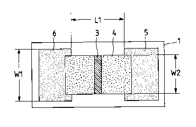
As a typical configuration of those surface
conduction electron-emitting devices, Fig. 25 shows
the device configuration proposed by M. Hartwell in
the above-cited paper. In Fig. 25, denoted by reference
numeral 1 is an insulating substrate. 2 is a thin
film for forming an electron-emitting region which
comprises, e.g., a metal oxide thin film formed by
sputtering into an H-shaped pattern. An electron-
emitting region 3 is formed by the energizing process,
i.e. flowing an electrical current, called forming
(described later). 4 will be here referred to as a
thin film including the electron-emitting region. The
- 21~6~
1. dimensions indicated by L1 and W in the drawing are
set to 0.5 - 1 mm and 0.1 mm, respectively. The
electron-emitting region 3 is shown schematically
because its position and shape are not certain.
In those surface conduction electron-emitting
devices, it has heretofore been general that the
electron-emitting region forming thin film 2 is
subjected to the energizing process called forming
in advance to form the electron-emitting region 3
before starting emission of electrons. The term
"forming" means the process of applying a DC voltage
or a voltage rising very slowly at a rate of, for
example, 1 V/minute, across the electron-emitting
region forming thin film 2 to locally destroy, deform
or denature it to thereby form the electron-emitting
region 3 which has been transformed into an electrically
high-resistance state. The electron-emitting region
3 emits electrons from the vicinity of a crack
generated in a portion of the electron-emitting region
forming thin film 2.
The electron-emitting region forming thin film
2 including the electron-emitting region 3 which has
been formed by the forming process will be here referred
to as the thin film 4 including electron-emitting
region. In the surface conduction electron-emitting
device after the forming process, a voltage is applied
to the electron-emitting region including thin film
- 4 - 212~~~5
1 4 to supply the device with a current, whereupon
electrons are emitted from the electron-emitting region
3.
The above surface conduction electron-emitting
device is simple in structure and easy to manufacture,
and hence has an advantage that a number of devices
can be formed into an array having a large area.
Therefore, various applications making use of such
an advantage have been studied. Examples of the
applications are an electron beam apparatus, e.g.,
a charged beam source and an electron beam machining
apparatus, and a display device.
As an example in which a number of surface
conduction electron-emitting devices are formed into
an array, there is an electron source wherein surface
conduction electron-emitting devices are arranged in
parallel, both ends of the devices are interconnected
by respective leads to form one row of an array, and
a number of rows are arranged to form the array. (See,
e.g., Japanese Patent Application Laid-Open No. 64-
31332). In the field of image-forming apparatus such
as image display devices, particularly, flat type
display devices using liquid crystals have recently
become popular instead of CRTs, but they are not of
an emission type and have a problem of requiring
backlights or the like. Development of self-luminous
display devices have therefore been desired. An
- 5 - 2~~s~~~
1 image-forming apparatus in which an electron source
having an array of numerous surface conduction electron-
emitting devices and a fluorescent substance radiating
visible light upon impingement of electrons emitted
from the electron source are combined with each other
to form a display device, is a self-luminous one which
is relatively easy to manufacture and has good display
quality while giving a large screen size. (See, e.g.,
USP No. 5,066,883).
In the conventional electron source comprising
numerous surface conduction electron-emitting devices,
desired one of the devices, which is to emit electrons
for causing the fluorescent substance to radiate light,
is selected by combination of wirings (referred to
as row-direction wirings) which interconnect both ends
of the numerous surface conduction electron-emitting
devices arranged in parallel, control electrodes (called
grids) which are disposed in a space between the
electron source and the fluorescent substance to lie
in a direction (called a column direction) perpendicular
to the row-direction wirings, and an appropriate drive
signal applied to the row-direction wirings and the
grids. (See, e.g., Japanese Patent Application Laid-
Open No. 1-283749).
The electron-emitting devices are handled under
a vacuum, but details of an electron-emitting charac-
teristic of the surface conduction electron-emitting
- 6 -
2ms~~~
1 device under a vacuum are yet scarcely clear.
A description will now be made of problems
caused in the conventional surface conduction electron-
emitting devices as described above and the image-
s forming apparatus, etc. employing those devices.
Problem 1
If the conventional electron-emitting device
is left not driven in an image-forming apparatus or
an enclosure for maintaining a vacuum therein, an
electrical characteristic (current - voltage) of the
electron-emitting device is changed and an emission
current from the device is increased temporarily. A
change rate of the emission current depends on the
period of time during which the device is left not
driven (i.e., standing time), the vacuum atmosphere
(degree of vacuum and kinds of residual gases), the
driving voltage and so on.
Problem 2
In the conventional electron-emitting device,
if a pulse width of the voltage applied to the device
is changed, an emission current is varied and, therefore,
it is difficult to control the amount of electrons
emitted with the pulse width.
Problem 3
In the conventional electron-emitting device,
if a value of the voltage applied to the device is
changed, its electrical characteristic is varied and
- ' - 21~~~'~~
1 an emission current is also varied correspondingly.
It is therefore difficult to control the amount of
electrons emitted with the voltage value.
Problem 4
When the conventional electron-emitting device
having Problem 1 is employed in an image-forming
apparatus, contrast and sharpness of the formed image
are lowered because of a change in the intensity of
electron beam. Particularly, when the formed image
is a fluorescent image, brightness and color of the
fluorescent image are varied.
Problem 5
When the conventional electron-emitting device
having Problems 2 and 3 are employed in an image-forming
apparatus, a difficulty in control of the intensity
of electron beam with the voltage or the pulse width
thereof applied to the device makes it difficult to
achieve gradation control of the formed image.
Particularly, when the formed image is a fluorescent
image, it is difficult to control brightness and color
of the fluorescent image.
In view of the problems as described above,
an object of the present invention is to provide an
electron-emitting device and an electron beam generator
in which an emission current is stable with a very
small change in the amount of electrons emitted
depending on the period of time during which the device
- 2126~~~
1 is left not driven (i.e., standing time) and the vacuum
atmosphere. Another object of the present invention
is to provide an image-forming apparatus which can
produce a sharp image with high contrast, in particular,
an image-forming apparatus which can form a luminous
image with a small change in brightness. Still another
object of the present invention is to provide an
image-forming apparatus which is easy to carry out
gradation control, in particular, an image-forming
apparatus which is easy to control brightness and color
of a luminous image.
SUMMARY OF THE INVENTION
The above objects are achieved by the present
invention summarized below.
With one aspect of the invention, there is
provided an electron beam apparatus comprising an
enclosure in which an electron-emitting device having
an electron-emitting region between opposite electrodes
is disposed, wherein the electron-emitting device
exhibits such a characteristic as that an emission
current is uniquely determined with respect to a device
voltage.
With another aspect of the invention, there
is provided an electron beam apparatus comprising an
enclosure in which an electron-emitting device having
an electron-emitting region between opposite electrodes
- 2126~~~'
1 is disposed, wherein the interior of the enclosure
is maintained under an atmosphere effective to prevent
structural changes of the electron-emitting device.
With still another aspect of the invention,
there is provided an image-forming apparatus comprising
an enclosure in which an electron source and an image-
forming member are disposed, the apparatus producing
an image in response to an input signal, wherein the
electron source comprises an electron-emitting device
having an electron-emitting region between opposite
electrodes, the electron-emitting device exhibiting
such a characteristic as that an emission current is
uniquely determined with respect to a device voltage.
With yet another aspect of the invention, there
is provided an image-forming apparatus comprising an
enclosure in which an electron source and an image-
forming member are disposed, the apparatus producing
an image in response to an input signal, wherein the
electron source comprises an electron-emitting device
having an electron-emitting region between opposite
electrodes, and the interior of the enclosure is
maintained under an atmosphere effective to prevent
structural changes of the electron-emitting device.
BRIEF DESCRIPTION OF THE DRAWINGS
Figs. lA and 1B are schematic views of a planar
type surface conduction electron-emitting device
- 10 -
2126~3~
1 according to an embodiment of the present invention
and Examples 1 to 3.
Figs. 2A to 2C are sectional views showing
successive steps of a process of manufacturing the
surface conduction electron-emitting device according
to the embodiment of the present invention and Examples
1 to 3.
Fig. 3 is a schematic view of a measuring
apparatus for use in the present invention.
Figs. 4A and 4B are charts showing forming
waveforms.
Fig. 5 is a graph showing dependency of a device
current and an emission current upon an activating
process time.
Fig. 6 is a schematic view of a vertical type
surface conduction electron-emitting device according
to an embodiment of the present invention.
Fig. 7 is a graph showing typical I-V charac-
teristics under a vacuum at degree of about 1 x 10⁻⁶
Torr.
Fig. 8 is a graph showing a characteristic
of emission current versus device voltage (I-V
characteristic) in the surface conduction electron-
emitting device according to the present invention.
Fig. 9 is a schematic view of an electron
source substrate, the view showing a simple matrix
array according to an embodiment of the present
11 2126~~~
1 invention and Example 4.
Fig. 10 is a schematic view of an image-forming
apparatus according to an embodiment of the present
invention and Example 4.
Figs. 11A and 11B are explanatory views of
fluorescent films in the image-forming apparatus
according to the embodiment of the present invention
and Example 4.
Fig. 12 is a schematic plan view showing the
electron source substrate according to Example 4.
Fig. 13 is a sectional view taken along line
A - A' in the schematic plan view showing the electron
source substrate according to Example 4.
Figs. 14A to 14D and 15E to 15H are sectional
views showing successive steps of a process of
manufacturing the electron source substrate according
to Example 4.
Fig. 16 is a block diagram of a display device
according to Example 5.
Figs. 17 and 18 are schematic views showing
of an electron source substrate for use in an image-
forming apparatus according to Example 6.
Figs. 19 and 22 are perspective views of panel
constructions of the image-forming apparatus according
to Example 6.
Figs. 20 and 23 are block diagrams of electrical
circuits for driving the image-forming apparatus
- 12 -
2126~~5
1 according to Example 6.
Figs. 21A to 21F and 24A to 24I are timing
charts for explaining operation of the image-forming
apparatus according to Example 6.
Fig. 25 is a schematic view of a conventional
surface conduction electron-emitting device.
Fig. 26 is a graph showing variations in an
emission current depending upon a standing time in
the conventional surface conduction electron-emitting
device.
Fig. 27 is a graph showing variations in an
emission current depending upon a pulse width in the
conventional surface conduction electron-emitting device.
Fig. 28 is a graph showing a characteristic
of emission current versus device voltage (i.e.,
variations in an emission current depending upon a
device voltage) in the conventional surface conduction
electron-emitting device.
DETAILED DESCRIPTION OF THE PREFERRED EMBODIMENTS
As a result of intensive studies for long years,
the inventors have accomplished the present invention
based on findings that an emission current and a device
current are changed mainly due to variations in the
mount of organic materials present on the surface
of a surface conduction electron-emitting device and
- 13 -
1 in a vacuum atmosphere around the device, and that
a stable electron-emitting characteristic is obtained
without variations in the emission current and the
device current by reducing a partial pressure of
carbon compounds, particularly organic materials, to
be as low as possible.
Preferred embodiments of the present invention
will be illustrated below.
The present invention concerns with a novel
structure and manufacture process of a surface conduc-
tion electron-emitting device, an electron source and
an image-forming apparatus using the surface conduction
electron-emitting device, as well as applications of
the electron source and the image-forming apparatus.
A basic structure of the surface conduction
electron-emitting devices is divided into the planar
type and the vertical type.
Figs. lA and 1B are a plan and sectional view,
respectively, showing a basic structure of the surface
conduction electron-emitting device according to the
present invention. A description will now be made
of the basic structure of the device according to the
present invention.
In Figs. lA and 1B, denoted by reference
numeral 1 is a substrate, 5 and 6 are device electrodes,
4 is an electron-emitting region including thin film,
and 3 is an electron-emitting region.
- 14 -
2126'~~5
1 The substrate 1 may be of, for example, a glass
substrate made of, e.g., quartz glass, glass having
a reduced content of impurities such as Na, soda lime
glass and soda lime glass having Si02 laminated thereon
S by sputtering, or a ceramic substrate made of, e.g.,
alumina.
The device electrodes 5, 6 arranged in opposite
relation may be made of any material which has
conductivity. Examples of electrode materials are
metals such as Ni, Cr, Au, Mo, W, Pt, Ti, A1, Cu and
Pd or alloys thereof, printed conductors comprising
metals such as Pd, Ag, Au, Ru02 and Pd-Ag or oxides
thereof, glass, etc., transparent conductors such as
In203-Sn02; and semiconductors such as polysilicon.
The distance L1 between the device electrodes
is in the range of several hundreds angstroms to several
hundreds microns, and is set depending on the photo-
lithography technique as the basis for a manufacture
process of the device electrodes, i.e., performance
of an exposure machine and an etching method, and device
factors such as the voltage applied between the device
electrodes and the intensity of an electric field
capable of emitting electrons. Preferably, the distance
Ll is in the range of several microns to several tens
microns.
The length W1 and the film thickness d of the
device electrodes 5, 6 are appropriately designed in
- 15 -
2~'~~5~5
1 consideration of the resistance values of the electrodes,
connection to X- and Y-direction wirings as mentioned
before, the problem in the arrangement of numerous
devices making up an entire electron source, etc.
Usually, the length W1 of the device electrodes is
in the range of several microns to several hundreds
microns, and the film thickness d of the device
electrodes 5, 6 is in the range of several hundreds
angstroms to several microns.
The thin film 4 including electron-emitting region
including which is positioned above and between the
device electrodes 5, 6 disposed on the substrate 1
in opposite relation includes the electron-emitting
region 3. The thin film 4 including electron-emitting
region is not limited to the structure shown in Fig.
1B, and may not be positioned over both the device
electrodes 5, 6. This case is resulted when the
electron-emitting region forming thin film 2 and the
opposite device electrodes 5, 6 are laminated on the
insulating substrate 1 in this order. Alternatively,
the entire region between the opposite device electrodes
5, 6 may function as the electron-emitting region
depending on the manufacture process. The thin film
4 including electron-emitting region has a thickness
preferably in the range of several angstroms to several
thousands angstroms, more preferably 10 angstroms to
500 angstroms. The film thickness is appropriately
- 16 -
1 set in consideration of the step coverage over the
device electrodes 5, 6, the resistance values between
the electron-emitting region 3 and the device electrodes
5, 6, the grain size of conductive fine particles in
the electron-emitting region 3, conditions of the
energizing process (described later), etc. The thin
film 4 including electron-emitting region has a sheet
resistance value of 103 to 10~ ohms/.
Specific examples of materials of the thin
film 4 including electron-emitting region are metals
such as Pd, Ru, Ag, Au, Ti, In, Cu, Cr, Fe, Zn, Sn,
Ta, W and Pb, oxides such as PdO, Sn02, In203, PbO,
Sb203, borides such as HfB2, ZrB2, LaB6, CeB6, YB4
and GdB4, carbides such as TiC, ZrC, HfC, TaC, SiC
and WC, nitrides such as TiN, ZrN and HfN, semicon-
ductors such as Si and Ge, carbon, AgMg, and NiCu.
The thin film 4 is preferably a fine particle film
in order to provide a good electron emission
characteristic.
The term "fine particle film" used herein means
a film comprising a number of fine particles aggregated
together, and includes films having microstructures
in which fine particles are not only individually
dispersed, but also adjacent to or overlapped with
each other (including an island state). The grain
size of the fine particles is in the range of several
angstroms to several thousands angstroms, preferably
- 17 -
1 10 angstroms to 200 angstroms.
The electron-emitting region 3 is made up of
a number of conductive fine particles having the grain
size preferably in the range of several angstroms to
several thousands angstroms, more preferably 10
angstroms to 500 angstroms. The thickness of the
electron-emitting region 3 depends on the thickness
of the thin film 4 including electron-emitting region
and the manufacture process including conditions of
the energizing process (described later), and is set
in an appropriate range. Materials of the electron-
emitting region 3 are the same as a part or all of
the materials of the thin film 4 including electron-
emitting region for respective constituent elements
of the latter.
A description will now be made of a vertical
type surface conduction electron-emitting device as
the other type of the surface conduction electron-
emitting device of the present invention. Fig. 6 is
a schematic view showing a basic structure of the
vertical type surface conduction electron-emitting
device according to the present invention.
In Fig. 6, the substrate l, the device
electrodes 5, 6, the thin film 4 including
electron-emitting region including and the
electron-emitting region 3 are each made of the
same materials as used for the planar type surface
18
1 conduction electron-emitting devices described above.
A step-forming section 21 is formed of an insulating
material such as Si02 by vacuum evaporation, printing,
sputtering or the like. The thickness of the step-
s forming section 21 corresponds to the distance L1
between the device electrodes of the planar type
surface conduction electron-emitting devices described
above. Depending on the manufacture process of the
step-forming section, the voltage applied between the
device electrodes, and the intensity of an electric
field capable of emitting electrons, the thickness
of the step-forming section 21 is usually set to be
in the range of several tens nanometers to several
tens microns, preferably several tens nanometers to
several microns.
Since the thin film 4 including electron-
emitting region is formed after fabricating the device
electrodes 5, 6 and the step-forming section 21, the
thin film 4 is laminated on the device electrodes 5,
6. While the electron-emitting region 3 is shown as
being linear in Fig. 6, the shape and position of the
region 3 are not limited to the illustrated ones and
depend on the manufacture conditions, the energizing
conditions in the forming process, etc.
While the electron-emitting device containing
the electron-emitting region can be manufactured in
various ways, one example of the manufacture process
- 19 - 2~~~~~~
1 is shown in Figs. 2A to 2C. Note that reference numeral 2
in Fig. 2B denotes an electron-emitting region forming
thin formed of a fine particle film, for example.
The manufacture process will be described below
in sequence with reference to Figs. lA to 2C.
1) The insulating substrate 1 is sufficiently
washed with a detergent, pure water and an organic
solvent. A device electrode material is then deposited
on the substrate 1 by vacuum evaporation, sputtering
or any other suitable method. The device electrodes
5, 6 are then formed on the surface of the insulating
substrate 1 by the photolithography technique (Fig.
2A).
2) Between the device electrodes 5, 6 provided
on the insulating substrate 1, an organic metal thin
film is formed by coating an organic metal solution
over the insulating substrate 1 formed with the device
electrodes 5, 6 and then leaving the coating to stand
as it is. The organic metal solution is a solution
of an organic compound containing, as a primary element,
any of the above-cited metals such as Pd, Ru, Ag, Au,
Ti, In, Cu, Cr, Fe, Zn, Sn, Ta, W and Pb. After that,
the organic metal thin film is heated for baking and
patterned by lift-off or etching to thereby form the
electron-emitting region forming thin film 2 (Fig.
2B). While the organic metal thin film is formed by
coating the organic metal solution herein, the forming
2126~~~
- 20 -
1 method is not limited to the coating, and the organic
metal thin film may be formed by any of other methods
such as vacuum evaporation, sputtering, chemical
vapor-phase deposition, dispersion coating, dipping
and spinning.
3) Subsequently, the energizing process called
forming is carried out by applying a pulse-like voltage
between the device electrode 5 and 6 from a power supply
(not shown). The electron-emitting region-forming
thin film 2 is thereby locally changed in its structure
so as to form the electron-emitting region 3 (Fig.
2C). A portion of the electron-emitting region forming
thin film 2 where the structure is locally destroyed,
deformed or denatured by the energizing process will
be referred to as the electron-emitting region 3. As
previously described, the inventors have found by
observing the electron-emitting region 3 that the region
3 is made up of conductive fine particles.
Electrical processes such as the forming
operation or the activation operation are carried out
in a measuring (evaluating) apparatus shown in Fig.
3. The measuring apparatus will be described below.
Fig. 3 is a schematic view of the measuring
apparatus for measuring electron emission character-
istics of the device constructed as shown in Figs. lA and 1B.
In Fig. 3, denoted by 1 is a substrate, 5 and 6 are
device electrodes, 4 is a thin film including
- 21 -
1 electron-emitting region, and 3 is an electron-emitting
region. Further, 31 is a power supply for applying
a device voltage Vf to the device, 30 is an ammeter
for measuring a device current If flowing through the
thin film 4 including electron-emitting region between
the device electrodes 5 and 6, 34 is an anode electrode
for capturing an emission current Ie emitted from the
electron-emitting region 3 of the device, 33. is a high-
voltage power supply for applying a voltage to the
anode electrode 34, and 32 is an ammeter for measuring
the emission current Ie emitted from the electron-
emitting region 3 of the device.
For measuring the device current If and the
emission current Ie of the electron-emitting device,
the power supply 31 and the ammeter 30 are connected
to the device electrodes 5, 6, and the anode electrode
34 connected to the power supply 33 and the ammeter
32 is disposed above the electron-emitting device.
The electron-emitting device and the anode electrode
34 are disposed in a vacuum apparatus which is provided
with additional necessary units (not shown) such as
an evacuation pump and a vacuum gauge, so that the
device is measured and evaluated under a desired vacuum.
The evacuation pump includes a normal high vacuum
apparatus system comprising a turbo pump and a rotary
pump, and a ultra-high vacuum apparatus system compris-
ing a sorption pump and an ion pump that employs no
22
1 oil for evacuation, these two systems being selectively
switched over. Further, a quadruple mass spectrometer
(not shown) is installed for measuring residual gas
in the vacuum apparatus. The entire vacuum apparatus
and the electron source substrate can be heated up
to 200°C by a heater (not shown).
The measurement is usually performed by setting
the voltage applied to the anode electrode to be in
the range of 1 kV to 10 kV, and the distance H between
1G the anode electrode and the electron-emitting device
to be in the range of 2 mm to 8 mm.
The forming process is carried out by applying
a voltage pulse with its pulse crest value held
constant, or a voltage pulse with its pulse crest value
increased. The voltage waveform used in the case of
applying a voltage pulse with its pulse crest value
held constant is shown in Fig. 4A.
In Fig. 4A, T1 and T2 indicate a pulse width
and interval of the voltage waveform, and are set to
be in the range of 1 microsecond to 10 milliseconds
and 10 microseconds to 100 milliseconds, respectively.
The crest value of the triangular wave (i.e., the peak
value during the forming) is appropriately selected.
The forming process is performed under a vacuum
z5 atmosphere on the order of 10-5 Torr to 10-6 Torr.
The voltage waveform used in the case of
applying a voltage pulse with its pulse crest value
- 23 -
2~2s~~
1 increased is shown in Fig. 4B.
In Fig. 4B, Tl and T2 indicate a pulse width
and interval of the voltage waveform, and are set to
be in the range of 1 microsecond to 10 milliseconds
and 10 microseconds to 100 milliseconds, respectively.
The crest value of the. triangular wave (i.e., the peak
value during the forming) is raised in steps of 0.1
V, for example. The forming process is performed
under a vacuum atmosphere.
The forming process is ended at the time a
resistance value exceeds 1 M ohms, for example, as
a result of applying such a voltage of, e.g., about
0.1 V, as not to locally destroy or deform the
electron-emitting region forming thin film 2 and
measuring the device current during the pulse interval
T2, or after the voltage is further increased up to
the driving voltage which is applied to actually emit
electrons from the device. The forming process may
be ended in either way. In this connection, the voltage
2~' at which the resistance value exceeds 1 N ohms will
be referred to as a forming voltage Vform.
While the forming process is carried out by
applying a triangular pulse between the device electrodes
in the above-described step of forming the electron-
emitting region, the pulse applied between the device
electrodes is not limited to the triangular waveform,
but may have any other desired waveform such as
24
1 rectangular one. The crest value, width and interval
of the pulse are also not limited to the aforementioned
values, but may be selected to have desired values
depending on the resistance value of the electron-
S emitting device, etc. so that the electron-emitting
region is formed satisfactorily.
4) After the forming process, the device is
preferably subjected to a so-called activating process.
The activating process means a process in which a pulse
having a crest value of constant voltage is repeatedly
applied to the device as with the forming process,
but under a vacuum at a degree of, e.g., about 10-4
to 10-5 Torr. With the activating process, carbon
and/or carbon compounds are deposited from organic
materials present in the vacuum so that the device
current If and the emission current Ie are significantly
changed.
Practically, the activating process is performed
while measuring the device current If and the emission
Zc current Ie, and is ended at the time the emission
current Ie is saturated. Fig. 5 shows examples of
dependency of the device current If and the emission
current Ie upon an activating process time.
As a result of the activating process, the
dependency of the device current If and the emission
current Ie upon time and the condition of a coating
film formed near the thin film which has been deformed
- 25 - 212fi5~
1 and denatured by the forming process, are changed
depending upon the degree of vacuum, the pulse voltage
applied to the device, etc.
The voltage applied in the activating process
is usually set to a higher voltage as the crest value
than the forming voltage Vform. It is set to, for
example, a value near the voltage that is applied to
actually drive the device.
Observing the surface condition of the device
after the activating process by FESEM and TEM showed
that carbon and carbon compounds were deposited over
a part of and around the region 3 which has been
deformed and denatured by the forming process.
Observation at a higher magnification showed that
carbon and/or carbon compounds were also deposited
on and around fine particles. Further, depending on
the distance between the opposite device electrodes,
carbon and carbon compounds were deposited on the device
electrodes in some cases. A thickness of the deposit
film is preferably not larger than 500 angstroms, more
preferably not larger than 300 angstroms.
The carbon and/or carbon compounds deposited
during the activating process are identified as graphite
(including the single-crystal and polycrystalline forms)
2' and amorphous carbon (including a mixture of amorphous
carbon and polycrystalline graphite) as a result of
analysis using TEM and a Raman spectrophotometer.
- 26 -
2126~~~
1 It is to be noted that when the applied voltage
is raised up to near the driving voltage in the forming
process, the activating process can be dispensed with.
5) The electron-forming device thus fabricated
is driven under a vacuum atmosphere at a higher degree
than that in the forming process and the activating
process. Here, the vacuum atmosphere at a higher degree
than that in the forming process and the activating
process means a vacuum atmosphere at a degree not lower
than about 10-6 Torr, preferably a ultra-high vacuum
atmosphere at such a degree that carbon and/or carbon
compounds are not newly deposited in an appreciable
amount.
Accordingly, further deposition of carbon and/or
carbon compounds can be so suppressed that the device
current If and the emission current Ie are stabilized
to a constant level.
Basic characteristics of the electron-emitting
device according to the present invention, which is
structured and manufactured as described above, will
be described below with reference to Fig. 7.
Fig. 7 shows typical examples of the relation-
ship between the emission current Ie and the device
current If and the device voltage Vf measured in a
voltage range for normal operation by the measuring
apparatus shown in Fig. 3. Note that the graph of
Fig. 7 is plotted in arbitrary units because the
- 27 -
2126535
1 emission current Ie is much smaller than the device
current If. As will be apparent from Fig. 7, the
present electron-emitting device has three character-
istics with respect to the emission current Ie.
First, the emission current Ie is abruptly
increased when the device voltage applied is greater
than a certain value (called a threshold voltage, Vth
in Fig. 7), but it is not appreciably detected below
the threshold voltage Vth. Thus, the present device
is a non-linear device. having the definite threshold
voltage Vth for the emission current Ie.
Secondly, the emission current Ie depends upon
the device voltage Vf and, therefore, the emission
current Ie can be controlled by the device voltage
Vf .
Thirdly, emitted charges captured by the anode
electrode 34 depends upon the time during which the
device voltage Vf is applied. Thus, the amount of
the charges captured by the anode electrode 34 can
be controlled with the time during which the device
voltage Vf is applied.
On the other hand, the device current If
exhibits a characteristic (called MI characteristic)
that it increases monotonously with respect to the
~5 device voltage Vf (as indicated by a solid line in
Fig. 7), or a voltage controlled negative resistance
characteristic (called VCNR characteristic) with respect
- 28 -
2~.265~.5
1 to the device voltage Vf. These characteristics of
the device current depend upon the manufacture process,
the measuring conditions, etc. The boundary voltage
above which the VCNR characteristic is exhibited is
given as Vp. More specifically, it has been found
that the VCNR characteristic of the device current
If is exhibited when the device is subjected to the
forming process in a normal vacuum apparatus system,
and is greatly changed depending on not only electrical
conditions in the forming process and vacuum atmosphere
conditions in the vacuum apparatus system, but also
vacuum atmosphere conditions in a vacuum apparatus
system used for measuring the electron-emitting device
having been subjected to the forming process, electrical
measuring conditions (e.g., a sweep rate at which the
voltage applied to the device is swept from a low value
to a high value to obtain a current-voltage character-
istic of the electron-emitting device), and the period
of time during which the electron-emitting device is
left to stand in the vacuum apparatus). When the device
current exhibits the VCNR characteristic, the emission
current Ie also shows the MI characteristic.
The monotonously increasing characteristic
of the device current If has been observed so far when
5 the voltage applied to the device is swept relatively
fast from a low value to a high value in the case of
subjecting the device to the forming process in a normal
- 29 -
21~65~
1 vacuum apparatus system, as described in Japanese
Patent Application Laid-Open No. 1-279542, for example.
However, as the resultant current values are different
from values of the device current If and the emission
current Ie of the device having been subjected to the
forming process in the ultra-high vacuum system, it
is presumed that the device condition is different
between both the cases.
Characteristics of the conventional surface
conduction electron-emitting device will be described
below. The electron-emitting device is usually driven
after evacuating a -vacuum apparatus to a vacuum degree
of about 1 x 10⁻⁵ Torr by using evacuation apparatus
such as a rotary pump and a turbo pump.
Fig. 26 graphically shows changes in the
emission current Ie and the device current If depending
on the standing time (this characteristic being referred
to as "standing time dependent variations") resulted
when the conventional electron-emitting device is left
not driven. Though being different in absolute values,
the emission current and the device current are varied
substantially in a similar fashion.
As will be apparent from Fig. 26, the emission
current and the device current are each temporarily
~5 increased after the standing time T, and are then
returned to the value before the standing after a time
constant of several seconds to several minutes. The
- 30 -
212fia35
1 amount of the temporary increase (Is - I) depends upon
various conditions such as the standing time, the
vacuum degree, the residual gas present in the vacuum,
and the device driving voltage, and may be as large
as about 50s. Usually, the amount of electrons emitted
from the electron-emitting device is changed and
modulated by changing a width or voltage value of the
voltage applied to the device.
Fig. 27 graphically shows the relationship
between an emission current and a pulse width in the
conventional surface conduction electron-emitting
device. As will be apparent from Fig. 27, the emission
current is increased as the pulse width is narrowed.
In the conventional surface conduction electron-emitting
device, therefore, the amount of electrons emitted
is not proportional to the pulse width and hence is
hard to be controlled therewith. (This characteristic
is referred to as "pulse width dependent variations").
Fig. 28 graphically shows the relationship
between an emission current and a device voltage in
the conventional surface conduction electron-emitting
device. The illustrated characteristic of emission
current versus device voltage (i.e., Ie - Vf character-
istic) is obtained by continuously applying a triangular
~5 voltage with a pulse width not greater than 100
milliseconds to the device until the emission current
is saturated. In Fig. 28, there are shown an Ie - Vf
- 31 - 2~.265~5
1 characteristic resulted when applying a voltage of
14 V to the device until the emission current is
saturated, and an Ie - Vf characteristic resulted when
applying a voltage of 12 V to the device until the
emission current is saturated.
As will be apparent from Fig. 28, the charac-
teristic of emission current versus device voltage
is varied depending on the device voltage and hence
is hard to be controlled therewith. Such variations are
equally applied to the device current. (This characteristic
is referred to as device voltage dependent variations").
The present invention has been made in view
of the above conventional characteristics. In other
words, the inventors have first found that the emission
current Ie and the device current If are changed due
to variations in the amount of organic materials present
on the surface of the electron-emitting device and
in the vacuum atmosphere around the device, and that
the emission current Ie and the device current If are
substantially uniquely determined with respect to the
device voltage without variations by reducing a partial
pressure of organic materials to be as low as possible,
and they exhibit a monotonously increasing (MI)
characteristic in a voltage range for normal operation.
~ Herein, the vacuum atmosphere is equivalent to an
atmosphere in an enclosure (or a vacuum apparatus)
for maintaining a vacuum therein. It has also been
- 32 -
1 found that the variations in the emission current and
the device current depend upon the manufacture process
of the device. Further, the voltage range for normal
operation is set depending on the materials, structure
and other properties of the electron-emitting device,
and means a range in which the electron-emitting device
is not destroyed by an electric field, heat, etc.
Thus, the inventors have found that when the
electron-emitting device having various kinds of
instability when operated in the normal vacuum
apparatus is operated in the vacuum apparatus evacuated
by the ultra-high vacuum system, it exhibits electron-
emitting characteristics with very small amounts of
the above standing time dependent variations, pulse
width dependent variations and device voltage dependent
variations, and that the device current of the electron-
emitting device is hardly affected by the measuring
conditions, such as the voltage sweeping rate, unlike
the electron-emitting device disclosed in the
above-cited Japanese Patent Application Laid-Open No.
1-279542.
As a result of studying the causes of variations
in the characteristics by a mass spectrometer, the
partial pressure of organic materials in the vacuum
apparatus is preferably not greater than 1 x 10⁻⁸ Torr,
more preferably not greater than 1 x 10⁻¹⁰ Torr. Also,
pressure in the vacuum apparatus is preferably not
33 -
1 greater than 5 x 10⁻⁶ Torr, more preferably not greater
than 1 x 10-~ Torr, most preferably not greater than
1 x 10⁻⁸ Torr. The vacuum evacuation apparatus for
evacuating the vacuum apparatus is desirably of the
type employing no oil so that the device characteristics
will not be affected by oil generating from the
apparatus. Practically suitable vacuum evacuation
apparatus include, e.g., a sorption pump and an ion
pump. When evacuating the vacuum apparatus by the
ultra-high vacuum evacuation system, it is especially
desirable to carry out the evacuation while heating
the electron-emitting device and the vacuum apparatus,
because organic materials adsorbed on the device surface
and the vacuum apparatus are easily evacuated. The
heating conditions are desirably set to be in the
temperature range of 80°C to 200°C for 5 hours or more,
but are not limited to these values. The partial
pressure of organic materials are determined by
measuring partial pressures of organic molecules which
mainly consist of carbon and hydrogen and have a mass
of 10 to 200 as a result of analysis using a mass
spectrometer, and then adding up the measured partial
pressures.
Fig. 8 shows the relationship between an
emission current and a device voltage in the surface
conduction electron-emitting device of the present
invention described above.
2126~~
1 As will be apparent from Fig. 8, the emission
current has a monotonously increasing (MI) character-
istic that is substantially uniquely determined with
respect to the device voltage.
The above-described various kinds of instability
in the conventional electron-emitting device are though
as being attributable to that microstructures of
graphite and amorphous carbon observed in the electron-
emitting region after fabrication of the device are
changed by organic molecules present in trace amounts,
or that organic molecules and denatured substances
thereof are adsorbed on the electron-emitting region
in such a manner as to affect the electron emitting
characteristics. It is hence believed that the
electron-emitting device having very stable character-
istics is obtained by removing those organic materials
which have been responsible for the characteristic
variations.
The above-described causes of the characteristic
variations are not limited to organic materials, and
the similar characteristic variations may be caused
by any carbon compounds.
As fully described above, the electron-emitting
device of the present invention is a very stable
electron-emitting device of which electron emission
characteristic is scarcely varied depending upon the
standing time and the vacuum atmosphere. Also, the
- 35 - 212fi53
1 electron-emitting device of the present invention is
an electron-emitting device which is easy to control
the amount of electrons emitted because its electron
emission characteristic is not varied depending upon
the pulse width and the voltage value of waveform of
the driving voltage (device voltage).
While the basic structures and manufacture
process of the surface conduction electron-emitting
device have been described above, the present invention
is not limited to the above embodiments in accordance
with the spirit of the invention, and any other surface
conduction electron-emitting devices which have the
above-described three basic characteristics,
particularly in which the emission current has a
feature of exhibiting a monotonously increasing
characteristic uniquely determined with respect to
the device voltage, are also applicable to electron
sources and image-forming apparatus such as display
devices (described later).
An electron source and an image-forming
apparatus of the present invention will be described
below.
An electron source or an image-forming apparatus
can be made up by arraying a number of surface conduction
5 electron-emitting devices of the present invention
on a substrate. The electron-emitting devices can
be arrayed on a substrate by several methods. By one
- 36 - 2126535
1 method, as described before in connection with the
prior art, the numerous surface conduction electron-
emitting devices are arrayed in parallel (in a row
direction) and interconnected at both ends of thereof
by wirings to form a row of the electron-emitting
devices, this row of electron-emitting devices being
arranged in a large number, and control electrodes
(called grids) are disposed in a space above the
electron source to lie in a direction (called a column
direction) perpendicular to the row-direction wirings,
by controlling driving of the devices. By another
method described below, n lines of Y-direction wirings
are disposed over m lines of X-direction wirings with
an interlayer insulating layer between, and the X-
direction wirings and the Y-direction wirings are
connected to respective pairs of device electrodes
of the surface conduction electron-emitting devices.
The latter case will be hereinafter referred to as
a simple matrix array. A description will now be made
of the simple matrix array in detail.
With the above-described three features in
basic characteristics of the surface conduction
electron-emitting device according to the present
invention, electrons emitted from each of the surface
conduction electron-emitting devices in the simple
matrix array are also controlled depending on the crest
value and width of a pulse-like voltage applied between
2126a~
1 the opposite device electrodes when the applied voltage
is higher than the threshold value. On the other hand,
almost no electrons are emitted at the voltage lower
than the threshold value. Based on these character-
s istics, even when a number of electron-emitting devices
are arranged into an array, it is possible to select
any desired one of the surface conduction electron-
emitting devices and to control the amount of electrons
emitted therefrom in response to an input signal by
properly applying the pulse-like voltage to each
corresponding device.
The structure of an electron source substrate
81 arranged in accordance with the above principle
will be described below with reference to Fig. 9 which
shows a common embodiment. Denoted by 81 is an electron
source substrate, 82 is an X-direction wiring, 83 is
a Y-direction wiring, 84 is a surface conduction
electron-emitting device, and 85 is a connecting lead.
The surface conduction electron-emitting device 84
may be of either the planar or vertical type.
In Fig. 9, the electron source substrate 81
is of a glass substrate or the like as previously
described. The number of surface conduction electron-
emitting devices 84 to be arrayed and the shape of
each device in design are appropriately set depending
on the application.
Then, m lines of X-direction wirings 82,
- 38 - 212fi~3
1 indicated by DX1, DX2, ..., DXm, are made of conductive
metal or the like and are formed in a desired pattern
on the insulating substrate 81 by vacuum evaporation,
printing, sputtering or the like. The material, film
thickness and width of the wirings 82 are set so that
a voltage as uniform as possible is supplied to all
of the numerous surface conduction electron-emitting
devices. Also, n lines of Y-direction wirings 83,
indicated by DY1, DY2, ..., DYn, are made of conductive
metal or the like and are formed in a desired pattern
on the insulating substrate 81 by vacuum evaporation,
printing, sputtering or the like, as with the X-
direction wirings 83: The material, film thickness
and width of the wirings 83 are also set so that a
voltage as uniform as possible is supplied to all of
the numerous surface conduction electron-emitting
devices. An interlayer insulating layer (not shown)
is interposed between the m lines of X-direction wirings
82 and the n lines of Y-direction wirings 83 to
~' electrically isolate the wirings 82, 83 from each other,
thereby making up a matrix wiring. (Note that m, n
are each a positive integer).
The not-shown interlayer insulating layer is
made of Si02 or the like which is formed by vacuum
eva oration
p , printing, sputtering or the like into
a desired shape so as to cover the entire or partial
surface of the insulating substrate 81 on which the
_ 39 _ 2~2s~~~
1 X-direction wirings 82 have been formed. The thickness,
material and fabrication process of the interlayer
insulating layer is appropriately set so as to endure
the potential difference in portions where the m lines
of X-direction wirings 82 and the n lines of Y-direction
wirings 83 are crossed each other. The X-direction
wirings 82 and the Y-direction wirings 83 are led out
to provide external terminals.
Further, similarly to the wirings, respective
1G opposite electrodes (not shown) of the surface conduc-
tion electron-emitting devices 84 are electrically
connected to the m lines of X-direction wirings 82
(DXl, DX2, ..., DXm) and the n lines of Y-direction
wirings 83 (DY1, DY2, ..., DYn) by the connecting leads
85 which are made of conductive metal or the like and
formed by vacuum evaporation, printing, sputtering
or the like.
The conductive metals or other materials used
for the m lines of X-direction wirings 82, the n lines
2G of Y-direction wirings 83, the connecting leads 85
and the opposite device electrodes may be the same
as a part or all of the constituent elements, or may
be different from one another. Specifically, those
materials are selected, as desired, from metals such
as Ni, Cr, Au, Mo, W, Pt, Ti, A1, Cu and Pd or alloys
thereof, printing conductors comprising metals such
as Pd, Ag, Au, Ru02 and Pd-Ag or oxides thereof, glass,
- 4° - 212fi~3
1 etc., transparent conductors such as In203-Sn02, and
semiconductors such as polysilicon. Incidentally,
the surface conduction electron-emitting devices may
be formed on either the insulating substrate 81 or
the interlayer insulating layer (not shown).
Though described later in detail, the X-direc-
tion wirings 82 are electrically connected to a scan
signal generator (not shown) for applying a scan signal
to scan each row of the surface conduction electron-
1° emitting devices 84, which are arrayed in the X-
direction, in response to an input signal.
On the other hand, the Y-direction wirings
83 are electrically connected to a modulation signal
generator (not shown) for applying a modulation signal
to modulate each column of the surface conduction
electron-emitting devices 84, which are arrayed in
the Y-direction, in response to an input signal.
Additionally, a driving voltage applied to
each of the surface conduction electron-emitting devices
2° is supplied as a differential voltage between the scan
signal and the modulation signal both applied to that
device.
A description will now be made, with reference
to Fig. 10 and Figs. 11A and 11B, of an image-forming
apparatus in which the electron source manufactured
as above is employed for display and other purposes.
Fig. 10 shows a basic structure of the image-forming
- 41 - 2125~~~
1 apparatus, and Figs. 11A and 11B each show a
fluorescent film.
In Fig. 10, denoted by 81 is the electron
source substrate on which a number of surface conduction
electron-emitting devices are manufactured as above,
91 is a rear plate to which the electron source
substrate 81 is fixed, 96 is a face plate fabricated
by laminating a fluorescent film 94 and a metal back
95 on an inner surface of a glass substrate 93, and
1G 92 is a support frame. After applying frit glass or
the like to joined portions between the rear plate
91, the support frame 92 and the face plate 96, the
assembly is baked in the atmosphere or nitrogen gas
at 400°C to 500°C for 10 minutes or more to bond the
joined portions, thereby making up an enclosure 98.
In Fig. 10, reference numeral 3 represents
the electron-emitting region in Figs. lA and 1B and 82, 83
represent X- and Y-direction wirings connected to
respective pairs of device electrodes of surface
2G conduction electron-emitting devices. Note that the
wirings connected to the device electrodes are also
called device electrodes when the wirings are made
of the same materials as the device electrodes.
The enclosure 98 is made up by the face plate
96, the support frame 92 and the rear plate 91 in the
illustrated embodiment. However, since the rear plate
91 is provided for the purpose of mainly reinforcing
_ 42 _ 212fi~~~
1 the strength of the substrate 81, the separate rear
plate 91 can be dispensed with when the substrate 81
itself has a sufficient degree of strength. In this
case, the support frame 92 may be directly joined and
bonded to the substrate 81, thereby making up the
enclosure 98 by the face plate 96, the support frame
92 and the substrate 81. Alternatively, a not-shown
support called spacer may be disposed between the face
plate 96 and the rear plate 91 so that the enclosure
98 has a sufficient degree of strength against the
atmospheric pressure.
Figs. 11A and 11B each show a fluorescent film.
The fluorescent film 94 in Fig. 10 comprises only a
fluorescent substance in the monochrome case. In the
case of producing a color image, the fluorescent film
is formed by a combination of black conductors 101
and fluorescent substances 102, the black conductors
being called black stripes or black matrix depending
on array of the fluorescent substances therebetween
2Q (Figs. 11A and 11B). The provision of the black stripes
and black matrix is to make black the gaps between
the fluorescent substances 103 for three primary colors
which are required in color display, rendering color
mixing less conspicuous, and to suppress a reduction
in contrast caused by reflection of exterior light
upon the fluorescent film 94. Materials of the black
stripes are not limited to a material containing graphite
- 43 _
1 as a primary component which is usually employed, but
may be of any other material so long as it is conductive
and has small values in transmissivity and reflectivity
of light.
Fluorescent substances are coated on the glass
substrate 93 by the precipitation or printing method
regardless of whether the image is monochrome or
colored.
On the inner surface of the fluorescent film
1G 94, the metal back 95 is usually disposed. The metal
back 95 has functions of increasing brightness by
mirror-reflecting light, that is emitted from the
fluorescent substance to the inner side, toward the
face plate 96, serving as an electrode to apply an
electron beam accelerating voltage, and protecting
the fluorescent substances from being damaged by
collisions with negative ions produced in the enclosure.
After forming the fluorescent film, the metal back
can be fabricated by smoothing the inner surface of
2G the fluorescent film (this step being usually called
filming) and then depositing A1 thereon by vacuum
evaporation.
To increase conductivity of the fluorescent
film 94, the face plate 96 may be provided with a
transparent electrode (not shown) on an outer surface
of the fluorescent film 94 in some cases.
Before the above bonding, alignment of the
44
1 respective parts with due care is required since the
fluorescent substances in respective colors and the
electron-emitting devices must be precisely aligned
with each other in the color case.
The enclosure 98 is evacuated through an
evacuation tube (not shown) to create a vacuum at a
degree of about 10-6 Torr, and is then hermetically
sealed.
The forming process is first carried out by
applying a voltage between the device electrodes 5
and 6 through terminals Doxl to Doxm and Doyl to Doyn
extending outwardly of the enclosure while evacuating
the enclosure by a normal vacuum apparatus system,
of which pump system comprises e.g., a rotary pump
and a turbo pump, through the evacuation tube (not
shown), and the activating process is then carried
out under a vacuum at a degree of about 10-5 Torr.
After that, the evacuation system is switched to a
ultra-high vacuum apparatus system, of which pump system
2G comprises an ion pump or the like that employs no oil,
and the enclosure is subjected to baking at temperature
of 80°C to 200°C for a sufficient period of time. As
a result, the electron source comprising an array of
the numerous electron-emitting devices in which the
electron-emitting regions 3 are formed is completed.
The switching to the ultra-high vacuum apparatus
system and the baking are intended to ensure that the
- 45 -
1 device current If and the emission current Ie of each
of the surface conduction electron-emitting devices
satisfies a monotonously increasing (MI) character-
istic uniquely determined with respect to the device
voltage, and are not limited in their methods and
conditions to the above embodiment.
Additionally, to maintain a vacuum degree in
the enclosure 98 after hermetically sealing it, the
enclosure may be subjected to Bettering. This process
1G is performed by, immediately before or after the
sealing, heating a Better disposed in a predetermined
position (not shown) in the enclosure 98 with resistance
heating or induction heating so as to form an evapora-
tion film of the Better. The Better usually contains
Ba or the like as a primary component. The enclosure
98 can be maintained at a vacuum degree higher than
1 x 10-~ Torr by combination of the adsorbing action
of the evaporation film and the ultra-high evacuation
apparatus.
2G In the image display device of the present
invention thus completed, voltages are applied to
desired ones of the electron-emitting devices through
the terminals Doxl to Doxm and Doyl to Doyn extending
outwardly of the enclosure, thereby emitting electrons
therefrom. Simultaneously, a high voltage of several
kV or more is applied to the metal back 95 or the
transparent electrode (not shown) through a high-voltage
- 46 -
212~~3~
1 terminal Hv so that the electron beams are accelerated
to impinge upon the fluorescent film 94. As a
consequence, the fluorescent substances are excited
to radiate lights for displaying an image.
The above-described arrangement is a minimum
outline necessary to manufacture the image-forming
apparatus suitable for display and other purposes.
Details of the apparatus, e.g., materials of the
components, are not limited to those described above,
but may be selected, as desired, to be fit for the
use of the image-forming apparatus.
The image-forming apparatus of this embodiment
is a highly stable image-forming apparatus in which
the standing time dependent variations are small.
Also, the image-forming apparatus is superior in
gradation characteristic and full-color display
characteristic, and has high contrast.
In addition to the above-described image-forming
apparatus, the present invention is further applicable
to electron beam application apparatus comprising the
electron-emitting devices arranged in the enclosure,
such as electron beam drawing apparatus, electron beam
welding apparatus and electron beam analyzers.
Examples
The present invention will be described below
in more detail in conjunction with Examples.
2~2fi53~
- 47 -
1 [Example 1]
The basic structure of a surface conduction
electron-emitting device of this Example is similar
to that shown in the plan and sectional views of Figs.
lA and 1B.
The manufacture process of the surface
conduction electron-emitting device of this Example
is basically as shown in Figs. 2A to 2C.
A description will now be made of the basic
structure and manufacture process of the device of
this Example with reference to Figs. lA and 1B and
Figs. 2A to 2C.
In Figs. lA and 1B, denoted by reference numeral
1 is a substrate, 5 and 6 are device electrodes, 4
is a thin film including electron-emitting region,
and 3 is an electron-emitting region.
The manufacture process will be described in
detail in the order of successive steps with reference
to Figs. lA and 1B and Figs. 2A to 2C.
Step-a
A silicon oxide film being 0.5 micron thick
was formed on a washed soda lime glass, as the substrate
l, by sputtering. A pattern to define the device
electrodes 5, 6 and the gap L1 therebetween was formed
by coating a photoresist (RD-2000N-41, by Hitachi
Chemical Co., Ltd.). A Ti film being 5 nm thick and
an Ni film being 100 nm thick were then deposited on
48 21263
1 the substrate 1 in this order by vacuum evaporation.
The photoresist pattern was dissolved by an organic
solvent to leave the deposited Ni/Ti films by liftoff.
The device electrodes 5, 6 having the electrode gap
L1 of 3 microns and the electrode width Wl of 300
microns were thus formed.
Step-b
Then, to pattern an electron-emitting region
forming thin film 2 into a predetermined shape, an
evaporation mask commonly used is coated over the device
electrodes, and a Cr film being 100 nm thick was
deposited by vacuum evaporation to be patterned by
the mask. Organic Pd (ccp4230, by Okuno Pharmaceutical
Co., Ltd.) was coated thereon under rotation by using
a spinner and then heated for baking at 300°C for 10
minutes. The electron-emitting region forming thin
film 2 thus formed and comprising fine particles of
Pd as a primary constituent element had a thickness
of 10 nm and a sheet resistance value of 3 x 10⁴
ohms/o. The term "fine particle film" used herein
means, as previously described, a film comprising a
number of fine particles aggregated together, and
includes films having microstructures in which fine
particles are not only individually dispersed, but
also adjacent to or overlapped with each other
(including an island state).
2~~65~5
1 Subsequently, the Cr film and the electron-
emitting region forming thin film 2 after the baking
were etched by an acid etchant so as to be formed into
the desired pattern.
As a result of the above steps, the device
electrodes 5, 6, the electron-emitting region-forming
thin films 2, etc. were formed on the substrate 1.
Step-c
Then, the device was set in the measuring
apparatus of Fig. 3, which was evacuated by a vacuum
pump to a vacuum degree of 2 x 10 5 Torr. After that,
a voltage was applied between the device electrodes
5, 6 from the power supply 31 for application of the
device voltage Vf to the device to thereby carry out
the energizing process (forming process). The voltage
waveform for the forming process is shown in Fig. 4B.
In Fig. 4B, T1 and T2 indicate a pulse width
and interval of the voltage waveform. In this
Example, the forming process was performed by setting
T1 and T2 to 0.5 millisecond and 10 milliseconds,
respectively, and raising a crest value of the
triangular wave (i.e., a peak voltage during the
forming) in steps of 0.1 V. During the forming
process, a resistance measuring pulse at voltage of
0.1 V was also inserted in the interval T2 for
measurement of the resistance. The forming process
was ended at the time the value measured by the
- 50 _
1 resistance measuring pulse exceeded about 1 M ohms.
At the same time, the voltage application to the
device was also ended. The forming voltage Vf for
each device was 5.5 V.
Step-d
Subsequently, the device having been
subjected to the forming process was subjected to
the activating process with a rectangular wave having
a crest value of 14V. In the activating process,
as described before, a pulse voltage was applied
between the device electrodes in the forming
apparatus of Fig. 3 while measuring the device
current If and the emission current Ie. At this
time, the vacuum degree in the measuring apparatus
of Fig. 3 was 1.0 x 10 5 Torr. The emission current
tended to saturate after about 20 minutes at 1.5 uA,
and the activating process was ended then.
Consequently, the electron-emitting device
having the electron-emitting region 3 formed thereon
was fabricated (Fig. 2C).
Observing the surface conduction electron-
emitting device fabricated through the above steps by
an electron microscope showed that a coating film was
formed over the electron-emitting region after the
activating process. With observation by FESEM at a
higher magnification, it was seemed that the coating
film was also formed around and between metallic fine
- 51 - 21~~~~~
1 particles.
As a result of observation using TEM and a
Raman spectrophotometer, a carbon coating film
consisted of graphite and/or amorphous carbon was
observed.
Further, for the surface conduction electron-
emitting device fabricated through the above steps,
the standing time dependent variations, pulse width
dependent variations and device voltage dependent
variations, described above in connnection with the
embodiment, were measured by using the measuring
apparatus of Fig. 3.
The distance between the anode electrode and
the electron-emitting device was set to 4 mm, and the
potential at the anode electrode was set to 1 kV.
The vacuum degree in the vacuum apparatus at the time
of measuring an electron emission characteristics was
set to about 2 x 10 6 Torr (partial pressure of organic
materials: 5 x 10 ~ Torr) by a high vacuum evacuation
apparatus for the conventional electron-emitting
device, and to about 1 x 10 9 Torr (partial pressure
of organic materials: higher than 1 x 10 10 Torr)
by a ultra-high vacuum evacuation apparatus for the
electron-emitting device of the invention.
First, the characteristic of emission current
versus device voltage (the saturation value described
above in connection with the embodiment) of the
52
electron-emitting device of this Example was measured
by applying triangular waves with device voltages
(crest values) of 14 V and 12 V and a pulse width of
1 millisecond. As a result, as shown in Fig. 8, the
emission current exhibited a monotonously increasing
characteristic in which it was substantially uniquely
determined with respect to the device voltage, and
the device voltage dependent variations were below
a problematic range. The conventional electron-
emitting device exhibited the characteristic shown in
Fig. 28. Thus, the emission current was different
more than 30 ~ between 12 V and 14 V of the crest
value of the device voltage (sweep voltage). The
device current of the electron-emitting device of
this Example also exhibited a monotonously increasing
characteristic in which it was substantially uniquely
determined with respect to the device voltage.
Then, the standing time dependent variations
of the electron emitting device of this Example was
2~ measured by setting the device voltage to 14 V, the
pulse width to 100 microseconds, and the standing time
to 10 minutes. As a result, the amount (Is - I)/I x
100 of increase in the emission current after the
standing time (see Fig. 26) was not greater than 3 %.
The amount was about 35 % for the conventional
electron-emitting device.
Further, the pulse width dependent variations
53
1 of the electron-emitting device of this Example was
measured by setting the device voltage to 14 V and
the pulse width to 10 microseconds and 100 micro-
seconds. As a result, the pulse width dependent
variations at a peak of the emission current was not
greater than 2 ~. The corresponding value for the
conventional electron-emitting device was about 20 g.
As described above, the electron-emitting
device of this Example is a stable electron-emitting
device in which variations in the electron emission
characteristics are small, and the amount of electrons
emitted can be controlled with the pulse width and
voltage value of the waveform of the driving voltage
(device voltage).
[Example 2]
The electron-emitting device of this Example
is different from the device of Example 1 in that the
device and the entire measuring apparatus were heated
for baking to 100°C for 10 hours while evacuating by
~ a ultra-high vacuum evacuation apparatus that employs
no oil. The vacuum degree in the apparatus at this
time was about 1 x 10 8 Torr (partial pressure of
organic materials: below a detectable limit, higher
than 1 x 10 10 Torr).
The electron-emitting device of this Example
was a stable electron-emitting device in which the
standing time dependent variations and the pulse
~~~~~~5
- 54 -
1 width dependent variations were smaller than those
in the electron-emitting device of Example 1.
[Example 3]
In Example 1, the forming process was carried
out as follows.
The voltage waveform was rectangular, the
pulse width T1 and the pulse interval T2 were set to
0.5 millisecond and 10 milliseconds, respectively,
and the voltage value was raised from 0 V to 14 V
in steps of 0.1 V.
The vacuum apparatus used for measuring
electron emission characteristics was evacuated by a
ultra-high vacuum evacuation apparatus, that employs
no oil, to obtain a vacuum degree about 7 x 10 ~ Torr
(partial pressure of organic materials: higher than
1 x 10 g Torr) in the vacuum apparatus. As a result
of measuring electron emission characteristics under
those conditions, the emission current and the
device current of the electron-emitting device of
this Example each exhibited a monotonously increasing
characteristic in which it was substantially uniquely
determined with respect to the device voltage. The
pulse width dependent variations at a peak of the
emission current was not greater than 5 ~. Thus, the
resultant electron-emitting device was a stable
electron-emitting device having smaller variations in
the electron emission characteristics than the
- 55 -
212~~~
1 conventional electron-emitting device. Also, the
amount of electrons emitted was 1.1 uA.
The electron-emitting device of this Example
is a stable electron-emitting device in which
variations in the electron emission characteristics
are small, and the amount of electrons emitted can be
controlled with the pulse width and voltage value of
the waveform of the driving voltage (device voltage).
[Example 4]
This Example concerns with an image-forming
apparatus in which a number of surface conduction
electron-emitting devices are arranged into the
simple matrix array.
Fig. 12 shows a plan view of part of an
electron source and Fig. 13 shows a sectional view
taken along line A - A' in Fig. 12. Note that the
same reference numerals in Figs. 12, 13, 14A to 14D,
and 15E to 15H denote the same parts. In these
drawings, denoted by 81 is a substrate, 82 is an
X-direction wiring (also called a lower wiring)
corresponding to DXn in Fig. 9, 83 is a Y-direction
wiring (also called an upper wiring) corresponding
to DYn in Fig. 9, 4 is a thin film including
electron-emitting region, 5 and 6 are device
electrodes, 141 is an interlayer insulating layer,
and 142 is a contact hole for electrical connection
between the device electrode 5 and the lower wiring
82.
- 56 -
21255~5
1 The manufacture process will now be described
in detail in the order of successive steps with
reference to Fig. 14A to 14D and 15E to 15H.
Step-a
A silicon oxide film being 0.5 micron thick
was formed on a washed soda lime glass, as a
substrate 81, by sputtering. A Cr film being 50 A
thick and an Au film being 6000 A thick were then
laminated on the substrate 81 in this order by vacuum
evaporation. A photoresist (AZ1370, by Hoechst Co.)
was coated thereon under rotation by using a spinner
and then baked. Thereafter, by exposing and developing
a photomask image, a resist pattern for the lower
wirings 82 was formed. The deposited Au/Cr films
were selectively removed by wet etching to thereby
form the lower wirings 82 in the desired pattern.
(Fig. 14A)
Step-b
Then, the interlayer insulating layer 141
formed of a silicon oxide film being 1.0 micron thick
was deposited over the entire substrate by RF
sputtering. (Fig. 14B)
Step-c
A photoresist pattern for forming the contact
holes 142 in the silicon oxide film deposited in
Step-b was coated and, by using it as a mask, the
interlayer insulating layer 141 was selectively
- 5~ - 2126~~~
1 etched to form the contact holes 142. The etching
was carried out by the RIE (Reactive Ion Etching)
process using a gas mixture of CF4 and H2. (Fig. 14C)
Step-d
A photoresist (RD-2000N-41, by Hitachi
Chemical Co., Ltd.) was formed in a pattern to
define the device electrodes 5, 6 and the gaps G
therebetween. A Ti film being 50 A thick and an Ni
film being 1000 A thick were then deposited thereon
in this order by vacuum evaporation. The photoresist
pattern was dissolved by an organic solvent to leave
the deposited Ni/Ti films by lift-off, whereby the
device electrodes 5, 6 each having the electrode gap
G of 3 microns and the electrode width W1 of 300
microns were formed. (Fig. 14D)
Step-a
A photoresist pattern for the upper wirings
83 was formed on the device electrodes 5 and 6. A Ti
film being 50 A thick and an Au film being 5000 A
thick were then deposited thereon in this order by
vacuum evaporation. The unnecessary photoresist
pattern was removed to form the upper wirings 83 by
lift-off. (Fig. 15E)
Step-f
Fig. 15F shows a sectional view of part of a
mask used in this step to form an electron-emitting
region-forming thin film 2 of the electron-emitting
- 5$ - 212~~3~
1 device. The mask has an opening covering each gap G
between the device electrodes and the vicinity
thereof. A Cr film 151 being 1000 A thick was
deposited by vacuum evaporation and patterned by
using the mask. Organic Pd (ccp4230, by Okuno
Pharmaceutical Co., Ltd.) was coated thereon under
rotation by using a spinner and then heated for baking
at 300°C for 10 minutes. The electron-emitting region-
forming thin film 2 thus formed and comprising fine
particles of Pd as a primary constituent element had
a thickness of 100 angstroms and a sheet resistance
value of 4.2 x 10⁴ ohms/p. The term "fine particle
film" used herein means, as previously described, a
film comprising a number of fine particles aggregated
together, and includes films having microstructures in
which fine particles are not only individually
dispersed, but also adjacent to or overlapped with
each other (including an island state). The grain
size means a diameter of fine particles whose shape
is discernable under the above particle condition.
(Fig. 15F)
Step-g
The Cr film 151 and the electron-emitting
region forming-thin film 2 after the baking were
etched by an acid etchant to be formed into the
desired pattern. (Fig. 15G)
Step-h
2126~3~
- 59 -
1 A resist was coated in a pattern to cover the
surface other than the contact holes 142. A Ti film
being 50 A thick and an Au film being 5000 A thick
were then deposited thereon in this order by vacuum
evaporation. The unnecessary photoresist pattern was
removed to make the contact holes 142 filled with the
deposits by lift-off. (Fig. 15H)
As a result of the above steps, the lower
wirings 82, the interlayer insulating layer 141, the
upper wirings 83, the device electrodes 5, 6, the
electron-emitting region-forming thin films 2, etc.
were formed on the insulating substrate 81.
A description will now be made, with
reference to Fig. 10 and Figs. 11A and 11B, of an
example in which a display device is made up by
using the electron source manufactured as above.
The substrate 81 on which a number of planar
type surface conduction electron-emitting devices
were manufactured through the foregoing steps was
fixed onto a rear plate 91. Then, a face plate 95
(comprising a fluorescent film 94 and a metal back
95 laminated on an inner surface of a glass substrate
93) was disposed 5 mm above the substrate 81 through
a support frame 92 and, after applying frit glass
to joined portions between the face plate 96, the
support frame 92 and the rear plate 91, the assembly
was baked in the atmosphere at 400°C for 15 minutes
° - 212635
1 for bonding the joined portions (Fig. 10). Frit
glass was also used to fix the substrate 81 to the
rear plate 91.
In Fig. 10, denoted by 84 is an electron-
emitting device and 82, 83 are X- and Y-direction
wirings, respectively.
The fluorescent film 94 comprises only a
fluorescent substance in the monochrome case. For
producing a color image, this Example employs a
stripe pattern of fluorescent substances. Thus, the
fluorescent film 94 was fabricated by first forming
black stripes and then coating fluorescent substances
in respective colors in gaps between the black stripes.
The black stripes were formed by using a material
containing graphite as a primary component which is
usually employed. Fluorescent substances were coated
on the glass substrate 93 by the slurry method.
On the inner surface of the fluorescent film
94, the metal back 95 is usually disposed. After
forming the fluorescent film, the metal back 95 was
fabricated by smoothing the inner surface of the
fluorescent film (this step being usually called
filming) and then depositing A1 thereon by vacuum
evaporation. To increase conductivity of the
fluorescent film 94, the face plate 96 may be
provided with a transparent electrode (not shown) on
an outer surface of the fluorescent film 94 in some
61 - ~1~~~3~
1 cases. Such a transparent electrode was not provided
in this Example because sufficient conductivity was
obtained with the metal back only.
Before the above bonding, alignment of the
respective parts was carried out with due care since
the fluorescent substances in respective colors and
the electron-emitting devices must be precisely
aligned with each other in the color case.
The atmosphere in the glass enclosure thus
completed was evacuated by a vacuum pump through an
evacuation tube (not shown). After reaching a
sufficient degree of vacuum, a voltage was applied
between the electrodes 5 and 6 of the electron-
emitting devices 84 through terminals Doxl to Doxm
and Doyl to Doyn extending outwardly of the enclosure
for producing the electron-emitting regions 3 through
the forming process of the electron-emitting region
forming thin films 2. The voltage waveform used for
the forming process was the same as that shown in
Fig. 4B. Specifically, the forming process was
performed in this Example by setting T1 and T2 to 1
millisecond and 10 milliseconds, respectively, and
creating a vacuum atmosphere of about 1 x 10 5 Torr
(Fig. 15E) .
Then, by raising the applied voltage up to a
crest value of 14 V in the same rectangular waveform
as that in the forming process, the device current
- 62 -
1 If and the emission current Ie were produced under a
vacuum at a degree of 2 x 10 5 Torr.
The electron-emitting regions 3 thus formed
were in a condition that fine particles containing
paradium as a primary constituent element were
dispersed therein and had an average grain size of
30 angstrom. After that, the evacuation system was
switched to a ultra-high vacuum apparatus system, of
which pump system comprises an ion pump or the like
that employs no oil, and the enclosure was subjected
to baking at 120°C for a sufficient period of time.
The vacuum degree after the baking was about 1 x 10 8
Torr.
Next, the evacuation tube (not shown) was
heated and fused together by using a gas burner to
hermetically seal the enclosure.
Finally, to maintain the vacuum degree after
the sealing, the enclosure was subjected to Bettering
by the high-frequency heating method.
In the image display device of the present
invention thus completed, a scan signal and a
modulation siganl were applied from signal generating
means (not shown) to desired ones of the electron-
emitting devices through the terminals Doxl to Doxm
and Doyl to Doyn extending outwardly of the enclosure,
thereby emitting electrons therefrom. Simultaneously,
a high voltage of several kV or more was applied to
- 63 - 2125 ~~
1 the metal back 95 or the transparent electrode (not
shown) through a high-voltage terminal Hv so that the
electron beams were accelerated to impinge upon the
fluorescent film 94. The fluorescent substances
were thereby excited to radiate lights for displaying
an image.
The image-forming apparatus of this embodiment
was a highly stable image-forming apparatus in which
the standing time dependent variations were small.
Also, the image-forming apparatus was superior in
gradation characteristic and full-color display
characteristic, and had high contrast.
(Example 5]
Fig. 16 is a block diagram showing one example
of a display device in which a display panel using the
above-described surface conduction electron-emitting
devices in the electron beam source is arranged to be
able to display image information provided from
various image information sources including TV
broadcasting, for example.
In Fig. 16, denoted by 17100 is a display
panel, 17101 is a driver for the display panel,
17102 is a display controller, 17103 is a multiplexer,
17104 is a decoder, 17105 is an input/output
interface, 17106 is a CPU, 17107 is an image generator,
17108, 17109 and 17110 are image memory interfaces,
17111 is an image input interface, 17112 and 17113
212~53~
- 64 -
1 are TV signal receivers, and 17114 is an input unit.
When the present display device receives a
signal, e.g., a TV signal, including both video
information and voice information, the device of
course displays an image and reproduces voices
simultaneously. But circuits, a speaker and so on
necessary for reception, separation, reproduction,
processing, storage, etc. of voice information, which
are not directly related to the features of the
present invention, will not described here.
Functions of the above parts will be described
below along a flow of image signals.
First, the TV signal receiver 17113 is a
circuit for receiving a TV image signal transmitted
through a wireless transmission system in the form of
electric waves or spatial optical communication, for
example. A type of the TV signal to be received is
not limited to particular one, but may be any type
of the NTSC-, PAL- and SECAM-standards, for example.
Another type TV signal (e. g., so-called high-quality
TV signal including the MUSE-standard type) having
the larger number of scan lines than the above types
is a signal source fit to utilize the advantage of the
above display panel which is suitable for an increase
in the screen size and the number of pixels. The TV
signal received by the TV signal receiver 17113 is
output to the decoder 17104.
_ 65 _
Then, the TV signal receiver 17112 is a
circuit for receiving a TV image signal transmitted
through a wire transmission system in the form of
coaxial cables or optical fibers. As with the TV
signal receiver 17113, a type of the TV signal to be
received by the TV signal receiver 17112 is not
limited to particular one. The TV signal received by
the receiver 17112 is also output to the decoder
17104.
The image input interface 17111 is a circuit
for taking in an image signal supplied from an image
input device such as a TV camera or an image reading
scanner, for example. The image signal taken in by
the interface 17111 is output to the decoder 17104.
The image memory interface 17110 is a circuit
for taking in an image signal stored in a video tape
recorder (hereinafter abbreviated to a VTR). The
image signal taken in by the interface 17110 is output
to the decoder 17104.
The image memory interface 17109 is a circuit
for taking in an image signal stored in a video disk.
The image signal taken in by the interface 17109 is
output to the decoder 17104.
The image memory interface 17108 is a circuit
for taking in an image signal from a device storing
still picture data, such as a so-called still picture
disk. The image signal taken in by the interface 17108
- 66 -
1 is output to the decoder 17104.
The input/output interface 17105 is a circuit
for connecting the display device to an external
computer or computer network, or an output device
such as a printer. It is possible to perform not
only input/output of image data and character/figure
information, but also input/output of a control signal
and numeral data between the CPU 17106 in the display
device and the outside in some cases.
The image generator 17107 is a circuit for
generating display image data based on image data and
character/figure information input from the outside
via the input/output interface 17105, or image data
and character/figure information output from the CPU
17106. Incorporated in the image generator 17107 are,
for example, a rewritable memory for storing image
data and character/figure information, a read only
memory for storing image patterns corresponding to
character codes, a processor for image processing,
and other circuits required for image generation.
The display image data generated by the image
generator 17107 is usually output to the decoder 17104,
but may also be output to an external computer network
or a printer via the input/output interface 17105 in
some cases.
The CPU 17106 carries out primarily operation
control of the display device and tasks relating to
- 67 - ~12~~35
1 generation, selection and editing of a display image.
For example, the CPU 17106 outputs a control
signal to the multiplexer 17103 for selecting one of
or combining ones of image signals to be displayed
on the display panel as desired. In this connection,
the CPU 17106 also outputs a control signal to the
display panel controller 17102 depending on the
image signal to be displayed, thereby properly
controlling the operation of the display device in
terms of picture display frequency, scan mode (e. g.,
interlace or non-interlace), the number of scan lines
per picture, etc.
Furthermore, the CPU 17106 outputs image data
and character/figure information directly to the image
generator 17107, or accesses to an external computer
or memory via the input/output interface 17105 for
inputting image data and character/figure information.
It is a matter of course that the CPU 17106 may be
used in relation to any suitable tasks for other
purposes than the above. For example, the CPU 17106
may directly be related to functions of producing or
processing information as with a personal computer or
a word processor. Alternatively, the CPU 17106 may
be connected to an external computer network via the
input/output interface 17105, as mentioned above, to
execute numerical computations and other tasks in
cooperation with external equipment.
- 68 -
212 63 5
1 The input unit 17114 is employed when a user
enters commands, programs, data, etc. to the CPU 17106,
and may be any of various input equipment such as a
keyboard, mouse, joy stick, bar code reader, and voice
recognition device.
The decoder 17104 is a circuit for reverse-
converting various image signals input from the
circuit 17107 to 17113 into signals for three primary
colors, or a luminance signal, an I signal and a Q
signal. As indicated by dot lines in the drawing,
the decoder 17104 preferably includes an image memory
therein. This is because the decoder 17104 also
handles those TV signals including the MUSE-standard
type, for example, which require an image memory for
the reverse-conversion. Further, the provision of
the image memory brings about an advantage of making
it possible to easily display a still picture, or to
easily perform image processing and editing, such as
thinning-out, interpolation, enlargement, reduction
and synthesis of images, in cooperation with the
image generator 17107 and the CPU 17106.
The multiplexer 17103 selects a display image
in accordance with the control signal input from the
CPU 17106 as desired. In other words, the multiplexer
17103 selects desired one of the reverse-converted
image signals input from the decoder 17104 and outputs
it to the driver 17101. In this connection, by
- 69 -
1 switchingly selecting two or more of the image
signals in a display time for one picture, different
images can also be displayed in plural respective
areas defined by dividing one screen as with the so-
called multiscreen television.
The display panel controller 17102 is a
circuit for controlling the operation of the driver
17101 in accordance with a control signal input from
the CPU 17106.
As a function relating to the basic operation
of the display panel, the controller 17102 outputs
to the driver 17101 a signal for controlling, by way
of example, the operation sequence of a power supply
(not shown) for driving the display panel. Also, as a
function relating to a method of driving the display
panel, the controller 17102 outputs to the driver
17101 signals for controlling, by way of example, a
picture display frequency and a scan mode (e. g.,
interlace or non-interlace).
Depending on cases, the controller 17102 may
output to the driver 17101 control signals for
adjustment of image quality in terms of luminance,
contrast, tone and sharpness of the display image.
The driver 17101 is a circuit for producing
a drive signal applied to the display panel 17100.
The driver 17101 is operated in accordance with the
image signal input from the multiplexes 17103 and
7° 222fi5~~
1 the control signal input from the display panel
controller 17102.
With the various components arranged as shown
in Fig. 16 and having the functions as described
above, the display device can display image infor-
mation input from a variety of image information
sources on the display panel 17100. More specifically,
various image signals including the TV broadcasting
signal are reverse-converted by the decoder 17104, and
at least one of them is selected by the multiplexer
17103 upon demand and then input to the driver 17101.
On the other hand, the display controller 17102
issues a control signal for controlling the operation
of the driver 17101 in accordance with the image
signal to be displayed. The driver 17101 applies a
drive signal to the display panel 17100 in accordance
with both the image signal and the control signal. An
image is thereby displayed on the display panel 17100.
A series of operations mentioned above are controlled
under supervision of the CPU 17106.
In addition to simply displaying the image
information selected from plural items with the aid
of the image memory built in the decoder 17104, the
image generator 17107 and the CPU 17106, the present
display device can also perform, on the image
information to be displayed, not only image processing
such as enlargement, reduction, rotation, movement,
212655
1 edge emphasis, thinning-out, interpolation, color
conversion, and conversion of image aspect ratio, but
also image editing such as synthesis, erasure,
coupling, replacement, and inset. Although not
especially specified in the description of this
Example, there may also be provided a circuit dedicated
for processing and editing of voice information, as
well as the above-explained circuits for image
processing and editing.
Accordingly, even a single unit of the present
display device can have various functions of a display
for TV broadcasting, a terminal for TV conferences,
an image editor handling still and motion pictures,
a computer terminal, an office automation terminal
including a word processor, a game machine and so on;
hence it can be applied to very wide industrial and
domestic fields.
It is needless to say that Fig. 16 only shows
one example of the configuration of the display device
~ using the display panel in which the electron beam
source comprises the surface conduction electron-
emitting devices, and the present invention is not
limited to the illustrated configuration. For example,
those circuits of the components shown in Fig. l6
which are not necessary for the intended purpose of
use may be dispensed with. On the contrary, depending
on the intended purpose of use, other components may
- '2 - 2I2653~
1 be added. When the present display device is
employed in, e.g., a TV telephone, it is preferable
to provide, as additional components, a TV camera, an
audio microphone, an illuminator, and a transmission/
reception circuit including a modem.
In the present display device, particularly,
the display panel having the electron beam source
which comprises the surface conduction electron-
emitting devices can easily be reduced in thickness
and, therefore, the display device can have a smaller
depth. Additionally, since the display panel having
the electron beam source which comprises the surface
conduction electron-emitting devices can easily
increase the screen size and also can provide high
luminance and a superior characteristic of viewing
angle, the present display device can display a more
realistic and impressive image with good viewability.
[Example 6]
This Example concerns with an image-forming
apparatus comprising a number of surface conduction
electron-emitting devices and control electrodes
(grids).
The image-forming apparatus of this Example
was manufactured by substantially the same process
as that used in Example 4 and, therefore, its
manufacture process will not be described here.
A description will first be made of an
- 73 -
21~~5~~
1 electron source comprising a number of surface
conduction electron-emitting devices disposed on a
substrate and a display device employing the electron
source.
Figs. 17 and 18 are schematic views for
explaining two examples of the electron source
comprising a number of surface conduction electron-
emitting devices disposed on a substrate.
In Fig. 17, S represents an insulating
substrate made of glass, for example, ES encircled
by a dotted line represents a surface conduction
electron-emitting device formed on the substrate S,
and E1 to E10 represent wiring electrodes for inter-
connecting the surface conduction electron-emitting
devices. The surface conduction electron-emitting
devices are formed on the substrate into a plurality
of rows extending in the X-direction (the row being
hereinafter referred to as a device row). The
surface conduction electron-emitting devices making
up each device row are electrically interconnected in
parallel by the wiring electrodes on both sides
thereof (for example, the devices in the first row
is interconnected by the wiring electrodes E1 and E2
on both sides thereof).
In the electron source of this Example, the
device rows can be driven independently of one
another by applying a proper driving voltage between
- 74 -
2~26~~.~
1 the respective wiring electrodes. Specifically, a
proper voltage exceeding an electron emitting
threshold is applied to those device rows from which
electron beams are to be emitted, and a proper
voltage (e. g., 0 [V]) not exceeding the electron
emitting threshold is applied to those device rows
from which electron beams are not to be emitted.
(In the following description, a proper voltage
exceeding the electron emitting threshold will be
given as VE [V] ) .
In another example of the electron source shown
in Fig. 18, S represents an insulating substrate made
of glass, for example, ES encircled by a dotted line
represents a surface conduction electron-emitting
device formed on the substrate S, and E'1 to E'6
represent wiring electrodes for interconnecting the
surface conduction electron-emitting devices. As
with the example of Fig. 17, the surface conduction
electron-emitting devices in this example are also
formed on the substrate into a plurality of rows
extending in the X-direction, and the surface
conduction electron-emitting devices in each device
row are electrically interconnected in parallel by
the wiring electrodes. Further, in this example,
confronting ends of the electron-emitting devices
in two adjacent device rows are interconnected by the
single wiring electrode such that, for example, the
- 75 - 212~~3~
wiring electrode E'2 serves to interconnect not only
one ends of the electron-emitting devices in the first
device row, but also one ends of the electron-
emitting devices in the second device row. The
electron source of Fig. 18 is advantageous in that
when the surface conduction electron-emitting devices
and the wiring electrodes being of the same configu-
rations are employed, the spacing between the device
rows in the Y-direction is smaller than that in the
electron source of Fig. 17.
In the electron source of Fig. 18, the device
rows can also be driven independently of one another
by applying a proper driving voltage between the
respective wiring electrodes. Specifically, the
voltage of VE (V] is applied to those device rows
from which electrons are to be emitted, and the
voltage of 0 [V] is applied to those device rows from
which electrons are not to be emitted. When only the
third device row is to be driven, for example, the
potential of 0 [V] is applied to the wiring
electrodes E'1 to E'3, and the potential of VE [V]
is applied to the wiring electrodes E'4 to E'6. As a
result, the voltage of VE - 0 = VE [V] is applied to
the third device row, while the voltage of 0 - 0 =
0 [V] or VE - VE = 0 [V] is applied to the other
device rows. When simultaneously driving the second
and fifth device rows, for example, the potential of
- 76 -
2126~3~
1 0 [V] is applied to the wiring electrodes E'1, E'2
and E'6, and the potential of VE [V] is applied to the
wiring electrodes E'3, E'4 and E'5. In this way, it
is possible to selectively drive any desired device
row in the electron source of Fig. 18 as well.
While the total twelve surface conduction
electron-emitting devices are arrayed in the X-
direction per row in the electron sources of Figs. 17
and 18 for convenience of illustration, the number of
devices is not limited to twelve, by may be arrayed
in a larger number. Also, while the five device rows
are arrayed in the Y-direction, the number of device
rows is not limited to five, by may be arrayed in a
larger number.
A description will now be made of an example
of a flat type CRT using the above electron source.
Fig. 19 shows a panel structure of a flat
type CRT having the electron source of Fig. 17. In
Fig. 19, VC represents a vacuum container made of
glass, and FP as a part of the vacuum container
represents face plate on the display surface side.
A transparent electrode made of ITO, for example,
is formed on an inner surface of the face plate FP,
and fluorescent substances in red, green and blue are
separately coated on the transparent electrode in a
mosaic or striped pattern. For the sake of simplifi-
cation of the drawing, the transparent electrode and
" - 2126~'~~
1 the fluorescent substances are both indicated by PH
together in Fig. 19. A black matrix or black stripes
well known in the field of CRT may be disposed
between the fluorescent substances in respective
colors, or a metal back layer also well known in the
art may be formed over the fluorescent substances.
The transparent electrode is electrically connected to
the outside of the vacuum container through a terminal
EV so that a voltage for accelerating the electron
beam may be applied thereto.
Further, S represents an electron source
substrate fixed to an inner bottom surface of the
vacuum container VC and, as described above in
connection with Fig. 17, the surface conduction
electron-emitting devices are arrayed on the substrate.
In this example, there are 200 device rows each of
which comprises 200 devices interconnected in
parallel. Two wiring electrodes of each device row
are alternately connected to electrode terminals Dpl
to Dp200 and Dml to Dm200 provided on both lateral
surfaces of the panel, so that an electrical driving
signal may be applied to the wiring electrodes.
The glass container VC (Fig. 19) thus
completed was evacuated by a vacuum pump through an
evacuation tube (not shown). After reaching a
sufficient degree of vacuum, a voltage was applied to
each of the electron-emitting devices ES through the
2126~3~
1 terminals Dpl to Dp200 and Dml to Dm200 extending
outwardly of the container for the forming process.
The voltage waveform used for the forming process
was the same as that shown in Fig. 4B. Specifically,
the forming process was performed in this example by
setting T1 and T2 to 1 millisecond and 10 milliseconds,
respectively, and creating a vacuum atmosphere of
about 1 x 10 5 Torr (Fig. 15E).
Then, by raising the applied voltage up to a
crest value of 14 V in the same triangular waveform
as that in the forming process, the device current If
and the emission current Ie were produced under a
vacuum at a degree of 2 x 10 5 Torr.
The electron-emitting regions thus formed
were in a condition that fine particles containing
paradium as a primary constituent element were
dispersed therein and had an average grain size of 30
angstrom. After that, the evacuation system was
switched to a ultra-high vacuum apparatus system, of
which pump system comprises an ion pump or the like
that employs no oil, and the container was subjected
to baking at 120°C for sufficient period of time.
The vacuum degree after the baking was about 1 x 10 8
Torr.
Next, the evacuation tube (not shown) was
heated and fused together by using a gas burner to
hermetically seal the container.
- 79 -
2126~3~
1 Finally, to maintain the vacuum degree after
the sealing, the container was subjected to Bettering
by the high-frequency heating method, thereby
completing the image-forming apparatus.
Between the substrate S and the face plate FP,
grid electrodes GR in a striped pattern are provided.
Total 200 grid electrodes GR are disposed independently
of one another side by side perpendicularly to the
device rows (i.e., in the Y-direction), and aperture
Gh for allowing electron beams to pass therethrough
are defined in each of the grid electrodes. While the
circular apertures Gh are shown as being defined in
one-to-one relation to the surface conduction electron-
emitting devices, a multiplicity of mesh-like apertures
may be defined in some cases. The grid electrodes are
electrically connected to the outside of the vacuum
container through terminals G1 to 6200. Note that the
shapes and set positions of the grid electrodes are
not always limited to those shown in Fig. 19 so long
as the grid electrodes can modulate the electron
beams emitted from the surface conduction electron-
emitting devices. For example, the grid electrodes
may be disposed around or adjacent to the surface
conduction electron-emitting devices.
In this display panel, an XY matrix of 200 x
200 is made up by the rows of surface conduction
electron-emitting devices and the columns of grid
- 80 -
2126~~~
1 electrodes. Therefore, by driving (scanning) the
device rows one by one sequentially and, at the same
time, applying modulation signals for one line of an
image to the columns of grid electrodes in synch with
the scanning, irradiation of the electron beams to the
fluorescent substances is controlled so as to display
the image on a line-by-line basis.
Fig. 20 shows, in the form of a block diagram,
an electrical circuit for driving the display panel of
Fig. 19. Referring to Fig. 20, denoted by 1000 is the
display panel of Fig. 19, 1001 is a decoder for
decoding a composite image signal applied from the
outside, 1002 is a serial/parallel converter 1003 is
a line memory, 1004 is a modulation signal generator,
1005 is a timing controller, and 1006 is a scan signal
generator. Electrode terminals of the display panel
1000 are connected to the corresponding electrical
circuits; i.e., a terminal EV is connected to a
voltage source HV for generating an acceleration
voltage of 10 [kV], terminals G1 to 6200 are connected
to the modulation signal generator 1004, terminals Dpl
to Dp200 are connected to the scan signal generator
1006, and terminals Dml to Dm200 are grounded.
The functions of the components will be
described below. The decoder 1001 is a circuit for
decoding a composite image signal, e.g., an NTSC TV
signal, applied from the outside. Thus, the decoder
- 81 -
2126a3~
1 1001 separates a luminance signal component and a
synch signal component from the composite image signal,
and outputs the former component as a Data signal to
the serial/parallel converter 1002 and the latter
component as a Tsynch signal to the timing controller
1005. In other words, the decoder 1001 arranges
luminance data for respective color components of
RGB in match with a color pixel array of the display
panel 1000 and outputs them sequentially to the
serial/parallel converter 1002, and it also extracts
a vertical synch signal and a horizontal synch signal
and outputs them to the timing controller 1005. The
timing controller 1005 generates various timing
control signals for matching the timings in operations
of the components based on the synch signal Tsynch.
Specifically, the timing controller 1005 outputs Tsp
to the serial/parallel converter 1002, Tmry to the
line memory 1003, Tmod to the modulation signal
generator 1004, and Tscan to the scan signal generator
1006.
The serial/parallel converter 1002 samples
the luminance signal Data input from the decoder 1001
sequentially in accordance with the timing signal
Tsp input from the timing controller 1005, and outputs
the sampled signals, as 200 parallel signals I1 to
I200, to the line memory. At the time data of one
line has been completely serial/parallel-converted,
- 82 -
2126~~~
1 the timing controller 1005 outputs a writing timing
control signal Tmry to the line memory 1003. Upon
receiving Tmry, the line memory 1003 stores the
contents of I1 to I200 and outputs those contents, as
I'1 to I'200, to the modulation signal generator 1004.
I'1 to I'200 are held in the line memory until a next
writing control signal Tmry is applied to the line memory.
The modulation signal generator 1004 is a
circuit for generating modulation signals applied to
the grid electrodes of the display panel 1000 in
accordance with the luminance data for one line of an
image input from the line memory 1003. The modulation
signals are applied to the modulation signal terminals
Gl to 6200 simultaneously in synch with a timing
control signal Tmod generated by the timing controller
1005. The modulation signal may be a voltage
modulated signal of which voltage is changed in
accordance with the luminance data of an image, or a
pulse-width modulated signal of which duration is
changed in accordance with the luminance data.
The scan signal generator 1006 is a circuit
for generating voltage pulses to selectively drive
the rows of surface conduction electron-emitting
devices in the display panel 1000. Specifically, the
scan signal generator 1006 changes over a built-in
switching circuit in response to a timing control
signal Tscan generated by the timing controller
- 83 -
2126~~
1 1005, and selectively applies an appropriate driving
voltage VE [V] which is generated by a constant-
voltage source DV and exceeds the electron emission
threshold of the surface conduction electron-emitting
devices, or a ground level (i.e., 0 [V]) to the
terminals Dpl to Dp200.
With the above-described circuits, the driving
signal is applied to the display panel 1000 at the
timing shown in a timing chart of Figs. 21A to 21F. Figs.
21A to 21D show part of signals applied from the scan
signal generator 1006 to the terminals Dpl to Dp200
of the display panel. As will be seen from these
drawings, a voltage pulse with an amplitude of VE
[V] is successively applied to the terminals Dpl, Dp2,
Dp3... in this order in units of one-line display
time of an image. On the other hand, the terminals
Dml to Dm200 are always connected to the ground level
(0 [V]). Therefore, the device rows are driven by
the voltage pulses successively from the first row
for producing electron beams.
In synch with the above driving sequence, a
modulation signal for one line of an image is
simultaneously applied from the modulation signal
generator 1004 to one of the terminals G1 to 6200 in
the timed relationship as indicated by a dotted line.
Then, the modulation signal is also shifted
successively in synch with shifting of the scan
- 84 -
2126~'~~
1 signal so that an image of one frame is displayed.
By continuously repeating the above operation, TV
motion pictures can be displayed.
Subsequent to the description of the flat
type CRT having the eletron source of Fig. 17, a flat
type CRT having the electron source of Fig. 18 will
now be described with reference to Fig. 22.
The flat type CRT of Fig. 22 is constructed
by replacing the electron source of the flat type CRT
of Fig. 19 with the electron source of Fig. 18. An
XY matrix of 200 x 200 is similarly made up by the
rows of surface conduction electron-emitting devices
and the columns of grid electrodes. However, as the
200 rows of surface conduction electron-emitting
devices are interconnected in parallel for each row
by 201 lines of wiring electrodes E1 to E201, the
vacuum container is provided with 201 electrode
terminals Exl to Ex201.
The glass container VC (Fig. 20) thus
completed was evacuated by a vacuum pump through an
evacuation tube (not shown). After reaching a
sufficient degree of vacuum, a voltage was applied to
each of the electron-emitting devices ES through the
terminals Exl to Ex201 extending outwardly of the
container for the forming process. The voltage
waveform used for the forming process was the same
as that shown in Fig. 4B. Specifically, the forming
- 85 -
21~~~
1 process was performed in this example by setting T1
and T2 to 1 millisecond and 10 milliseconds,
respectively, and creating a vacuum atmosphere of
about 1 x 10 5 Torr (Fig. 15E).
Then, by raising the applied voltage up to a
crest value of 14 V in the same triangular waveform
as that in the forming process, the device current If
and the emission current Ie were produced under a
vacuum at a degree of 2 x 10 5 Torr.
The electron-emitting regions thus formed
were in a condition that fine particles containing
paradium as a primary constituent element were
dispersed therein and had an average grain size of 30
angstrom. After that, the evacuation system was
switched to an ultra high vacuum apparatus system, of
which pump system comprises an ion pump or the like
that employs no oil, and the container was subjected
to baking at 120°C for a sufficient period of time.
The vacuum degree after the baking was about 1 x 10 8
Torr.
Next, the evacuation tube (not shown) was
heated and fused together by using a gas burner to
hermetically seal the container.
Finally, to maintain the vacuum degree after
the sealing, the container was subjected to gettering
by the high-frequency heating method, thereby
completing the image-forming apparatus.
2126~~~
- 86 -
1 Fig. 23 shows an electrical circuit for
driving the display panel 1008. The circuit is
basically the same as that shown in Fig. 20 except
for a scan signal generator 1007. The scan signal
generator 1007 selectively applies an appropriate
driving voltage VE [V] which is generated by the
constant-voltage source DV and exceeds the electron
emission threshold of the surface conduction
electron-emitting devices, or a ground level (i.e.,
0 [V]) to the terminals of the display panel. The
timing at which the driving voltage is applied is
shown in timing charts of Figs. 24B to 24E. In order
that the display panel carries out display operation
in the timed relationship shown in Fig. 24A, driving
signals shown in Figs. 24B to 24E are applied from
the scan signal generator 1007 to the electrode
terminals Exl to Ex4. As a result, the rows of
surface conduction electron-emitting devices are
supplied with respective voltages, shown in Figs.
24F to 24H, so as to be driven successively row by
row. In synch with that driving sequence, a modulation
signal is output from the modulation signal generator
1004 in the timed relationship shown in Fig. 24I,
thereby displaying an image successively.
The image-forming apparatus of this Example
was an image-forming apparatus in which the standing
time dependent variations were small and produced
8~ _ ~126~~.~
1 images were highly stable as with Example 4. Also,
the image-forming apparatus was superior in gradation
characteristic and full-color display characteristic,
and had high contrast.
According to the electron beam apparatus
comprising the surface conduction electron-emitting
devices of the present invention, as described
hereinabove, since the amount of carbon compounds in
the vacuum apparatus is reduced to be as small as
possible, the emission current and the device current
of the electron-emitting device each exhibits a
monotonously increasing characteristic in which it is
uniquely determined with respect to the device voltage.
Also, highly stable electron emission characteristics
are obtained with less variations in the amount of
electrons emitted depending upon the period of time
during which the devices are left not driven (i.e.,
standing time) and the vacuum degree. Further, the
amount of electrons emitted can be controlled with
the pulse width and voltage value of the driving
voltage (device voltage).
Additionally, the image-forming apparatus
comprising the surface conduction electron-emitting
devices of the present invention can produce stable
display images with the smaller standing time
dependent variations, and also can produce full-color
images with a superior gradation characteristic and
high contrast.