Note: Descriptions are shown in the official language in which they were submitted.
~~I'~~~~~
w
- ,
~IDE~ TF AMPLII'IER WITH A~T~ILIARY IF AMPhIFIER
FOR INTERGARRIER SOUDdD & A~'T
The invention relates to intermediate-frequency (IF)
amplifiers for television signal receivers, as incorporated
in television sets or in televisian signal recording
apparatus.
BAC1CGROI1ND of THE IPd'~ENTIO~d
A television signal receiver previously designed by
one of the inventors, suitable for incorporation in a
television set or video recorder, has a downconverter for
responding to a selected television signal to generate
intermediate frequencies including a downconverted ..
amplitude-modulated video (or picture) carrier and a
downconverted frequency-modulated audio (or sound) carrier.
The downconverter includes a local oscillator for
generating oscillations at a frequency controlled in
response to an automatic fine tuning signal, which
oscillations are heterodyned with the selected television
signal to generate the intermediate frequencies. First and
second output signals are taken from the downconverter by
respective fitters.
The filter producing the first output signal from the
downconverter selects only the downconverted amplitude-
modulated video carrier, suppressing the downconverted
frequency-modulated audio carrier, and includes a deep
adjacent-channel sound carrier trap. A first intermediate--
frequency amplifier responds to the fzrst downconverter
output sig~ial with a first-IF-amplifier response. A video
detector generates a composite video signal responsive to
the fir~t~IF-amplifier response. This composite video
signal is substantially free of sound beats therein, since
the deep adjacent-channel sound carrier trap suppresses the
adjacent-channel sound carrier in the IF supplied to the
first IF amplifier. This first IF amplifier corresponds to
the conventional video 2F amplifier commonly referred to as
a PIX IF amplifier.
2 -
In recent years, the level of the sound carrier has
been reduced from the level in the original NTSC standard
for television broadcasting, first by cable broadcasters to
reduce intrasystem interference and then by over-the-air
broadcasters. This has tended to make the noise
performance of intercarrier sound systems marginal,
particularly in fringe-area reception of over-the-air
television signals. The relatively deep adjacent-channel
sound carrier trap for suppressing sound beats in the video
ZO detector response arising from an adjacent-channel sound
carrier causes the first-TF-amplifier response to picture
carrier to be reduced 6 dB or so, which results in reduced
recovery of intercarrier sound intermediate frequencies ,
therefrom. The peaking of the first-IF-amplifier response
25 is for frequencies corresponding to midband video, so
harmonic distortion of midband video signals generated in
the intercarrier process are more likely to cause
interference with an intercarrier sound IF signal supplied
from the video detector to the FM sound detector, which
20 interference disrupts proper limiting procedures, for
example.
The pull-in range for the conventional automatic-fine-
tuning (AFT) detector responding to the first-IF-amplifier
response is designed to pull in from a mid-frequency of
25 video IF, so the AFT will not erroneously lock to the
adjacent-channel sound carrier. The deep adjacent-channel
sound carrier rejection trap causes the first-IF-amplifier
response to be sharply reduced with increasing frequency
through 'the frequency region in which the downconverted
30 saund carrier reposes, so the video carrier as translated
to IF tends to be at a point in the IF amplifier response
about -6dB down from midchannel response. The reduced
videa carrier adversely affects the pull-in characteristics w
of the conventional automatic-fine-tuning (AFT) detector
35 responding to the first-IF-amplifier response. Interfering
carriers or sustained strong video signal components other
than the video carrier, for which there are no rejection
traps, tend to capture the AFT detector and cause
mistuning. Using a separate intermediate-frequency
~_lh ~u~~~
-- 3 -
amplifier for AFT is a possible way to obtain a better
pull-in characteristics for the AFT detector, of course;
but such practice ordinarily would be rejected in designing
for the home market because of the additional receiver
cost.
In the television signal receiver previously designed
by one of the inventors, the fitter producing the second
output signal from the downconverter selects both the
downconverted amplitude-modulated video carrier and the
downconverted frequency-modulated audio carrier, and
includes an adjacent-channel sound carrier trap that
provides somewhat less rejection than the adjacent-channel
sound carrier trap in the filter producing the first output
signal from the downconverter and exhibits a less steep
reduction with increasing frequency through the frequency
region in which the downconverted sound carrier reposes.
This somewhat Less deep adjacent-channel sound carrier trap
causes the second-IF-amplifier response to picture carrier
to be reduced no more than 2 dB or so. The filter
producing the second output signal from the downconverter
in this previaus design also includes a saddle between the
video IF in-channel sound and picture carriers in which
midband video TF is reduced by 10 dB or so, thereby
eliminating the risk of doubled baseband video interfering
with the sound IF signal.
Since the second-IF-amplifier response to picture
carrier is reduced no more than 2 dB or so, the inventor
attempted to obtain better pull-in characteristics for the
AFT detector by using the second-IF-amplifier response as
its input signal, rather than the first-IF-amplifier
response. AFT detection is less affected by signals other
than the video carrier, as desired, but the long-range
pull°in characteristic on the low-frequency side is
compromised if there is a saddle between the video IF in- '
channel sound and picture carriers in which midband video
IF is reduced by 10 dB or so. Reducing the saddle so it is
not more than 6dB or so down reduces the likelihood of the
AFT detector being captured by signals other than the video
J
~~~~3~~;.J
_,
carrier without compromising its long-range pull-in
characteristic on the low-frequency side. Even if the
saddle is eliminated completely, the risk of doubled
baseband video interfering with the sound TF signal is
still lower than normally found in a PIX TF amplifier,
since the video IF in-channel sound and picture carriers
are stronger in the second-3F-amplifier response than in
the first-IF-amplifier response. The benefits both to
better sound and to better AFT pull-in characteristics
provide commercial justification for the cost of the second
intermediate-frequency amplifier.
sL~N~RY OF THE INVENT30N
In a television receiver suitable for incorporation in
a television set or video recorder that embodies the
invention, in addition to a first intermediate-frequency
amplifier used as a PIx IF amplifier for supplying
amplified video intermediate frequencies for video
detection, a second intermediate-frequency amplifier is
used for supplying amplified video intermediate frequencies
to a detector for developing intercarrier sound
intermediate frequencies and to a detector for developing
automatic fine tuning (AFT) signal. A downconverter
resp4nds to a selected television signal to supply first
and second output signals each of which includes '-
intermediate frequencies including a downconverted sound
carrier and a downconverted picture carrier. The
downconverter includes a local oscillator for generating
oscillations at a frequency controlled in response to an
automatic fine tuning signal. The first IF amplifier
responds to a first output signal supplied by the
downconverter with a first-TF-amplifier response. The
first TF amplifier includes a first adjacent-channel sound
carrier trap, in consequence whereof the first-IF-amplifier
response is substantially reduced for the downconverted
picture carrier, and an in-channel sound carrier trap. A
video detector generates a composite video signal
responsive to said first-IF-amplifier response, which
composite video signal has sound beats therein suppressed
~l~ ~ ~~
- 5 -
to relatively low level by the first adjacent-channel sound
carrier trap. A second intermediate-frequency amplifier,
responds to the second output signal supplied by the
downconverter with a second-IF-amplifier response from
which said in-channel sound carrier is not trapped. The
second intermediate-frequency amplifier includes a second
adjacent-channel sound carrier trap in consequence ~rhereof
the second-IF-amplifier response is not as much reduced for
the downaonverted picture carrier as the first--IF-amplifier
response is reduced for the downeonverted picture carrier
by the first adjacent-channel sound carrier trap.
Intercarrier detection circuitry detects an intercarrier-
sound-IF response from the second-IF-amplifier response,
which intercarrier-sound-IF response is then amplified by
an intercarrier sound intermediate-frequency amplifier. An
FM sound detector generates a sound signal responsive to
the amplified intercarrier-sound-TF signal. Responsive to
the second-IF-amplifier response, an automatic fine tuning
(AFT) detector generates the AFT signal used to control the
2o frequency of the oscillations generated by the local
oscillator that the dawnconverter includes.
BRZE~ ~ESC~ap~xoN o~ TxE Da~wxN~
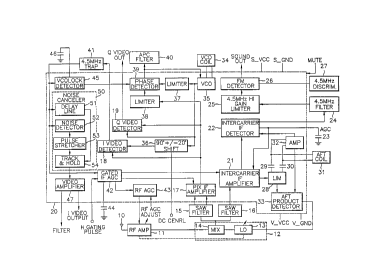
FIGURE 1 is a schematic bloc~C diagram of a high-
performance, intermediate-frequency integrated--circuit and
z5 peripheral circuitry for inclusion in television signal
receiver, as embody the invention and can be incorporated
into a television set or into television signal recording
apparatus.
FIGURE 2 is a plot of the response of the SAW filter
30 preceding the first intermediate-frequency amplifier in the
FIGURE l apparatus.
FIGURE 3 is a plot of the response of the SAW filter
preceding the second intermediate-frequency amplifier in
the FIGURE Z apparatus.
35 FIGURE 4 is a detailed schematic diagram of the gain-
controlled first voltage-amplifier stage in the second
intermediate-frequency amplifier used for intercarrier
sound and AFT in the FIGURE 1 apparatus.
- 6 -
FIGURE 5 is a detailed schematic diagram of the gain-
controlled second voltage-ampiifier stage, the fixed-gain
third voltage-amplifier stage, and direct-coupled
differential-mode feedback circuitry in the second
intermediate-frequency amplifier used for intercarrier
sound and AFT in the FIGURE 1 apparatus.
FIGURE 6 is a more detailed schematic diagram of the
portion of the FIGURE 1 apparatus used for limiting the
picture carrier as translated to an IF and developing from
this limited carrier an automatic fine tuning (AFT) signal
for controlling the frequency of the local oscillator used
to supply signals for heterodyning with the received
television signal when downconverting it to intermediate
frequencies.
FIGURE 7 is a detailed schematic diagram of the video
detector used in the FIGURE 1 apparatus for generating 4.5
MHz intercarrier sound intermediate frequencies and
connected after the FIGURE 4 second intermediate-frequency
amplifier.
FIGURE 8 is a detailed schematic diagram of an
overload automatic gain control (AGC) detector for the
FIGURE 4 second intermediate-frequency amplifier in the
FIGURE 1 apparatus.
DE'fAIhED DESCRZPTTOI~1 ..
In FIGURE 1 television signals, as may be received
off-the-air by a television antenna 10 as shown, from a
cable television system, or from a video tape recorder are
supplied to a radio-frequency amplifier 11. The RF
amplifier 11 supplies its amplified response to a selected
television'signal to a downconverter 12, which includes a
local oscillator 13 tuned together with the RF amplifier 11 '
to select one television signal for mixing and a mixer 14
for mixing the selected RF signal with the oscillator 13
oscillations. The mixer 14 generates the intermediate
frequencies and their image frequencies supplied to
surface-acoustic-wave (SAW) filters 15 and 16.
The SAW filter 15 selects the intermediate frequencies
~~.?~~a~~
_~_
from their image frequencies for application in balanced
form to a first intermediate-frequency amplifier 17, the
amplified first-IF-amplifier response from which is
supplied to an in-phase synchronous video detector 18 and
to a quadrature-phase synchronous video detector 19. Since
the first IF amplifier 17 supplies amplified picture
carrier and its amplitude-modulation sideband to the video
detector 18 for detection to recover composite video
signal, the amplifier 17 is also referred to as the
"picture°' IF amplifier or "PIX" IF amplifier. The
synchronous video detectors 18, 19 and the first IF
amplifier 17 are shown as being disposed within the
confines of a monolithic integrated circuit 20 indicated by
dashed line in FIGURE 1. The SAW filter 15 has a
conventional frequency response for television IF
circuitry.
FIGURE 2 shows the SAW filter 15 response, presuming
a 45.75 MHz video IF carrier frequency to be used, which
response includes a relatively deep (>40 dB) trap at the
adjacent-channel sound-carrier frequency of 47.25 MHz.
This deep trap causes the response to the 45.75 MHz video
IF carrier frequency to be located on a downward slope in
frequency response, about 6 dB down. The response to the
in-channel sound-carrier frequency of 41.25 MHz is reduced
by about 30 dB. The SAW filter 15 exhibits linear-phase
response throughout its passband. An example of a SAW
filter exhibiting this type of response is the SAF45 MVB8oZ
manufactured by Murata Manufacturing Co., Ltd., in Erie,
Pennsylvania:
The SAW filter 16 selects the intermediate frequencies
generated by the mixer 14 from their image frequencies, for
application in single-ended form to a second intermediate-
frequency amplifier 21. The response characteristics of
the filter 16 are chosen to facilitate the production of
sound intermediate-frequency signals by the intercarrier
method, so the second TF amplifier is labelled as the
°'intercarrier" IF amplifier in FIGURE 1 of the drawing.
The amplified second-IF-amplifier response from the second
.,,,.,
re.'
_$_
IF amplifier is supplied to an exalted-carrier detector 22
included together With the amplifier 21 within the IC 20.
The exalted-carrier detector 22 develops, heterodyning the
amplitude-modulated video carrier and the frequency-
modulated audio carrier as translated to TF, thereby to
generate the sound IF signals as a frequency-modulated
difference carrier (at 4.5 MHz for HTSC television
signals). The response of the exalted-carrier detector 22
as supplied from a high-resistance source is lowpass
filtered by a shunt capacitor 23 located off the IC 20, to ..
develop an automatic gain control (AGCj signal for
controlling the gain of the second intermediate-frequency
amplifier 21. The response of the exalted-carrier detector
22, as supplied from another high-resistance source, is
bandpass filtered by a 4.5 MHz center-frequency filter 24
located off the IC 20, to separate intercarriersound-
intermediate-frequency signal for application to a limiter
25. The limiter 25 supplies limited intercarrier-sound 2F
signal to an FM detector, supplying an IC 20 sound output
signal and being shown as a type that uses a 4.5 MHz
discriminator circuit 27 located off the IC 20. The 4.5 MHz
discriminator circuit 27 may comprise an LC circuit oT a
ceramic filter, to mention specific examples. The
remaining portion 26 of the FM detector and the preceding
limiter 25 are disposed within the IC 20. The IC 20 sound
output signal may subsequently be amplified for application
to a loudspeaker; or, alternatively, the sound output
signal may subsequently be supplied to a stereophonic sound
detector, and the detected left-channel and right-channel
stereo sound signals derived from the IC 20 sound output
signal are then amplified for application to respective
loudspeaker's .
The second-IF-amplifier response supplied from the
intercarrier IF amplifier 21 is also supplied to a limiter
28 within the IC 20, which supplies limited second IF
amplifier response in push-pull via capacitors 29 and 30
within the IC 20 to a coil 31 located off the TC 20. The
coil 31 tunas against the capacitors 29 and 30 to provide
nominally-quadrature-phase response to the carrier portion
of the limited second-IF-amplifier response in balanced
form, as input to a carrier-wave amplifier 32 within the IC
20. The capacitors 29 and 30 block DC from the limiter to
the amplifier 32, which supplies amplified carrier wave to
the exalted°carrier detector 22 and to a phase detector 33
within the TC 20. The coil 31 has a high Q, so its tuning
against the capacitors 29 and 30 provides a nominally
quadrature phase shift that is in fact markedly frequency-
dependent. The phase detector 33 measures the phasing of
the carrier supplied by the amplifier 32, respective to the
limited second-IF-amplifier response, for generating an
automatic fine tuning (AFT) signal to control the frequency
and phase of the local oscillator 13 in the downconverter
12.
FIGURE 3 shows the SAW filter 16 response, presuming
a 45.75 MHz video IF carrier frequency to be used, which
response is double-humped in nature. A first of the humps
has a peak at 41.25 MHz, the IF frequency to which the
sound carrier is translated during the first detection
procedure, which is a superheterodyning taking place in the
mixer 14; and a second of the humps has a peak near 45.75
MHz, the IF frequency to which the picture carrier is
translated during the first detection procedure. The SAW
filter 16 response also includes a relatively deep (>40 dB)
trap at the adjacent-channel sound-carrier frequency of
47.25 MHz. Even if the 45.75 MHz picture carrier is
slightly higher in frequency than the peak of the second
hump, so it is down by 2 dB or so, it will be bigger than
the 41.25 MHz sound carrier. The picture carrier not being
further down on the slope into the trap helps the AFT in
distinguishing the picture carrier from in-channel and
adjacent-channel sound carriers. The saddle between the
humps at 41.25 MHz and near 45.75 MHz is only 6 dB down or
so, maintaining AFT pull-in capability through this
frequency range while offering reduction of sound beats
generated when video baseband components near 2.25 MHz
double to 4.5 MHz.
Alternatively, the saddle can be eliminated completely so
midband response is flat, as shown by the dotted line in
- 10 -
FIGURE 3; or the saddle can be reduced to be between the
characteristics shown in FIGURE 3.
The 41.25 MHz sound carrier in the signal the SAW
filter 16 response supplies to the sound IF amplifier 21
should be at least 10 dB down from the 45.75 MHz picture
carrier, so the AFT detector cannot be captured by the in-
channel so~znd carrier. Since the sound carrier is about 18
dB down respective to the picture carrier in the
television signal received at the RF amplifier 11 and
downconverted in the mixer 12, the humps at 41.25 MHz and
near 45.75 MHz in the SAW filter response to a flat
bandsweep can be at substantially the same insertion loss
level without risk of the AFT detector being captured by
the in-channel sound carrier, even when adverse reception
conditions tend to null the picture carrier respective to
the sound carrier.
Referring back to FIGURE 1, a voltage-controlled
oscillator (VCO) includes a tank coil 34 located off the IC
and a remaining portion 35 located within the IC 20,
20 which includes a tank capacitance and a regenerative
amplifier. Oscillations nominally at 45.75 MHz picture
carrier frequency, as supplied by this vCO, are applied
directly as quadrature carrier to the quadrature-phase
video detector 19 and via a dc-controlled nominally-900
phase shifter 36 as in-phase carrier to the in-phase video
detector 18. The oscillations from this VCO 34, 35 and the
response of the first (PIX) IF amplifier 17 are
respectively supplied to limiters 37 and 38; and the ..
square-wave responses of the limiters 37 and 38 are
supplied to a phase detector 39, which generates an
automatic frequency and phase control (AFPC) voltage for
the voltage-controlled oscillator 34, 35. An AFPC filter 40
located off the IC 20 provides smoothing to this AFDC
voltage:
The video signal detected by the in-phase video
detector 18 is passed through a 4.5 MHz sound IF trap
filter 41 located off the IC 20. The video signal response
', . ~.:' w: ': ~ . y ,.:;.. ',:, ,.. . :;;:.. , .
n, . ~,.: ,..s~ .
,. ;-y ,-Fa... , ,,
... .t. _; ".~-,;;.~,~,;- , . _ , ' _
~ ~ , ': ~ . .. , .,... .. , .
_ . : . , ..
'
~
w . ; ~ .. :: , -~: .. ~ . ,' , . ..
. s .
, .
~~~~~a~
- 11 -
of the sound IF trap filter 41 is supplied to IF AGC
circuitry 42 for developing automatic-gain-control (AGC)
signals for application to the first (P2X) YF amplifier 17,
to the second IF (intercarrier) amplifier 21 and to a
delayed-AGG circuit 43 for developing delayed automatic-
gain-control (AGC) signals for application to the RF
amplifier 11. An off-chip capacitor 44 connects from a
point in the IF-AGC circuitry 42 to ground reference
potential as part of the lowpass faltering of the IF-AGC
signal developed by the IF-AGC circuitry 42.
The video signal response of the sound IF trap filter
41 is also supplied to a VCO lock detector 45 that detects
whether or not the oscillations from the VCO 34, 35 are
locked in frequency and phase with the picture carrier in
the signal from the PIX IF amplifier 17. When the
oscillations from the VCO 34, 35 are in lock with the
picture carrier in the signal from the PIX IF amplifier 17,
the detection of the video modulation is in a prescribed
direction from a baseline value of voltage. In a
particular embodiment of the FIGURE 1 apparatus
specifically referred to far purposes of description, a
video signal that exhibits negative excursions from a +2
volt baseline value, extending down to +1 volt on sync
tips, is synchronously detected by the in-phase synchronous
video detector 18 when the VCO 34, 35 is in lock, providing
the signal from the video IF amplifier 17 is not
accompanied by impulse noise. When the VCO 34, 35 is out
o~ lack, the operation of the in phase video detector 18 is
non-synchronous; and the detector response alternately
swings positive and negative responsive to the phase
slippage between the VCO 34, 35 oscillations and the
picture carrier in the signal from the video IF amplifier
17. The VCO lock detector 45 detects swings of the in-
phase video detector 18 that are positive respective to the
+2 volt baseline value by more than a half volt or so, to
provide an indication of lack of lock between the VCO 34,
35 oscillations and a picture carrier in the signal from
the video YF amplifier 17. When the signal from the video
IF amplifier 17 is accompanied by impulse noise, the
~~;?~~5~~
12 -
operation of the in-phase videa detector 18 is non-
synchronous; and, if unfiltered, the detector response
would alternately swing positive and negative responsive to
the phase slippage between the VCO 34, 35 oscillations and
the ringing of the SAW filter Z5 response in the presence
of impulse noise, continuing until the ringing subsides.
An off-chip capacitor 46 connects from a point in the VCO
lock detector 45 to ground reference potential as part of
lowpass filtering of the lack of lock indications that
suppresses lack of lock indications generated in response
to impulse noise. The VCO lock detector 45 responds to
sustained lank of lock to supply indication thereof to the
phase detector 39, which generates AFDC voltage for the VCO
34, 35. Responsive to the indication of sustained lack of
lock, the gain of the phase detector 39, which is very high
during in-lock condition, is reduced during out-of-lock
condition. This reduction of the phase detector 39 gain is
accompanied by an extension of the frequency range over
which the VCO 34, 35 will pull into lock.
The video signal, as detected by the in-phase video
detector 18 and passed through a 4.5 MHz sound IF trap
filter 41, can be supplied directly to a video amplifier 47
that supplies amplified in-phase video response to be used
off-chip. The amplified in-phase video response is
supplied, for example, to a horizontal sync separator and
pulse shaper for generating the horizontal gating pulses
supplied back to the IC 20.
FIGURE 1 shows the video signal, as detected by the
in-phase video detector 18 and passed through a 4.5 MHz
30'sound IF trap filter 41, being supplied to the video
amplifier 47 via impulse-noise-cancelation circuitry 50.
The impulse-noise--cancelation circuitry 50 is of a type
described in detail and claimed in U. S. patent application
serial No. 07/897,812 filed 12 June 1992 by Jack Rudolph
Harford, entitled NOISE REDUCING APPARATUS AND METHODS FOR
TELEVISION RECEIVERS, and assigned to Samsung Electronics
Co., Ltd. The impulse-noise-cancelation circuitry 50
comprises a delay line 51, a noise detector 52, a pulse
_.
~~~~~5~1
- 13 -
stretcher 53 and a track-and-hold Circuit 54. The noise
detector 52 detects, in the video signal from the sound IF
trap filter 41, black-going impulse noise that swings past
reference black level or white-going impulse noise that
swings the opposite way respective to a baseline reference
voltage that normal video does. The oR'ed response to
these impulse conditions is stretched slightly by the pulse
stretcher 53, to furnish a signal to the track-and--hold
circuit 54 that conditions it to hold the last value of its
output signal. Otherwise, the output signal of the track-
and-hold circuit 54 tracks its input signal, a delayed
response to the video signal from the sound IF trap filter
41 supplied by the delay line 51. The delay line 51
compensates for delay incurred by the noise detector 52
and the pulse stretcher 53 in performing their functions.
The video signal from the track-and-hold circuit 54, which
has .impulse noise replaced by a continuing value of video
signal, is applied to the video amplifier 47 as its input
signal in FIGURE 1.
FIGURE 4 is a detailed schematic diagram of the gain-
controlled first voltage-amplifier stage in the second -
intermediate-frequency amplifier 21 in the FIGURE 1
apparatus. Terminals T1 and T2 provide for connections to
the positive and negative terminals of an operating voltage
supply. The substrate of the monolithic TC is " grounded"
'to the terminal T2, and dux°ing operation all potentials on
the IC are positive respective to the B+ potential at the
terminal T1.
A direct voltage 3.5 times as large as the emitter-
base offset potential VDT is developed across the series
connection of the emitter-to-collector paths of NPN
transistors Q 1, Q 2 and Q 3 responsive to current flowing
through them via a resistor R] from the B+ positive
operating supply. Q1 and Q2 are self-biased by direct
collector-to-base connections to develop respective VBE
offsets across their emitter-to-collector paths responsive
to the current flow therethrough, and resistors R2 and R3
form a resistive potential divider providing direct-coupled
.... .' a'n' ...;: ~.... ..;',
Z ',:y: '..:.' ... ...... ~. .~: .:: _~:.~ %' ,.:. ~::' . '. ~::~. ,...
.., -.' '.
. . . :. ". :.. ::: ... . ,
: ~
~
v.:i ., , :,,', . , .: . ,:. .. .. . .'':
~1~, ' ~y ,. ' ~ . ..
..~.
~~
, ', _ . '~ .,; ,
.. , , . :, ; ,
., :. . . -,.. ', , _ $ . ~ :.. '.. ' ,
,
; .' . . . ' : .. ,. . ~; ..~
'.
.,
- 14 -
degenerative collector-to base feedback to Q3 for
developing a 1.5 VDE offset across its emitter-to-collector
path responsive to the current flow therethrough.
A resistor R~ applies the resulting 3.8 VBE offset from
integrated-circuit ground, appearing at a node N1, to an
input terminal T3 that receives the response of the SAW
filter 16 and connects to the base of an NPN transistor Q4.
A resistor R5 applies that 3.5 VpE offset to the base of
another NPN transistor Q5. Resistors R6 and R7 provide
respective emitter loads for Q4 and Q5, which are connected
as common-collector amplifiers (or emitter followers) for
driving the bases of NPN transistors Q6 and Q7,
respectively. Q 6 and Q7 are connected in emitter-coupled
differential-amplifier configuration with respective
emitter degeneration resistors R8 and R9 connected to a
node N2, from which the collector currents of NPN
transistors Q8 and Q3 are withdrawn. Q8 and Q9 are
provided with respective emitter resistors R10 and R11, and
their bases connect to a node N3 for receiving a direct
bias potential, conditioning Q8 and Q9 to function as
constant current generators for withdrawing current from
the node N2.
Q6 and Q7 supply collector currents that exhibit
balanced amplified response to the single-ended SAW filter
16 response applied to the input terminal T3. These
collector currents are supplied to respective current
splatters, used in the automatic gain control (AGC) of the
emitter-coupled differential-amplifier configuration in
which Q6 and Q7 are connected. NPN transistors Q10 and Q11
are connected as a current-splatter for the collector
current of Q6, with the emitter of Q10 directly connected
to the collector of Q6 and with the emitter of Q11
connected to the collector of Q6 via a resistor R12. The
NPN transistors Q12 and Q13 are connected as a current-
splatter for the collector current of transistor Q7, with
the emitter of Q12 directly connected to the collector of
Q7 and with the emitter of Q12 connected to the collector
of Q7 via a resistor R 2 3. The bases of Q10 and Q12
~~~~~~'I
- 15 -
connect to the emitter of an NPN transistor Q14 for
receiving a positive direct bias potential; and the bases
of Q11 and Q13 connect to the emitter of an NPN transistor
Q15 for receiving a gain control voltage. The collectors of
Q10 and Q12 connect to nodes N4 and N5, respectively, which
are connected via resistors R14 and R15, respectively, to
a node N6. A series dropping resistor R16 connects from
the B+ terminal T1 to the node N6, which is a "virtual
ground" for AC signal.
Further to implement the AGC of the emitter-coupled
differential-amplifier configuration in which Q6 and Q7 are
connected, an electrically controllable conductance is
Provided between nodes N4 and N5. The joined collector and
base of an NPN transistor Q16 as well as the collector of
Q10 connect to the node N4. The joined collector and base
of an NPN transistor Q17 as well as the collector of Q12
connect to the node N5. The emitters of Q16 and Q1? and
the collectors of Q11 and Q13 are all conductively joined
at a node N7 to which the node N6 is connected via a
resister R17.
In operation, the collector output current of
differential-amplifier transistor Q6 constitutes the tail
current of differential pair transistors Q10 and Q11, which
function as a current-split~ter. Depending on the control
signal level at the emitter of Q15, the collector output
current of differential-amplifier transistor Q6 can be
steered through transistor Q10 or through transistor Qil
and thence through diode-connected transistor Q16, or
partly through each of the transistors Q10 and Q11. In
symmetrical fashion, the collector output current of .
differential-amplifier transistor Q7 can be steered through
transistor Q12 or through transistor Q13 and thence through
diode-connected transistor Q17, of partly through each of
the transistors Q12 and Q13.
The steering of currents to flow entirely through Q11
and Q13 applies the entire collector currents of Q6 and Q7
including their differential variations i:o the node N7,
~ C1 ~ ;-~ ~... I
~~~~~Uz.~tx
- 16
where the differential signal variations cancel each other
out at another "'virtual ground" for AC. There are no
components of Q10 and Q12 collector currents flowing
through Q11 and Q13, the differential variations of which
can respectively flow to the load resistors R14 and R15 to
cause corresponding balanced-signal voltages across them.
The common-mode pC components of the collector currents of
Q6 and Q7 are in combined flow through the diode-connected
transistors Q16 and Q17, causing their conductances to
ZO become relatively small respective to those of the load
resistors R14 and R15, respectively. The low shunt
resistances of the diode-connected transistors Q16 and Q17
determine the valtage gain of the emitter--coupled
differential-amplifier connection of Q6 and Q7 as they
ratio against resistances of resistors R14 and R15,
respectively. When the combined collector currents of Q6
and Q7 are steered through diode-connected transistors Q16
and Q17, the gain will be at its minimum level.
The steering of currents to flow entirely through Q10
and Q12 applies the entire collector currents of Q6 and Q7
including their differential variations to the load
resistors R14 and R15, respectively. The concomitant
steering of currents away from Q11 and Q13 results in no
current being steered through the diode-connected
transistors Q16 and Q17, so their conductances are
accordingly very low and do not shunt the load resistors
R14 and R15 appreciably. The voltage gain of the emitter-
coupled differential-amplifier connection of Q6 and Q7 is
therefore is at its maximum level.
~ The steering of the collector currents of Q6 and Q7
only partially through Q10 and Q12 reduces gain by applying
only a fraction of the differential variations of the Q6
and Q7 collector currents to the load resistors R14 and
R15, thereby reducing the corresponding signal voltages
across them in a degree controlled by the departure of the
gain control potential at the emitter of Q15 from the
direct bias potential at the emitter of Q14. The steering
of the collector currents of Q6 and Q7 partially through
. .
-'~vJ
- 17 -
Q11 and Q13 at the same time further reduces gain by
causing the common-mode components of the collector
currents to flow through the diode-connected transistors
Q15 and Q17, so their conductances shunt the load resistors
R14 and R15 in a degree also controlled by the departure of
the gain control potential at the emitter of Q15 from the
direct bias potential at the emitter of Q14.
In any case, the total current in resistor R14 remains
unchanged during the gain control process, being always
equal to the collector output current of transistor QE and
likewise, the total current in resistor R15 remains
unchanged during the gain control process, being always
equal to the collector output current of transistor Q7.
Thus, if the transistors are well matched, as the gain is
changed there will be no disturbance of the DC conditions
at the nodes N4 and N5.
FIGURE 4 also shows the circuitry used to regulate the
bias voltage on the node N3 to be around a volt or so. An
NPN transistor Q18 has its base connected from the node N3
and has its emitter connected via a resistor R18 to a point
of ground potential. A common-collector-amplifier NPN
transistor Q19 has a base to which the transistor Q18
connects and has an emitter connected to the node N3. The
emitter-follower action of the transistor Q19 provides
direct-coupled collector-to-base feedback for the
transistor Q18, which feedback conditions the transistor
Q18 to demand collector current. This demand for collector
current is met by current flow from the positive operating
voltage supply connected to the terminal B+, the current
Blow being'through the series connection of resistors R20,
R21 and R22; a forward-poled, diode-connected NPN
transistor Q20; and a further resistor R23. Points within
this series connection are used for providing direct
voltage bias to various portions of the FIGURE 4 and FIGURE '
5 circuitry.
The direct potential at the interconnected ends of R21
and R22 is somecahat more positive than the direct potential
at a node N6 to which the other end of R22 connects.
Direct potential at the node N8, to which the collector and
base of Q20 each connect, biases the base of Q 14. The
common-collector-amplifier transistors Q14 and Q15 have
respective emitter--load resistors R24 and R25 connecting
their emitters to points of ground potential. Q15 has its
base connected to a node N9. The direct potential at the
emitter of Q20 is applied to the base of a grounded-
collector PNP transistor Q21 to develop a direct bias
potential at the emitter of Q21 that tracks the node N8
potential and is applied to the node N9.
Absent positive current flow into node N9 either via
a resistor R27 or via a resistor R28, the base potential of
Q15 is less positive than that of Q14. The emitter
potential of Q15 is then less positive than that of Q14,
cutting off conduction through Q11 and Q13. Q10 and Q12
are conductive, applying the entire collector currents of
the emitter-coupled differential-amplifier transistors Q6
and Q7 to their respective collector load resistors R14 and
R15 to provide maximum voltage gain. The potential drop
across the resistor R22 provides for delayed AGC of the
first controlled-voltage-gain stage of the second IF
amplifier, so that gain is first reduced in the second
controlled-voltage-gain stage of the second IF amplifier.
A terminal T4 receives automatic-gain-control (AGC)
signal voltage from the IF-AGC circuitry 42 (shown in
FIGURE 1), which is applied to the base of a common-
collector-amplifier PNP transistor Q22, the emitter of
which connects to the B+ terminal T1 via an emitter load
resistor R29 and also connects to the base of a common-
collector-amplifier NPN transistor Q23. The cascaded
commoncollector amplifiers including Q22 and Q23 form a
zero-offset voltage follower for applying the AGC signal
voltage received at the terminal T4 to the end of the
resistor R27 remote from its end connected to the node N9.
The resistors R26 and R27 form a resistive potential
divider for applying a fraction of the AGC signal voltage
received at the terminal T4 to the base of Q15. As the AGC
.,, ~~~~~5~~
_ ig
signal voltage received at the terminal T4 becomes more
positive, current-splatter transistors Q11 and Q13 are
biased into increased canduction, to steal emitter current
from the common-base amplifier transistors Q10 and Q12 and
to increase the conduction of the diode-connected
transistors Q16 and Q17, both of which actions reduce the
voltage gain of the differential amplifier comprising the
emitter-coupled transistors Q6 and Q7 withdrawing balanced
collector currents through their respective collector load
resistors R14 and R15.
A terminal T5 receives an overload AGC signal voltage ~
generated by the FIGURE 8 circuitry in a manner described
further on in this specification and applied to the base of
a commoncollector-amplifier NPN transistor Q24. The
emitter of Q24 connects to the end of the resistor R28
remote from its end connected to the node N9. The
resistors R26 and R28 form a resistive potential divider
for applying a fraction of the overload AGC signal voltage
received at the terminal T5, as offset by the VBE emitter-
to-base potential offset of the emitter-follower transistor
Q24, to the base of Q15. As the overload AGC signal
voltage received at the terminal T5 becames more positive,
current-splatter transistors Q11 and Q13 are biased into
increased conduction, to steal emitter current from the
common-base amplifier transistors Q10 and Q12 and to
increase the conduction of the diode-connected transistors
Ql6 and Q17, both of which actions reduce the voltage gain
of the differential amplifier comprising the emitter-
coupled transistors Q6 and Q7 withdrawing balanced
collector currents through their respective collector load
resistors R14'and R15.
The potential at the interconnection of the resistors
R20 anc~ R21 is used to determine the operating potential
for the third voltage-amplifier stage of FIGURE 5. The
potential at the interconnection of the resistors R20 and ~ '
R21 is applied to the base of a common-collector-amplifier
PNP transistor Q25, the emitter of which connects to the B+
terminal T1 via an emitter load resistor R30 and also
.,
-20-
connects to the base of a common-collector-amplifier NPN
transistor Q26. The cascaded common-collector amplifiers
including Q25 and Q26 form a zero-offset voltage follower
for supplying the operating potential far the third
voltage-amplifier stage of FIGURE 5.
FIGURE 5 shows the gain-controlled second voltage-
amplifier stage, the fixed-gain third voltage-amplifier
stage and direct-coupled differential-mode feedback
circuitry in the second intermediate-frequency amplifier 21
of the FIGURE 1 apparatus. The AGC'd balanced response of
the emitter-coupled differential amplifier comprising Q6
and Q7, available at nodes N4 and N5, is coupled by the
emitter-follower action of the common-collector amplifier
transistors Q31 and Q32 to the bases of NPN transistors Q33
and Q34.
Q33 and Q34 are the emitter-coupled pair in a further
emitter-coupled differential amplifier, which also has AGC
applied thereto and is included within the gain-controlled
second voltage-amplifier stage. The AGC of this further
emitter-coupled differential amplifier differs from that of
the preceding emitter-coupled differential amplifier, since
the signal levels being controlled do riot vary over so wide
a dynamic range. Since the further emitter-coupled
differential amplifier is not exposed to overload on strong
signals, emitter degeneration of Q33 and Q34 is not
necessary, and their emitters connect directly to a node
N11 used as the tail connection. This permits AGC to be
carried forward, at least in part, through control of the
transconductances of Q33 and Q34 in response to varying
their emitter currents. This can be done by controlling
their combined emitter currents, withdrawn from the node
N11 as a tail current.
An NPN transistor Q35 has its base connected to the
node N 3 for receiving direct bias potential and has its
emitter connected to terminal T2 via a resistor R31, which
connections condition Q35 to demand a constant collector
current from a node N12. NPN transistors Q36 and Q37 form
- 21 _
a current-splatter, the emitter of Q36 connecting directly
to the node N12 and the emitter of Q37 connecting to the
node N1~ via a resistance R32. Q36 and Q37 form a current-
splitter, the collector of Q36 connecting to the node N11
to withdraw tail current therefrom, and the collector of
Q37 connecting to a node N13 to withdraw current therefrom.
Respective collector load resistors R33 and R34
connect from a node N14 to nodes N15 and N16, respectively,
to which the collectors of the emitter-coupled
differential-amplifier pair Q33 and Q34 respectively
connect. The node N14 is connected by a decoupling
resistor R35 to the B~- terminal T1. The joined collector
and base of a diode-connected NPN transistor Q38 connect
directly to the node N15, and its emitter connects directly
to the node N13. ~!'he joined collector and base of a diode-
connected NPN transistor Q39 connect directly to the node
N16, and its emitter connects directly to the node N13.
The node N13, which is a "virtual ground°° for AC, is
connected by a pull-up resistor R36 to the node N14, which
is also a "virtual graund" for AC. The diode-connected
transistors Q38 and Q39 provide an electrically
controllable conductance between nodes N15 and N16, which
conductance is controlled as an enponential function of the
collector current of Q37.
The direct bias potential developed at the node N8 in
the FIGURE 4 biasing circuitry is translated to lower
potential by the combined emitter-to-base offset voltages
of NPN transistors Q40 and Q41 for application the base of
Q36. Q40 and Q41 are connected as cascaded common-
collector amplifiers, or emitter followers, with respective
emitter load resistors R37 and R38 connecting their
emitters to ground terminal T2. The divided AGC potential
develaped at the node N9 in the FIGURE 4 AGC circuitry is
translated ~to lower potential by the combined emitter-to-
base offset voltages of NPN transistors Q42 and Q43 for
application the base of Q37. Q42 and Q43 are connected as
cascaded common-collector amplifiers, or emitter followers,
with respective emitter load resistors R39 and R40
- 22 -
connecting their emitters to ground terminal T2.
In the operation of the second controlled-voltage-gain
IF amplifier, collector current from Q35 is steered by the
transistor pair Q36 and Q37, between providing tail current
for the differential-amplifier transistors Q33 and Q34 on
the one hand, and providing bias current fox diode-
connected transistors Q38 and Q39 on the other hand. When
the diode-connected transistors Q38 and Q39 carry no
current, the gain is at its maximum value, being determined
by maximum tail current and by the collector load resistors
R33 and R34. When the translated divided AGC potential at
the base of Q37 is positive enough to bias Q37 into
conduction, the diode-connected transistors Q38 and Q39 are
biased into conduction, to shunt the collector resistors
R33 and R34 of Q33 and g34 to reduce their gain. At the
same time, the conduction of transistor Q37 reduces the
current available for flow through Q36 and as tail current
for Q33 and Q34. This reduced tail current operates Q33
and Q34 at reduced transconductance and thus reduces their
gain further. In any event, the DC through each of
resistors R33 and R34 is not disturbed by the operation of
gain control. However, when more than half of the
operating tail current for the differential amplifier pair
is steered into the diode-connected transistors Q38 and
Q39, noise performance will start to degrade. This is
because of the poorer noise figures of Q33 and Q34 as their
internal emitter resistances increase responsive to reduced
current conduction by the principal conduction path of
transistor Q36. Accordingly, the reduction of stage gain
by the shunting of the collector load resistors R33 and R34
by diode-connected transistors Q38 and Q39 is the mechanism
for gain reduction principally relied on, rather than
reduction of the transconductances of Q33 and Q34 through
starvation of their tail current. The normal range of gain
control is upward from about 0 dB, then, to 26 dB or so.
NPN transistors Q44 and Q45 are arranged as common-
collector-amplifiers, or emitter-followers, for applying
the balanced signals at the nodes N15 and N16 to a third
., ~1~G~5~
- 23 -
voltage-gain stage. The emitters of
Q44 and Q45
respectively connect to ends of resistors R41 and R42, the
other ends of which connected to ground terminal T2. The
gain-controlled, amplified, balanced TF signals at the
emitters of the emitter-follower transistors Q44 and Q45
are applied to the bases of NPN transistors Q46 and Q47,
which transistors Q46 and Q47 are a differential amplifier
pair having their respective emitters connected to a node
N17. Another NPN transistor Q48 has its base connected to
the node N3 for receiving direct bias potential and has its
emitter connected to integrated-circuit ground via a
resistor R43, which connections condition Q48 to demand a
constant collector current from the node N17. The
collectors of transistors Q46 and Q47 are connected via
respective resistors R44 and R45 to the node N10, to which
the bias circuitry shown in FIGURE 4 applies a positive , .
operating supply voltage that is reduced from that applied
to the Via- terminal T1.
The direct bias potentials on which the balanced IF
output signals at the collectors of transistors Q46 and Q47
are superposed are automatically adjusted by a
differential-mode direct-coupled DC feedback loop. The v
balanced IF output signals at the collectors of transistors
Q46 and Q47 are supplied to a four-terminal lowpass filter.
Resistors R46, R47, R48 and R49 and capacitances C1, C2, C3
and C4 are included in this four-terminal lowpass filter,
which supplies a balanced response to the bases of common
collector-amplifier NPN transistors Q48 and Q49. Q48 and
Q49 have respective emitter load resistors R50 and R51
connecting their emitters to a point at ground potential.
The balanced response applied to the bases of Q48 and
Q49 essentially consists of the direct bias potentials on
which the balanced IF output signals are superposed; and
Q48 and Q49 function as voltage followers of the emitter-
follower type for applying the difference between these
direct potentials between the bases of NPN transistors Q50
and Q51 connected in emitter-coupled differential amplifier
conguration. A node N18 at which their emitters
I~ ~ ~ ~ ~~
24 -
interconnect has the collector of an NPN transistor Q52
connected thereto. Q52 has its base connected to the node
N3 for receiving direct bias potential and has its emitter
connected to ground terminal T2 via a resistor R52, which
connections condition Q52 to demand a constant collector
current from the node N18. The collectors of the
transistors Q50 and Q51 are connected to withdraw balanced
currents from the emitters of the previously described
emitter-follower transistors Q32 and Q31, respectively, in
response to the difference between the direct potentials at
the collectors of transistors Q46 and Q47. These
connections close the direct-coupled, differential-mode DC
feedback loop used for eliminating any substantial
difference between these direct bias potentials.
NPN transistors Q53 and Q54 are arranged as voltage
followers of the emitter-follower type and serve as output
buffer stages. The bases of Q53 and Q54 have the
collectors of Q46 and Q47 respectively connecting to them,
and the collectors of Q53 and Q54 connect to the E+
terminal T1. The emitters of transistors Q53 and Q54
connect to ends of respective load resistors R53 and R54,
the other ends of which connect to ground. The emitters of
transistors Q53 and Q54 supply 400 mV, gain-controlled,
amplified, balanced IF signals at nodes N19 and N20, far
application to the intercarrier detector 22 used in the
FIGURE 1 apparatus for generating 4.5 MHz intercarrier
sound intermediate frequencies, and for application to the
limiter 28 used for limiting the picture carrier as
translated to an IF.
FIGURE'6 is a more detailed schematic diagram of the
portion of the FIGURE 1 apparatus used for limiting the
picture carrier as translated to IF and developing from
this limited carrier an automatic fine tuning (AFT) signal
for controlling the frequency of the local oscillator used
to supply signals for heterodyning with the received
television signal when downeonverting it to intermediate
frequencies. The AFT signal is developed by a quadrature
detector, as will be described after considering some
~~.~'~~5:~
- 25 -
details of the circuitry providing direct bias voltages and
currents to other portions of the Figure 6 circuitry.
Three constant current sinks are provided at the
respective collectors of NPN transistors Q55, Q56 and Q57,
which are the slave transistors of a plural-output current
mirror amplifier having an NPN transistor Q58 as Sts master
transistor. Q55, Q56, Q57 and Q58 have respective emitter
degeneration resistors R55, R56, R57 and R58 connecting
their emitters to the ground terminal T2. An NPN
transistor Q59 is connected as a common-collector amplifier
for providing direct-coupled collector-to-base feedback for
Q58. Q59 has an emitter load resistor R59 connected from
its emitter to the ground terminal T2, and its emitter
potential is applied directly to the bases of Q55, Q56, Q57
L5 and Q58. The input current into the current mirror
amplifier configuration comprising Q55, Q56, Q57, Q58 and
Q59 and their respective emitter resistors R55, R56, R57,
R58 and R59 is regulated by the current flow through the
series connection of resistors R60 and R61 from the B+
terminal T1. The direct bias potential appearing at the
interconnected ends of resistors R60 and R61 is applied to
the base of an NPN transistor Q60, which responds to that
direct bias potential for supplying by emitter-follower
action an intermediate operating supply voltage at its
emitter. A decoupling resistor R61 connects the collector
of Q60 to the B-~ terminal T1, and a capacitor C5 connects
from tile collector of Q60 to the ground terminal T2.
NPN transistors Q61 and Q62 are arranged as common-
collector-amplifiers, or emitter-followers, for the
balanced, amplified IF signals the FIGURE 5 circuitry
provides at the nodes N19 and N20. The emitters of Q6l and
Q62 respectively connect to ends of resistors R62 and R63,
the other ends of which connected to ground terminal T2. ..
The gain-controlled, amplified, balanced IF signals at
the emitters of the emitter-follower transistors Q61 and
Q62 are applied to the bases of NPN transistors Q63 and
Q64, the interconnected emitters of which connect to the
~~~~~~J~~
- 26 -
current sink provided at the collector of Q55. The
collectors of Q63 and Q64 are connected via respective
resistors R64 and R65 to the emitter of Q60, which supplies
them a positive operating potential. The signal supplied
between the base electrodes of Q63 and Q64 has about 400
mV, peak-to-peak swing, which tends to cause switched
alternative conduction of Q63 and Q64. During excursions
from the average value axis in a first polarity sense, Q63
is conductive and the constant collector current demand of
the current sink transistor Q55 is satisfied by current
flow through the resistor R64. During excursions from the
average value axis in a second polarity sense, opposite to
the first polarity sense, Q64 is conductive and the
constant collector current demand of the current sink
transistor Q55 is satisfied by current flow through the
resistor R65.
NPN transistors Q65 and Q66 are arranged as common-
collector-amplifiers, or emitter-followers, for the
balanced, symmetrically clipped "square," waves thus
developed at the collectors of Q63 and Q64. The emitters
of Q65 and Q66 respectively connect to ends of resistors
R66 and R67, the other ends of which connected to ground
terminal T2. The current sink transistor Q55, the emitter-
coupled differential-amplifier transistors Q63 arid Q64, the
collector load resistors R64 and R65 and the emitter-
follower connections of Q65 and Q66 provide the limiter 28
of FTGURE 1,
The capacitors 29 and 30 of FIGURE 1 correspond to
capacitors C6 and C7 in FIGURE 4, which capacitors 29 and
30 connect the emitters of Q65 and Q66 to terminals T6 and
T7 'respectively. The ends of the off-chip AFT coil 3Z
shown in FIGURE 1 connect to the terminals T6 and T7 of
FIGURE 4. The off-chip AFT coil 31 tunes against the
capacitors 29 and 30 to generate a nominally quadrature-
phase separated video carrier at the terminals T6 and T7 of
FIGURE 4. The terminals T6 and T7 connect to first ends of
resistors R68 and R69, the second ends of which connect to
a node N21. R68 and R69 reduce the Q of the tuned circuit,
~~~~~5~~.~
_ 27
so its phase response does not change too rapidly around
the picture carrier as translated to an IF. The tuned
circuit provides selectivity of frequency response for
separating from the balanced, symmetrically clipped
"square" waves at the emitters of Q65 and Q66 the picture
carrier as translated to an IF, reducing the need for
additional limner stages in order to provide additional
capture ratio further to suppress the sound carrier as
translated to an IF. The use of a single limiter stage to
develop the balanced, symmetrically clipped ''square" waves
to be filtered by this tuned circuit reduces the harmonic
content of the signal to be filtered, which reduces
tendencies towards developing spurious beats in the 4.5 MHz
sound-IF signal.
NPN transistors Q67 and Q68 are arranged as common-
collector-amplifiers, or emitter-followers, for the
quadrature-phase separated video carrier at the terminals
T6 and T7. The emitters of Q67 and Q68 respectively
connect to ends of resistors R70 and R71, the other ends of
which connected to ground terminal T2. The quadrature-
phase separated video carrier at the emitters of the
emitter-follower transistors Q67 and Q68 are applied to the
bases of emitter-coupled differential-amplifier NPN
transistors Q69 and Q70, the interconnected emitters of
which connect to an end of a tail resistor R72 connected at
its other end to the ground terminal T2. The collectors of
Q6~ and Q70 connect to a node N22 and to a node N23,
respectively, and thencefrom to the node N21 via respective
collector load resistors R73 ind R74. The node N21 is
connected via a decoupling resistor R75 to the R-+- terminal
T1: A capacitor C8 with plates respectively connecting to
the' node N2l and the ground terminal T2 bypasses the node
N21 for high frequencies. A capacitor C9 with respective
plates connecting to the nodes N22 and N23 cooperates with
the callector load resistors R73 and R74 for providing
additional phase shift to the amplified quadrature-phase
separated video carrier. The emitter follower connections
of Q67 and Q68 and the emitter-coupled differential-
amplifier connections of Q69 and Q70 provide the amplifier
!~~ ~~'fJr.~
- 28 -
32 of FIGURE 1.
The balanced, symmetrically clipped "square°' waves at .
the emitters of Q65 and Q66 are applied to the bases of NPN
transistors Q71 and Q72, which are emitter-coupled
differential-amplifier transistors the interconnected
emitters of which connect to the current sink provided at
the collector of Q56. The collectors of Q71 and Q72 are
connected via respective resistors R76 and R77 to the
emitter of Q60, which supplies them a positive operating
potential. The signal supplied between the base electrodes
of Q71 and Q72 has about 300 mV. peak-to-peak swing, which
tends to cause switched alternative conduction of Q71 and
Q72. During excursions from the average value axis in a
first polarity sense, Q71 is conductive and the constant '
collector current demand of the current sink transistor Q56
is satisfied by current flow through the resistor R76.
During excursions from the average value axis in a second
polarity sense, opposite to the first polarity sense, Q72
is conductive and the constant collector current demand of
the current sink transistor Q56 is satisfied by current
flow through the resistor R77. NPN transistors Q73 and Q74
are arranged as common-collector-amplifiers, or emitter-
followers, fox the balanced square waves thus developed at
the collectors of Q71 and Q72. The emitters of Q73 and Q74
respectively connect to ends of resistors R78 and R79, the
other ends of which connected to ground terminal T2. The
current sink transistor Q56, the emitter-coupled
differential-amplifier transistors Q71 and Q72, the
collector load resistors R76 and R77 and the emitter-
follower connections of Q73 and Q74 provide a further
limiter s~.age "stripping off" the amplitude modulation of
the picture carrier as translated to an IF, thereby
suppressing the sound carrier as translated to an IF so as
to increase capture ratio for the picture carrier as
translated to an IF.
The remaining portions of the FIGURE 6 circuitry may
be considered to be associated with the AFT product
detector 33 of FIGURE 1. The balanced, square waves at the
2g -
emitters of Q73 and Q74 are applied to the bases of NPN
transistors Q75 and Q76, which are emitter-coupled
differential-amplifier transistors the interconnected
emitters of which connect to the current sink provided at
the collector of Q57. The long-tailed pair connection of
NPN transistors Q75 and Q76 provides still further limiting
to the balanced, square wave currents corresponding to in-
phase separated video carrier demanded at the collectors of
Q75 and Q76. The collector of Q75 connects to the joined
emitters of NPN transistors Q77 and Q78. The collector of
Q76 connects to the joined emitters of NPN transistors Q79
and Q80. The bases of Q77 and Q79 connect to the nade N22,
and the bases of Q78 and Q80 connect to the node N23. The
collectors of Q77 and Q80 connect to a node N24, connected
via a resistor R80 to a node N25 and thencefrom to the B+
terminal T1 via one input circuit of a balanced-to-single-
ended converter; and the collectors of Q78 and Q79 connect
to a node N26, connected via a resistor R81 to a node N27
and thencefrom to the B+ terminal TI another input circuit
of that balanced-to-single-ended converter.
The capacitor C10 combines with the resistors R80 and
R81 to provide a lowpass filter for differential-mode
components of the collector currents of Q75 and Q76, as
split and recombined by connections of Q77, Q78, Q79 and
Q80. The capacitors C11 and C12 combine with the resistors
R80 and R81, respectively, to provide lowpass filters for
the common-mode components of the collector currents of Q75
and Q76, as split and recombined by connections of Q77,
Q78, Q7g and 5280~ This lowpass filtering suppresses the
intermediate frequencies and their harmonics.
The balanced-to-single-ended converter, with balanced
input connections at the nodes N25 and N27 and an output
connection to a terminal T8, comprises:
a first current mirror amplifier with input
connection at the node N25, with common
connection to the B+ terminal T1, and with output
connection at a node N28;
- 30 -
a second current mirror amplifier with input
connection at the node N27, with common
connection to the B,~ terminal T1, and with output
connection to the terminal T8; and
a thard current mirror amplifier with input
connection at the node N28, with common
connection to the ground terminal T2, and with
output connection to the terminal T8.
The first current mirror amplifier comprises a PNP
transistor Q81 with emitter degeneration resistor R82 as
master transistor, a PNP in-substrate transistor Q82 with
emitter load resistor R83 connected as an emitter-follower
to provide Q81 direct-coupled collector-to-base feedback,
and a PNP transistor Q83 with emitter degeneration resistor
R84 as slave transistor. The second current mirror
amplifier comprises a PNP transistor Q84 with emitter
degeneration resistor R85 as master transistor, a PNP in-
substrate transistor Q85 with emitter load resistor R86
connected as an emitter-follower to provide Q84 direct-
coupled collector-to-base feedback, and a PNP transistor
Q86 with emitter degeneration resistor R87 as slave
transistor. The third current mirror, amplifier comprises
an NPN transistor Q87 with emitter degeneration resistor
R88 as master transistor, an NPN transistor Q88 connected
as an emitter-follower to provide Q87 direct-coupled
collector-to-base feedback, and an NPN transistor Q89 with
emitter degeneration resistor R89 as slave transistor,
,, ,, ..
FTGURE 7 is a detailed schematic diagram of the
intercarrier detector 22 used in the FIGURE 1 apparatus.for
generating '4.5 MHz intercarrier sound intermediate
frequencies and connected after the second intermediate
fr~quency amplifier 2l. The sound-TF signal is developed
by a product datec~or used as mixer, as will be described
after considering some details of the circuitry providing
direct bias voltages and currents to other portions of the
Figure 7 circuitry.
- 31 -
Six constant current sinks are provided at the
respective collectors of NPN transistors Q90, Qgl, Q92,
Q93, Q94 and Q95, which are the slave transistors of a
plural-output current mirror amplifier having an NPN
transistor Q96 as its master transistor. Q90, Q91, Q92,
Q93, Q94, Q95 and Q96 have respective emitter degeneration
resistors R90, R91, R92, R93, R94, R95 and R96 connecting
their emitters to the ground terminal T2. An NPN
transistor Q97 is connected as a common-collector amplifier
for providing direct-coupled collector-to-base feedback for '
Q96. Q97 has an emitter load resistor R97 connected from
its emitter to the ground terminal T2, and its emitter
potential is applied directly to the bases of Q90, Q91,
Q92, Q93, Q94, Q95 and Q96. The input current into the
current mirror amplifier configuration comprising Q90, Q91,
Q92, Q93, Q94, Q95, Q96 and Q97 and their respective
emitter resistors R90, R91, R92, R93, R94, R95, R96 and R97
is regulated by the current flow through the series
connection of resistors R98 and R99 from the B+ terminal
Ti. The direct bias potential appearing at the
interconnected ends of resistors R98 and R99 is applied to w
the base of an NPN transistor QgB, which responds to that
direct bias potential for supplying by emitter-follower
action an intermediate operating supply voltage at its
emitter.
NPN transistors Q99 and Q100 are arranged as common-
collector-amplifiers, or emitter-followers, for the
balanced, amplified IF signals the FIGURE 5 IF amplifier
circuitry provides at the nodes N19 and N20. NPN
transistors Q101 and Q102 are arranged as common-collector-
aimplifiers, or emitter-followers, for the balanced,
amplified quadrature-phase Picture carrier as translated to
an IF the FIGURE 6 circuitry provides at the nodes N22 and
N23: The emitters of Q99, Q100, Q101 and Q102 connect to
the collectors of current sink transistors Q9o, Q91, Q92
and Q93, respectively.
The emitters of Q99 and Q100 are also connected to
apply balanced, amplified IF signals to the bases of NPN
,.
32 -
transistors Q103 and Q104, respectively. Q103 and Q104 are
emitter-coupled differential-amplifier transistors the
emitters of which connect via resistors 8100 and 8101,
respectively, to the collector of current sink transistor
Q~4. The emitter degeneration afforded by 8100 and 8101
linearize the emitter-coupled differential-amplifier
connection of Q103 and Q104. The collector of Q103
connects to the joined emitters of NPN transistors Q105 and
Q106. The collector of Q104 connects to the joined
emitters of NPN transistors Q107 and Q108. The bases of
Q105 and Q107 connect to the emitter of Q101, and the bases
of Q106 and Q108 connect to the emitter of Q102. Q101 and
Q102 are emitter-followers for the balanced, amplified
quadrature-phase picture carrier as translated to an IF
that the FIGURE 6 circuitry provides at the nodes N22 and
N23. The collectors of Q105 and Q108 connect to a node
N29, connected via a resistor 8102 to a node N30 and
thencefrom to the B + terminal T1 via one input circuit of
a balanced-to-single-ended converter; and the collectors of
Q]06 and Q107 connect to a node N31, connected via a
resistor 8103 to a node N32 and thencefrom to the E +
terminal T1 another input circuit of that balanced-to-
single-ended converter.
The capacitor C13 combines with the resistors 8102 and
8103 to provide a lowpass filter for differential-mode
components of the collector currents of Q103 and Q104, as
split and recombined by connections of Q105,Q106,Q1C7 and
Q108. The capacitors C14 and C15 combine with the
resistors 8102 and 8103, respectively, to provide lowpass
filters for the common-mode components of the collector
currents of Q103 and Q104, as split and recombined by
connections of Q105, Q106, Q107 and Q108. This lowpass
filtering suppresses the 40+ MHz intermediate frequencies
and their harmonics.
The balanced-to-single-ended converter, with balanced
input connections at the nodes N30 and N32 and an output
connection to a node N33, comprises:
- 33 -
a first current.'mirror amplifier with input
connection at the node N30, with common connection to
the B+ terminal T1, and with output connectian at the
node N33;
a second current mirror amplifier with input ,.
connection at the node N32, with common connection to
the B+ terminal T1, and with output connection to a
node N34p and
a third current mirror amplifier with input
connection at the node N34, with common connection to
the ground terminal T2, and with output connection to
the node N33.
The first current mirror amplifier comprises a pNp
transistor Q109 with emitter degeneration resistor 8104 as
master transistor, a PNP in-substrate transistor Q110 with
emitter load resistor 8105 connected as an emitter-follower
to provide Q109 direct coupled collector-to-base feedback,
and a PNP transistor Q111 with emitter degeneration
resistor 8106 as slave transistor. The second current
mirror amplifier comprises a PNP transistor Q132 with
emitter degeneration resistor 8107 as master transistor, a
PNp in-substrate transistor Q113 with emitter load resistor
8108 connected as an emitter-follower to provide Q113
direct-coupled collector-to-base feedback, and a PNP
transistor Q114 with emitter degeneration resistor 8109 as
slave transistor. The third current mirror amplifier
comprises an NPN transistor Q115 with emitter degeneration
xesistor 8110 as. master transistor, an NPN transistor Q116
with emitter load resistor 'R111 connected as an emitter-
follower to provide Q115 direct-coupled collector-to-base
feedback, and an NPN transistor Q117 with emitter
degeneration resistor 8112 as slave transistor.
A resistor 8113 connects from the emitter of Q98 to
the node N33 for biasing the node N33 to substantially half
B+ potential. The RG pi-section comprising a shunt
capacitor C16, series resistor 8114 and a shunt capacitor
;r
- 34 --
C16 provides a lowpass filter for separating the sound-IF
signal at the node N33 from its image. The sound-IF signal
as thus separated is applied to a voltage amplifier
comprising the cascade connection of a common-collector-
amplifier including an NPN transistor Q118, a common-base-
amplifier including an NPN transistor Q119, and a common- ".
collector-amplifier including an NPN transistor Q120; and
the resulting amplified sound-IF signal is supplied to a
terminal T9, for application to the 4.5 1~~ bandpass filter
2~1 as shown in FIGURE 1. More particularly, the emitter of ,
the common-collector-amplifier transistor Q118 drives the
emitter of the common-base-amplifier transistor Q119 via a
resistor 8115. The collector of the common-base-amplifier
transistor Q119 connects to the B+ terminal T1 through a
collector load resistor 8116, to provide voltage gain equal
to the quotient of the resistance of 8116 divided by the
resistance of 8115. The emitter potential of the common-
collector-amplifier transistor Q120 is divided by a
resistive potential divider comprising resistors 8117 and
8118, lowpass filtered by the RC section comprising a
series resistor 8119 and shunt capacitor C18, and applied
to the base of Q119, closing a negative feedback loop that
determines the quiescent biasing of the common-base-
amplifier transistor Q119. A small capacitor C19 shunts
the base of the emitter-follower transistor Q120 to ground
to further attenuate image components. A resistar 8120 is
connected to withdraw current to the ground terminal T2
from the emitter of Q119, so Q119 will not be cut-off by
positive excursions of the sound-IF signal at the emitter
of the emitter-follower transistor Q118.
FIGURE 8 is a detailed schematic diagram of the
overload AGC detector for the FIGURE 4 second intermediate-
frequency amplifier in the FIGURE 1 apparatus. The FIGURE
5 circuitry provides the FIGURE 8 overload AGC detector
balanced, amplified IF signals at the nodes N19 and N20.
An RC section comprising a series resistor 8121 and a shunt
capacitor C20 lowpass filters the signal at node N19,
extracting the direct bias potential thereof for
application to the base of an NPN transistar Q121. Q121 is
.-
- 35 -
connected as a common-collector amplifier and functions as
an emitter follower for supplying at its emitter a voltage
offset by 1 VHE from the direct bias potential at Sts base.
The emitter potential of Q121 is applied directly to the
bases of NPN transistors Q122 and Q123 connected as common-
collector amplifiers With emitter load resistors 8122 and
8123 respectively connecting their emitters to the ground
terminal T2. A resistor 8124 connects the emitter of Q121
to the emitter of Q122; and the 1 VBE offset potential
ZO between the base and emitter of Q122 causes current flow
through resistor 8124 supported by a substantially constant
emitter flow from Q121 that keeps the source impedance
offered at the emitter of Q121 reasonably low. The emitter
potential of Q121 is applied as quiescent bias potential to
the base of an NPN transistor Q124 via a resistor 8125. A
resistor 8126 connects the emitter of Q124 to the emitter
of Q122; and the 1 VeE quiescent potential appearing abross
resistor 8126 causes current flow therethrough which is
supported by a substantially constant emitter flow from
Q124. The emitter potentials of Q122 and Q123 are applied
to the bases of PNP transistors Q125 and Q126. Q125 and
Q126 are a long-tailed pair having their emitters connected
to a node N35 via a resistor 8127 and via a direct
connection without substantial impedance, respectively, and
having their collectors connected to nodes N36 and N37,
respectively. A tail resistor 8128 connects the node N35
to the N+ terminal T1.
The collector loading for Q125 and Q126 is a balanced-
to-single-ended converter, with balanced input connections
at the nodes N36 and N37 and an output connection to a node
N38, comprises:
a first current mirror amplifier with input
connection at the node N36, with common
connection to the ground terminal T2, and with
output connection at a node N39;
a second current mirror amplifier with input
connection at the node N37, with common
~1~?~~a~~
r-~
36 -
connection to the ground terminal T2, and
with output connection 'to the node N38; and
a third current mirror amplifier with .input
connection at the node N39, witty common .
connection to the B+ terminal T1, and with output
connection to the node N38.
The first current mirror amplifier comprises an NPN
transistor Q127 with emitter degeneration resistor 8129 and
direct-coupled collector-to-base feedback connection as
1Q master transistor, and a an NPN transistor Q128 with
emitter degeneration resistor 8130 as slave transistor.
The second current mirror amplifier comprises an NPN
transistor Q129 with emitter degeneration resistor 8131 and
direct-coupled collector-to-base feedback connection as
master transistor, and a an NPN transistor Q130 with
emitter degeneration resistor 8132 as slave transistor.
The third current mirror amplifier comprises a PNP
transistor Q131 with emitter degeneration resistor 8133 as
master transistor, a PNP in-substrate transistor Q132 with
emitter load resistor 8134 connected as an emitter-follower
to provide Q131 direct-coupled collector-to-base feedback,
and a PNP transistor Q133 with emitter degeneration
xesistor 8135 as slave transistor.
The voltage at the node N35 biases the base of a
,.
commoncollector-amplifier PNP transistor Q134, and the
vol age appearing at the emitter of Q134 owing to emitter-
follower action is applied via a resistor 8136 to the node
N38 tca determine its guiescent bias potential. The
potential at the node N38 is applied to the base of a
3O common-collector-amplifier NPN transistor Q135, and the
voltage appearing at the emitter of Q135 owing to emitter-
follower ac~iora is applied via a resistor 8137 to the
terminal T5. The terminal T5 is shunted to ground by the
off-chip capacitor 23 shown in FIGURR 1,
An NPN transistor Q136 with collector connected to the
B+ terminal T1 has the amplified IF signal superposed on a
::
~lw~~ ~~_~
- 37 -
quiescent voltage the FIGURE 5 circuitry provides at the
node N19 applied to its base. Q136 has its emitter
connected to a first plate of a capacitor C21, the second
plate of which connects to the emitter of an NPN transistor
Q137 arranged as a common-collector-amplifier for the
amplified IF signal superposed on a quiescent voltage the
FIGURE 5 circuitry provides at the node N20. Q137 has an
emitter load resistor 8138 connected from its emitter to
the ground terminal T2. During positive excursions of the
node Nl9 voltage from its average-value axis, the emitter-
follower action of Q136 charges the capacitor C21. The
resistor 8138 is of sufficiently high conductance that Q137
exhibits emitter-follower action during the concurrent
negative excursions of the node N20 voltage from its
average-value axis. Accordingly, the capacitor C21 is
charged to a voltage equal to the peak-to-peak excursion of
the balanced, amplified IF signals the FIGURE 5 circuitry
provides at the nodes N19 and N20. During the subsequent
positive excursions of the node N20 voltage from its
average-value axis, the voltage on the first plate of the
capacitor C21 is boosted above the average-value axis of
Q121 emitter voltage by a value one-and-a-half times the
peak amplitude of the positive excursions of the node N20
voltage from its average-value axis, as the emitter of Q137
swings up in potential. This boost in the base voltage of
Q124 is peak detected by charging a capacitor C22 connected
between the emitter of Q124 and the ground terminal T2.
As the peak-to-peak amplitude of the balanced,
amplified zF signals at the nodes N19 and N20 increases,
the voltage detected across the capacitor C22 increases,
reducing the conduction of Q126 respective to Q125. The
balanced-to-single-ended converter for the collector
currents of Q125 and Q126 responds to pull its output node
N38 to more positive potential. The emitter-follower Q135,
acting through the resistor R137,pulls up the potential at
terminal T5. As previously noted in descriptions of
FIGURES 4 and 5, sufficient rise in the potential at
terminal T5 reduces the gains of the controlled-voltage-
gain IF stages.