Note: Descriptions are shown in the official language in which they were submitted.
-' 21270~3
IMPROVED APPARATUS AND METHOD EMPLOYING POLARIZATION
MODULATION TO REDUCE EFFECTS OF POLARIZATION HOLE:
BURNING AND/OR POLARIZATION DEPENDENT LOSS
.
Technical Field
S This invention }elates ~o the optical transm~ n of illru.. nalion and,
more particularly, to improving trs~n~mi~cion capabilities over long-distance optical
tr~nsmi~ion paths employing le~eaLel...
Ba~ ;. ou..d of the I~ t~on
Very long optical fiber tran~misiion paths, such as those employed in
10 undersea or trans-cnntinçnt~l terrestrial lightwave tr~n~micsi~)n systems inrln(lin~
optical-~nnrlifier lcpeat~ ., are subject to decreased p~,lrul~ ce caused by a host of
possible i~ llr,~ , The i.~ llr.~; typically increase as a function of the length
of the optical l~i.n~"..ic~.on In long optical tr:lnimi~ion paths that include optical
~mrlifit~.rs, the illJ~ f~ tend to vary with time and cause a random fluctuation in
15 the signal-to-noise ra~io (SNR) of the optical tr~ngm~ n pa~ih. The random
fluct--~tir n in SNR contributes to a phenom~non known as signal fading. The SNRfl~ hl~tinn~ also result in an increased average bit error ratio (BER) in digital signals
being llo~ ;lt. d over the optical tranimi7~cio7~l path. When the SNR of a digital
signal being ~ JC~lt~,d on such an optical tr~n~mi~ion path becomes unacceptably20 small relative to the average SNR (resulting in an undesirably high BER), a signal-
to-noise fade is said to have occurred. F~ , ;..,elllal evidence has shown that the
signal fading and SNR n~lc~ ne are caused by a number of pol~ri7~tin~ epçn~ nt
effects induced by the optical fiber itself and/or other optical co-llponerl~. wit'nin the
tr~n~mi~ir.n path. In particular, one of these effects has now been i~1entifi~d as
25 pCl~Ti7~tion Illo.pçn~çnt hole burning (PDHB), which is related to the population
inversion dynamics of the optical ~mrlifiP.r~ A discussion of hole-burning can be
found in an article by D. W. Douglas, R. A. Haas, W.F. Krupke and M.J. Weber,
entitled "Spectral and pQl~ri7~tion Hole Burning in Neodymium Glass Lasers";
IEEE Journal of Quantum Electronics, Vol. QE-19, No. 11, November 1983.
PDHB reduces gain of the optical ~mplifiçrs within the long optical
tr~n~missio~ path for any signal having a state of polslri7~tion ("SOP") parallel to
that of a pol~ri7~,d primary optical signal carried by the tr~lncmis~ion path. However,
the gain provided by these ~mplifi~rs for optical signals which have an SOP
orthogonal to that of the primary signal remains relatively unaffected. The polarized
' 2127043
- 2 -
primary signal reduces the level of population inversion anisotropically within the
amplifier. This in turn, produces an isotropic saturation of the ~mplifi~r, which
results in a lower gain for optical signals in that SOP. This effectively causes the
arnplifier to ~lc;re~GII~ially enhance noise having an SOP orthogonal to that of the
5 primary signal. This çnh~ncecl noise lowers the SNR of the tr~ncmitt~-.d inform~tic-n
and causes an increased BER.
A prior method for reducing signal fading employs a two-wavelength
light source to transmit infr~rm~tion in two orthogonal states of pc l~ri7Rtinn over an
optical fiber tr~n~mi~ n path. Since this quasi-non-polarized light source shares its
10 optical power equally on any two orthogonal SOPs within the fiber, deleterious
polarization-~lepçn-lent effects may be reduced as long as the two wavelengths
remain orthog- n~lly pol,ori7~d along the optical tr~nemi~sir~n path. Other methods
employ polarization mr dul~t( rs between the optical signal source and the optical
tr~ncmics;on path to pçrio~icsllly mo~ te the pol~ri7S~tion state of the primarv15 optical inr .. ~ ou signal through a precleterminPd sequence of pol~ri7:~ti(~n states
such that, when averaged over the saturation time of the ~mplifi~J, all possibleprtl~ri7~tir,n states are excited with equal probability. These methods generally
employ single-stage polarization transformers that mrl1ul~tç the output SOP suchthat it traces p~riodir~lly an arbitrary but fixed great circle on the Poincare' sphere.
20 These mr,(lnlotr)rs, however, require that the optical signal l~llnf~h~d into the
pr~ lvri7oti~n m~l~llstrlr be in a stable and well-defined polarization state.
Summary of the I~ r.li(~..
The problems relating to pol~ri7~tir~n depçn~lent hole burning and/or
po1~ cn ~ nrle-~l loss are o~v..;ollle, in accol.lancv with the prinrirl~s of the
25 invention, by mr~ ting the state of pol~ri7Ation (SOP) of an optical signal being
l~lmrhPd into the tr~nsmi~ion path peri~ir~lly through a predetPrminP.d sequenceof polo ;~1;o/~ states. These time-varying pol~ri7~tion states are generated by a
co...h;n~;on of at least two pol~ri7~tion mo~lllo.~r)r~ which are operated at
s~,l,s~ iol1y differnt mr~ tion frequencies. For any given arbitrary input SOP to
30 the mr~llllotors, the COll-v~O~ g sequence of pv1~ri7SItion states is selected such
that averaged over the longest mr~ tion period, substantially all possible output
polarization states are excited with subst~nti~lly equal probability. This c~nt1ition is
fulfilled if, averaged over a full m~3ulsltir~n se~ll.ence, the three Stokes p~ of
the m~lll~ted pol~ri7~tir~n output states s 1, s2, and S3 are zero (0). Preferably, the
35 longest m~ul~tion period is sllbst~nti~lly shorter than the anisotropic saturation
time of the optical ~mplifier, which is typically of the order of 1 msec. The
CA 02127043 1998-02-02
polarization modulation is realized by employing two cascaded polarization modulators,
each of which produces a substantially different sequence of polarization states for the
same input polarization state than the other. The modulation sequences of the two
polarization modulators are selected such that the time-averaged Stokes parameters sl, s2,
5 and S3 of the modulated output polarization of the entire modulator cascade vanish for
any ~Ibillal y input polarization state to the modulators. Hence, the input SOP to the
modulator can be arbitrary and can even slowly vary with time.
In one exemplary embodiment of the invention, the modulator comprises two
cascaded rotating wave plates: a half-wave plate, spinning at a first constant angular
10 velocity, followed by a quarter-wave plate spinning at a second angular velocity different
from the first.
In another exemplary embodiment, the modulator comprises a cascade of two
adjustable phase retarders oriented at a fixed relative angle of 45~, and both of which
modulate the input optical signal to produce a periodic phase shift between -~ and +tc.
Additionally, for applications in which it is desirable to reduce effects of
polarization dependent loss, the SOP modulation frequencies are selected to be a multiple
of the information signal clock.
In accordance with one aspect of the present invention there is provided
apparatus intended for use in reducing the effects of polarization dependent hole-burning
20 in an optical tr~n~mi~sion system employing optical fiber amplifiers, the apparatus
comprising: means for generating an arbitrarily polarized optical signal; means for
modulating the state of polarization of said arbitrarily polarized optical signal
periodically through a predetermined sequence of polarization states such that averaged
over a predeterrnined modulation period substantially all possible output polarization
25 states are excited with substantially equal probability, said means for modulating
including first means for modulating the state of polarization of a particularly polarized
optical signal periodically between first and second states of polarization in at least one
pair of orthogonal polarization states such that substantially equal time is spent in each of
the first and second states of polarization and second means for modulating the state of
30 polarization of a particularly polarized optical signal periodically between first and
second states of polarization, where said state of polarization of the optical signal is a
symmetric combination of the input state of polarization of said first means formodulating and its orthogonal polarization state, and means for supplying said polarized
optical signal to said means for modulating.
CA 02127043 1998-02-02
- 3a-
In accordance with another aspect of the present invention there is provided a
method intended for use in reducing the effects of polarization dependent hole-burning in
an optical tran~mi~ion system employing optical fiber amplifiers, the method comprising
the steps of: generating an arbitrarily polarized optical signal; launching said polarized
optical signal; and modulating the state of polarization of said arbitrarily polarized
optical signal periodically through a predetermined sequence of polarization states such
that averaged over a predetermined modulation period substantially all possible output
polarization states are excited with substantially equal probability, said step of
modulating including a first step of modulating the state of polarization of a particularly
10 polarized optical signal periodically between first and second states of polarization, and a
second step of modulating the state of polarization of a particularly polarized optical
signal periodically between first and second states of polarization, where said state of
polarization of the optical signal is a symmetric combination of an input state of
polarization of said first step of modulating and its orthogonal polarization state.
15 Brief Description of the D. ~ J~S
FIG. 1 is a simplified block diagram of an arrangement including a polarization
modulator which facilitates the practice of the invention;
FIG. 2 shows a view of the waveguide and electrode structure of one
arrangement which may be employed for the polarization modulator of FIG. l; and
FIG. 3 shows a view of still another waveguide and electrode structure which
can be utilized for the polarization modulator of FIG. 1.
Detailed Description
FIG. 1 shows a simplified block diagram of an exemplary arrangement
facilitating the practice of the invention. As shown, the invention includes optical signal
25 source 100 which produces an optical information signal 102, polarization modulator 101
which modulates the SOP of optical information signal 102 to produce modulated optical
information signal 103, and optical tr~n~mi~ion system 104, into which the modulated
optical information signal 103 is launched. Optical information signal 102 is produced,
in well-known fashion, by a laser transmitter (not shown) in optical signal source 100.
21270~3
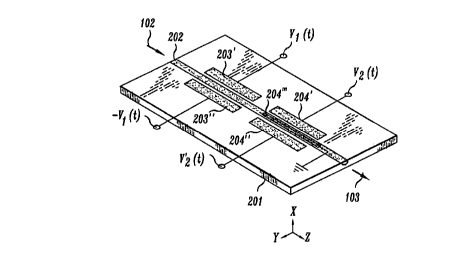
FIG. 2 shows one embodiment of polari_ation modul~tor 101 which
may be advantageously used in practicing the invention. An integrated optic
realization of pol~ri7~tion mod~ t~)r 101 is fabricated on low-birefrin~Pn~e X-cut,
Z-propagating LiNbO3 substrate 201 and operates with a standard titanium-
5 indiffused, single mode waveguide 202. It includes two electrode sectionscomprised of electrodes 203' and 203", and 204' and 204", leipec~ivt;1y, disposed
on substrate 201 on both sides of waveguide 202 and one common ground electrode
204"' on top of waveguide 202.
The first section of m~d~ tor 101, incl~ in~ electrodes 203' and 203",
10 operates to retard the linear pol~ri7S~tion colllponellt of the incoming optical signal
102 parallel to the X axis (TM mode) relative to the pol~ri7~tion co.l,~onellt of the
in- oming optical signal parallel to the Y axis (TE mode). The TE-TM mode phase
shiftisinducedviather22andrl2 (r22=-rl2= 3.4 10~l2m/V)electro-optic
coçfficiPnt~ by applying b~ nred drive voltage col~ onerll~ V 1 (t) and -V 1 (t) to
15 electrodes 203' and 203', respectively, thereby inducing an electric field Ey in
waveguide 202. The total induced phase shift ~(t) between the X and Y polarized
CO~ '' iS
~(t) = r (rl2-r22) ~,, ~ G ~ L n3 (1)
where t is time, ~ is the free-space wavelength, G is the gap between electrodes 203'
20 and 203', L is the length of electrodes 203' and 203~', nO is the ordinary index of
refraction and r is a nr-rm~li7P~ overlap pal~l~et~r between the optical and electrical
fields (0 S r ~
The second electrode section of m~dul~tt)r 101, inrlutling electrodes
204' and 204", operates to retard the linear polarization co" ~I .o~ I having an angle
25 of 45~ with respect to the X and Y axes relative to the linear pol~ri7~tir)n co---~,onelll
having an angle of -45~ with respect to the X and Y axes (TE-TM mode conversion).
TE-TM mode conversion is ~ccomrli~h~cl via the r6l (r6l = -r22)
electro-optic coefficient by applying comm-)n drive voltages V2 (t) and V2 (t)
= V 2 (t) to the side clccl-udcs 204' and 204", thereby infll-.~in~ an electric field E x
30 in the waveguide 202. The phase retardation rl (t) for mode conversion induced in
an electrode section of length L is
(t) - r r61 ;~, ~ , L nO (2)
G
2127043
where t is time, ~ is the free-space wavelength, G' is the gap between the ground
electrode 204"' and the side electrodes 204' and 204", L is the length of electrodes
204', 204" and 204"', nO is the ordinary index of refraction and r is the spatial
overlap of the applied electric field Ex with the optic fields (0 ~ r < 1).
S The pol~r17~tion transform~tion of mr~dnlsltor 101 shown in FIG. 2 can
be (lesrribed by a 3x3 Mueller matrix M, which relates ~he Stokes pa~ et~
s 1 ,s2 ,ands3 of the arbitrary polSIri7 ~tion state of optical h~ro. ,"silion signal 102 to
the Stokes p~dllletel~ of the modulated i~lrc,lmation signal 103. The ll~n~rc,lll.~lion
of the fLrst electrode section 203 is described by the ma~rix
0 0
M I = 0 cos2~(t) - sin2~(t) , (3)
~0-sin2~(t) cos2~(t),
and that of the second section by the matrix
cos2~(t) 0 sin2rl(t)
M2 = 0 1 0 (4)
~-sin2~(t) 0 cos2r~(t),
Hence, the overall ~ansf ~rm~ti- n of pols~ri7~tion m~ tl~r 101 is given by
cos2rl (t) - sin2~(t) sin2~ (t) cos2~(t) sin2rl (t)
M = M2- M1 = ~ cos2~(t) -sin2~(t) (5)
.-sin2rl(t) -sin2~(t)cos2rl(t) cos2~(t)cos2~(t),
For an arbitrarily polarized h~rc ., l . ~tir n signal 102, the time averaged
values of the Stokes pr~ n I~U t~ A S 1 ~ S 2 . and s 3 of the modulated optical inform~tion
signal 103 vanish if the time averaged values of all nine el~menti of the matrix M
are equal to ~ero. This is the case when the two electrode sections are driven by
voltages
Vl(t)= V~ T(Qlt), (6)
V2(t)= VO T(Q2t) +VT, (7)
V2(t)= Vo T(Q2t) -VT . (8)
,, , ~ - ~ ~ ;-; .: . . .- . .... .
212704~
- 6 -
where V0 is the voltage that induces complete TE-TM mode conversation (~ = 7~),
V ,~ is the voltage that induces a TE-TM phase shift of ~ ), and VT is the
voltage that reduces the residual, static birefringf nre in waveguide 202 substantially
to zero (0). The symmetric sawtooth function T is given, for example, by
T(Qt) = (-l)n 2 (Qt/~ - n) for 2n-1~2Qt/7~<2n+1, (9)
where Q 1 and n 2 are the two mn~ tion frequencies (Q I ~ Q 2 ), ~ iS the time, and n
is an arbitrary integer. Preferably, the two m~ tion frequencies are chosen suchthat Ql =2Q2 or Q2 =2Ql and Qi, i = 1, 2, subst~nti~lly larger than 2~/tS, wherets is the anisotropical saturation time of the optical amplifier (typically 1 ms). Then
10 all nine elemPnt~ of the matrix M vanish if averaged over a full period of the lower
of the two mo~ tion frequencies. To reduce the effects of polarization ~Ppen-lent
loss in the optical tr:~n~mie~ n system 104 (FIG. 1), the modnl~tion frequencies n
and Q2 are chosen to be integer multiples of the clock frequency of optical
inro~ ation signal 102.
If desired, s;~ oi~l drive voltages could be employed to provide the
m~ tion, namely,
Vl (t)=Q7655 V7~sin(Ql t), (10)
V2(t)=0.7655 VOSin(Q2t) +VT . (11)
V2(t)=0.7655 VOSin(Q2t) -- VT- (12)
FIG. 3 shows another embodiment of pol~ri7~tion mndnl~tcr 101 which
also may be employed in practicing the invention. Again, an integrated optic
reoli7flti~ n of pr~lori 7~tion mnd~ tor 101 is fabricated on low-birçf~ing~nre X-cut,
Z-propag~tin~ LiNbO3 substrate 201 and operates with a standard titanium-
in~lir~used, single mode waveguide 202. It includes two electrode sections,
compri~ed of electrodes 203' and 203", and 204' and 204", respectively, ~ pc~sed on
both sides of waveguide 202, and one comm()n ground electrode 205 on the top of
~.a~_guidG 202. In this e.nbo~ lGIlt of mod~ t~r 101, the first electrode section (
203' and 203" ) operates in a similar fashion to an endlessly rotating half-waveplate, i.e., it 5_.,e.~t~s a constant phase retardation of 7~ at a variable angular
30 ori~nt~tion This is achieved by in(llleing a variable combination of TE-TM phase
shifting and TE-TM mode conversion. The second electrode section (204' and 204")
2127043
- 7 -
operates in similar fashion to an endlessly rotating quarter-wave plate, gen~ g a
constant phase retardation ~/2 at a vanable angular onentsltic)n. TE-TM mode
conversion and TE-TM phase shifting are induced in a similar way as in the
embodiment of mc ~ tr~r 101 shown in FIG. 2 by applying drive voltages V 1 (t)
S and V2 (t) to side electrodes 203', 203", 204' and 204".
The dnve voltage V 1 (t) and V2 (t) applied to electrodes 203' and 203",
r~ eclively, are
V1(t) =VO Sin(Q1t) + V~COS(QIt) + VT ~ (13)
Vi (t) =Vo sin(nl t) -- V7~cos(Ql t) -- VT . (14)
10 where V0 is again the voltage that induces complPte TE-TM mode conversion
(Tl = ~), V7~ iS the voltage that induces a TE-TM phase shift of ~ ), and
VT is the voltage that reduces the residual, static birefring~.n~e in waveguide 202
s~lkst~nti~lly to zero (0).
When driven by these drive voltages V 1 (t) and Vi (t), the first section
15 (203' and 203") of pol on m~nl~tor 101 acts like a rotating half-wave plate spinning at a constant angular velocity of Q 1 ~
The drive voltages applied to electrodes 204' and 204", ~ ;kvely, are
V2(~) = (VO/2)sin(Q2t) + (v~/2)cos(Q2t)+vT~ ~15)
V2(t) = (VO/2)Sin(Q2t) -- (V,~/2)COS(Q2t) -- VT, (16)
20 where V0, V,~ and VT are as above in equations (13) and (14).
When driven with these voltages V 2 ( t) and V2 (t), the second section of
mo ll~ or 101 acts lilce a rotating quarter-wave plate spinning at a constant angular
velocity Q2
The p~ ion L~ ro~ ion produced by the spinning half-wave
25 plate is desrribed by the Mueller matrix
cos(2Qlt) sin(2Qlt) O
M3 = sin(2Qlt) -cos(2Qlt) 0 ~ (17)
O O -1
~r.~
2127043
- 8 -
.. ' :
and that produced by the spinning quarter-wave plate is given by
1 +cos(2Q2t) sin(2Q2t) 2sin(n2t)
M4 ~ 2 sin(2Q2t) l-cos(2Q2t) -2cos(Q2t) . (18)
-2sin(Q2t) 2cos(Q2t) 0
The overall L,an~rol.l.ation of polari_ation modulator 101 is then given
by
M = M4 ~ M3=
cos(2Q I t) +cos(2~52t) sin(2~Qt) - sin(2Q 1 t) - 2sin(Q2 t)
2 sin(2~S2t)+sin(2Qlt)-cos(2Qlt)+cos(2~Qt) 2cos(Q2t), (19)
2sin(2Q l t- Q2 t) - 2cos(2Q l t- Q2 t) 0 '
where~Q = (Q2 ~ Ql)-
Again, the time-averaged clF ,n~ of M vanish if Q 1 ~Q2, i.e., if the - --
half-wave and quarter-wave plates spin at different angular speeds. Preferably, the
10 two m~ stion L~ uen~,;es are chosen such that Q 1 = 1. S Q2, with Q 2 substsnti~lly
larger than 27~/tS, where the half-wave plate spins at 1.5 times the speed of the
quarter-wave plate. Another preferred operation of mod~ t-)r 101 is when
Q I = ~ Q 2, where the two wave plates spin in opposite di-~etions, but at the same
angular speed. It is also possible to set Q 1 = 2 Q2 if desired.
In all three cases the time-averaged Stokes p~, ~." ,. t . ;, s 1, s 2, and s 3 of
the output pol~ i, n of modlllst(~r 101 vanish for any arbitrary input pulsri7~ti~-n
state if averaged over a full period of the lower of the two m- dnl~tion r~ u~n- ;~s
Again, to reduce the effects of pol~ri7-s~tion-depen~lent loss, the m~ tion
Ç~ uenc;es Q 1 and S22 are selected to be integer multirl~s of the clock fieq,lcllcy of
20 optical in~o"~h~ion signal 102.
The above-desGribed arr~sng~mpnt~ are, of course, merely illu~ ivt; of
the appl~ stion of the principles of the invention. Other ~ ngem~nt~ may be
devised by those skilled in the art without departing from the spirit or scope of the
invention. Spe(~ifi~ y~ it is possible to replace either one of the two sections of
25 m~lll vstor 101 of FIG~ 2 by an element that produces vaTiable circular birefring~n~e,
such as a Faraday rotator, to produce a suitable modlll~tion se~lu~,nce in the
pc~lsri7stion state of signal 103. Likewise, it is feasible to replace the rotating half-
'
21~7043
,. g
~ wave and quarter-wave plate sections of mor~ tor lOl in FIG. 3 by generali~ed
i. wave plate sections, producing variable elliptical birefringence of constant phase
retardation ~ and 7~/2, respectively. It should further be understood that the
sequence of the two c~ec~ded sections of mod~ t(-r lOl may be reversed in the
5 embodiments of FIGs. 2 and 3 without affecting the operation of modnl~t( r lOl. It
is also possible to combine either one of the two sections of mocllllator lOl shown in
FIG. 2 with the half-wave plate section of modl1lAtor lOl shown in FIG. 3.
A-lrlititn~lly, mn(l~ tor lOl may comprise three (3) or more cS~cc~ded
mf d~ tor sections operated at s~1bst~ntiAl1y different mf)c~ tion frequencies such
10 that each of the sections produces a different modulation sequence of po1ari7~til~n
states than the previous section in the cascade. For exS~mr1~ the two sections of
po1~ri7~fion mf~--1 iSf r lOl of FIG. 2 may be followed or preceded by a rotating
half-wave plate section similar to that of FIG. 3, which is rotated at an angular speed
of, for example, Q3 = 3 Ql or Q3 = 3 Q2 -
It should further be understood by those skilled in the art that although a
titanium-il~fl;rr~leed waveguide structure for a lithium niobate mf dn1~tor is the
l,lefel.cd design, other waveguide form~til n.e are c~nt~mr1S~t~d and other substrates
may be employed inc111fl;ng but not limited to seminonductor m~t~.ri~1e Qnd lithium
t~nt~l~tf~ for ~ o Although not ~epecifir~1ly shown, it is to be undei~tuod that20 the mo(~ ted optical signal 103 is typically 1~llnnhf d from the m~ tr~)r lOl to the
optical ~ S~ oll system lO4 via an ~mp1ifif ati(~n stage or the like.
, .: : , ,- . ~ ~: ;.: - . ~, : , . .