Note: Descriptions are shown in the official language in which they were submitted.
2:~'.7~
P/60001/PS
Bare Die Testin~
Silicon integrated circuit devices (SICs) are processed in
wafer form and initial device testing is conducted on the completed
wafer prior to dicing, using a probe card or, more recently, a
membrane probe card, to make electrical contacts to the contact pads
of;the ICs under test. A~conventional probe card comprises a
radidl array of metallic probes supported in a circular aperture on
a printed circuit board~ The probes are provided with fine probe
tipS9 commonly fabricated using fine tungsten wire which has been
formed to a spherical tip shape at the point ot contact, with a
typica~l~tip diameter o~ 50 micrometres. The probe tips are
typically 0.5 mm in~length and 0.15mm diameterO Contact forces of
m~ 6 to 8 grams~per probe~are employed to ensure that low contact
resistance to the aluminium alloy metallisation pads on the IC is
- obtained. A probe set is expected to provide some 0O5 million
touch downs before replaceme~t. The probes are independantly
mounted and adjusted to ensure eonsistent contact. Tungsten is
selected as the probe material since it provides high hardness for a
low probe wear rate and low electrical resistivity for low probe
resistance.
: : :
;
~ ~7~
Device tests on wafer include basic parametric tests, low
frequency functional testing and, in some cases, speed bining tests
using specially designed test structures, or boundary scan testing.
The relatively high resistance and particularly the inductance of
the conventional probe card arrangement, however, precludes thorough
device testing at full operating frequency. A further constraint
on wafer level testing is associated with the finite test time
required to conduct a comprehensive functional test, particu1arly
when this testing is conducted at less than functional speed. The
mechanical difficulties associated with constructing conventional
probe cards for very high pin count ICs is one reason that
alternative probe card approaches are now being examined.
Once the ICs that have passed the wafer level probe testing
have been packaged, then comprehensive functional testing can
proceed. The package provides mechanical protection for the IC, to
allow straightforward device handling in the test system feeder, and
also a practical means of making contact to them device under test
through the package leads. Packaged devices may be fully
functionally tested at speed in generally acceptable test times.
A more recent advance in wafer level IC testing has been
the introduction of the membrane probe card structure. Here a
multilayer, flexible pcb interconnection structure is employed that
can provide controlled impedance, fine pitch traces to the location
of the pads of the device under test. Contacts to the device under
test àre made through plated gold bumps provided on the pcb trace
terminations, with the application of a suitable contact force and
wipe action. The multilayer pcb structure provides a ground plane
local to the signal traces to allow controlled impedance
interconnections to be realised from the test equipment electronics
through to the device under tes~. The membrane probe card does
allow higher frequency wafer level testing and is also far better
suited to the testing of high pin count devices. Temperature
testing with the membrane probe card approach is limited by the
membrane materials of construction to about 8~C.
2 ~
A microbumped test head which forms the subject of
co-pending Patent Application No. 920256000 is illustrated in the
cross-sectional diagram of Figure 1. Here the device to be tested
is held on the vacuum chuck of a flip chip apparatus with the active
device surface facing the test head substrate~ This flip chip
apparatus is very similar in construction to a flip chip bonding
equipment since it provides a means of picking up the bare die, of
aligning it with respect to the microbumps on the test head, of
bringing the device into contact with the test head and of applying
the required contact force. After the test good die are
transferred to an appropriate waffle pack container, while failed
die are rejected.
The apparatus may differ from a conventional flip chip
bonding apparatus only in its being used to provide a temporary
contact between the device and the test substrate rather than being
a means to a permanent connection. Flip chip bonding equipments
allow heating of die and/or substrate and this capability may also
be of use in the present application to allow bare die testing at
elevated temperature. The flip chip apparatus uses an op~ical
alignment method, for example an optical prism or semi-silvered
mirror arrangement that allows simultaneous viewing of the die and
substrate through solid state CCD camera or microscope optics, to
accurately align the bond pads of the device over the microbumps on
the substrate. In the case of the solid state CCD camera system,
an optical probe is inserted between the die and the substrate9
which are separated in space, for the alignment step. After
alignment, the optical probe is removed, the device is brought down
onto the microbump contact points and an appropriate contact
pressure and wipe action applied to ensure low contact resistance
(the s~epper motor control on such equipments allow wipe amplitudes
of a few micrometres to be employed for reliable contact but minimal
pad damage). Such equipments also allow accurate autocollimation of
the die and substrate surfaces to ensure parallelism and even
application of the applied force over the microbumps contacts.
.
r~ ~ r~ 1~
f~ r~
--4--
Flip chip bonding equipments are now becoming available that may be
used in the proposed bare die test mode with die handling rates of
many hundred die per hour.
The test head provides high interconnection density, high
bandwidth interconnections from the device under test, via the
microbump contact points, to the test equipment circuitry. The
substrate is constructed by thin film technologies, for example with
a multilayer aluminium-polyimide meta11isation structure, with
typical1y three or four layers of interconnect, a ground plane, a
power plane and one or two layers for signal trace routing. The
track geometries on the silicon substrate are between 10 and 25
micrometre line widths, with metal thicknesses of 2 to 5 micrometres
at track pitches of 40 to 100 micrometres, while dielectric
thicknesses are in the S to 20 micrometre range. Such geometries
allow controlled impedance, 50 ohm lines to be defined if required.
Alternative materials include copper as the conductor material and a
range of alternative polymers, including BCB and PPQ. This
interconnection technology geometry allows test access traces to be
easily routed into the d~vice under test area, while the low
parasitics of the interconnection traces and the well defined trace
impedances provide high bandwidthO The power and ground plane
structures provide high performance power and ground connections at
the site of the device under test.
According to one aspect of the present invention in a bare
die testing apparatus comprising a multilayer interconnection
structure providing a testing station for bare die, said testing
station having a plurality of microbumps of conductive material
located on interconnection trace terminations of said
interconnection structure and distributed in a pattern corresponding
to the pattern of contact pads on a bare die to be tested,
low-profi1e connections are provided to and from said
interconnection structure to permit testing of a die before
separation from a wafer.
The interconnection structure may be provided with one or
~ I h~ 7 ~
more apertures whereby a part or fully populated multichip module
may be tested. There may be provided means releasably to secure
said interconnection structure in position in said testing
apparatus.
A bare die testing apparatus in accordance with the present
invention will now be described by way of example with reference to
the accompanying drawings, of which:-
Figure 1 shows diagrammatically part of a known test headarrangement, and
Figures 2 to 6 show diagrammatically parts of dif~erent
multilayer interconnection structures for a testing apparatus in
accordance with the invention.
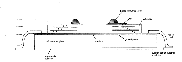
ReFerring to Figures 2, 4 and 5, the key feature is the
provision of connections from the test head to the surrounding test
circuitry that do not mechanically interfere with the lowering and
presenting of the microbump contacts to the wafer under test. Such
a constraint clearly does not arise in the testing of individual
devices. The ability to wafer level test is achieved by the use of
bond pad connections on the substrate periphery at the level of the
substrate itself and the use of low profile ribbon bonding to make
the connections between these bond pads and the supporting circuit
board. The typical total thickness of the multilayer metal and
dielectric of the substrate is 20 micrometres7 while the nickel
microbump may be some 30 micrometres in heightO A 10 to 15
micrometre thick, low profile ribbon bond may then be made that does
not rise above the allowab1e 50 micrometre limit. The substrate
base may be of silicon or sapphire or other transparent and
insulating~material. Sapphire, for example, can provide
transparency for alignment of the microbumps to the pads of the
devices on the wafer under test, and being insulating~ provides no
risk of edge shorting at the ribbon bond connections. An aperture
for alignment may be provided as required in the central region of
the multilayer metal and dielectric structure of the test head if a
transparent substrate is employed. The use of such an apparatus
, .
..
~ ~ 2 7 ~ r~ ~
-6-
then allows full functional, at temperature testing to be conducted
on wafers that may be diced for multichip module use or shipped in
whole wafer form for conventional packaging. The resulting
packaging of devices that have been fully functionally tested before
packaging means that packaging costs will only be incurred for good
die. The inability to fully test devices at the wafer level has, to
date, meant that a proportion of devices packaged after probe
testing were in fact not functional, thus incurring unnecessary
additional costs.
A small, standardised test head substrate size may be
employed for minimal cost. A size of about 12 mm is envisaged for
the testing of GaAs MMICs or small bipolar or CMOS silicon ICs. A
20 mm substrate size is envisaged for testing of the larger CMOS
digital ICs. Where very high frequency connections are required to
the rest of the test equipment, such test heads would be connected
by wire bonding (or ribbon bonding for lower inductance) to alumina
microstrip substrates that provided surface microstrip or coplanar
feed traces to suitable microcoax or ribbon cable external
connections. Multiple ground connections would be made from the
test head substrate for good ground behaviour, while through via
connections for good groundiny, with low resistance metallisation
and appropriate fan out geometry would be employed on the alumina
microstrip to ensure minimal losses between test head and test
instrumention.
If low cost is less of an objective, and rnaximum signal
fidelity is essential, then larger test head substrates may be
employed, using sapphire or other good microwave dielectric material
as the base for the test head interconnection structureO The
central~area of the test head would adopt a microstrip format for
the polyimide-multilayer metallisation structure, with the
microbumps and signal traces located on the upper metal layer pads
as required. In the region beyond the microbumps~ the traces would
make a transition, using appropriate vias, to a coplanar format,
with the signal traces now located on the sapphire surface itself
2~
-7-
with inter-signal ground traces. Such transitions should show Far
less signal distortion that would be associated with the inductive
discontinuity of a wire or ribbon bond. Multiple earth straps
would be provided between the earth traces using
polyimide-multilayer metallisation cross overs. This larger
substrate would terminate in microcoax or ribbon cable connectors as
before.
Referring now to Figure 3 a suitably sized and shaped
aperture may be provided in the central region of the test head,
defined for example by laser cutting in the case of a silicon or
alumina substrate material, to completely remove the substrate
locally and allo~ a multichip module substrate to be presented to
the test head without the mounted devices on the multichip module
fouling and contacting the test head. The border region, even on a
densely packed flip chip solder bonded multichip module, between the
mounted devices and substrate edge is typically 1 mm, allowing
sufficient room for the test head to clear the substrate edge and
present the microbumps to the pads on the module under testO The
aperture in the test head may be an irregular shape to allow
contacts to be made within the area of a part populated multichip
module if required. This could allow incremental testing of
modules to be undertaken for example, prior to adding some very
costly device or committing to a module package and the final
assembly and packaging operations. The use of such apertures also
simplifies the optical alignment of test head and device, wafer or
module under test. Apertures may be of simple, rectangular shapes
or of more complex shapes. Castellated apertures, for example,
will aid alignment to the corners of the device or module under
test.
Referring now to Figure 6, if the small size and associated
low cost benefits of the present form of test head is to be
realised, then a separable test head format is required so that an
individual test head may be replaced without having to replace the
entire test apparatus. This also means that one test apparatus may ~ -
- ~
~,r~
--8--
be used to test a wide range of devices within the limits of the
test head size employed (e.g. 12 or 20 mm).
Figure 6 shows a separable test head to which a device,
wafer or module under test may be presented. Ribbon bond
connections are made between the test head substrate and an alumina
substrate that has been provided with through via connections.
Such vias may be provided by conventional laser drilling and thick
film or thin film metallisation and via plating techniques, or by
the use of solid plug vias defined by laser drilling, tungsten via
filling and sintering and copper-tungsten liquid phase infiltration.
Low contact resistance gold contacts are provided on the rear face
of this alumina substrate. These contacts mate with corresponding
contacts on the tester circuit board to which the test head and its
alumina substrate is clamped. The test head substrate, the alumina
substrate and the mechanical clamp that provides the necessary
contact pressure are held together by means of thermoplastic
adhesive layers that may be heated to allow later separation of the
assembly and test head replacement. The selection of the
thermoplastic material will determine the upper temperature limit
for the use of such a separable test head arrangement.
In the arrangement described in Patent Application No.
9202560.0 the microbumps comprised copper spheres soldered onto
metallisation areas on the test head substrate. An alternative
microbump structure may comprise an electroless nickel plated
structure9 provided with a thin gold surface layer for low contact
resistance. Such microbump structures may be defined by first
activating the surface of an aluminium metallisation pad in the
surface ofjthe substrate located where the microbump is required.
This is~achieved by multiple immersion in a zincate solution at a
controlled temperature~ This multiple immersion treatment produces
a uniform, fine grained zinc surface layer. The zinc layer then
provides a suitable surface onto which an electroless nickel bump
structure may be grown from a suitable electroless nickel plating
solution at slightly elevated temperature (80-90C typical).
7 ~ ~ ~
g
Phosphorus-containing electroless nickel solutions may be employed
for greater layer hardness. The electroless nickel layer grows
isotropically onto the pad and from the pad edges onto the
surrounding passivation. If the nickel layer thickness is allowed
to increase to the point where it is comparable to the pad diameter,
an hemispherical nickel bump is produced that forms an ideal
microbump shape. An exchange gold plating solution is then
employed to provide a thin gold layer on the surface of the bump for
low contact resistance. The electroless plating process provides
sufficient inherent uniformity of microbump height to ensure uniForm
contact. Minor height nonuniformities will be absorbed by the
compliance of the dielectric layers in the test head substrate.
Bump heights and diameters of about 30 micrometres may be employed
to provide 2 small radius of contact to the device under test, of
the order of 10 micrometres, thus allow the testing of devices with
small bond pads, of the order of 50 mlcrometres diameter.
: ' , .,
:: :