Note: Descriptions are shown in the official language in which they were submitted.
--O 94tt 1937 2 1 2 7 ~1 ~ 1 PCl~/SE93/00956
A SHORTCIRCUIT LIMITING PROTECTOR
Technical Field
~he present invention relates to a shortcircuit limit-
ing protector, and more specifically to an electronic
fuse which has minimal power losses under normal
operating cond~tions and which will be triggered
rapidly and reliably at a predetermined current level.
Backaround Art
There is found in different electronic circuits and
units for supplying working voltages to such circuits
a need for safety devices in the form of fuses which
will trigger when the current in the circuit protected
by the fuse becomes ex~essively high, for instance due
to a short-circuit.
The most common ~y~e of fuse is the thermal fuse which
normally consists of a glass tube which contain~ a
thin filament or wire which melts or burns when a
given current passes through the filament, because the
product of filament resistance and current generates
heat which, when the current is excessive, melts the
filament.
A fuse of this kind will function satisfactorily in
the event of a complete short-circuit, whereupon the
fuse is triggered relatively quickly. In the event of -;~
a short-circuit, the fuse permits a high short-circuit
current to pass through which is limited solely by the
impedance of the supply source. Such high short-
circuiting currents are liable to damage conductors,
electric contacts and other electronic devices, and
may disturb parallel-supplied electronic devices. On
the other hand, if the current is high and lies close
to or immediately above the rated value of the fuse,
it may take considerable time for the fuse to trigger,
-~44/11937 2 1 2 7 ~ ~ 1 PCT/SE93/009~6
which in some cases can cause considerable problems
due to the overloading of other circuit components~
Furthermore, a fuse of this kind can be made either
slow or quick. Furthermore, when subiected to loads
that are close to its rated value, a fuse of this kind
may undergo changes caused by aging, such that after a
longer installation period the fuse may trigger with-
out the original rated value of the fuse being 0xceed-
ed.
Up-to-date voltage supply units often have some form
of current limitation which permits maximum power to
be taken-out by a circuit. This is often achieved by
allowing the current to obtain a given maximum value
and then reducing the voltage so that the current will
never exceed the current limiting value. When the
voltage is reduced, this may render the function of
many circuits unsafe because a voltage level becomes
critical, which may jeopardize the application as a
whole.
In order ~o overcome this drawback, it is necessary to
monitor voltage in addition to monitoring current, so
that the supply will be broken and a fault indicated
when the voltage falls beneath a predetermined value.
This results in a particularly complex safety system,
which may be more comprehensive than the detail to be
monitored or supervised. This is a problem, for in-
stance, in equipment which serves many users and where
there is a natural desire that a fault that occurs in
respect of one user will not interfere with the other
users. An example of this application is found in a
telephone network. For instance, lf a subscriber suf-
fers a fault, the fault must in no way influence any
of the remaining, possibly hundreds of thousands of
subscribers. It is important in applications of this
nature that the current ~an be monitored in the sim-
plest but most effective manner, so as to keep instal-
lation costs down to a reasonable level. Many similar
-`"094/11937 212 7 ~ ~1 PCT/SE93/00956
applications are found within the fields of electron-
ics and data technology where an overload protector is
desirable and which is rapid and precise without the
protector generating radio disturbances and being too
complicated. Another desire is that a protector of
this kind need not necessarily be replaced with a new
component, but can be readily re-set, either~manually
or automatically, after eliminating the source of the
fault.
US-A 4,S31,083 and US-A 4,53l,084 teach a current
regulating circuit for a direct-current mains unit
which is intended to charge rechargeable batteries
without the use of transformers, capacitors, or coils.
The emitters of a first and a second transistor are
connected via a fifth current limiting PTC-resistor
which is able to funct,ion as a fuse. Instead of using
a plurality of transistors in a Darlington circuit,
there can also be used MOS field effect transistors.
The PTC-resistor is intended to operate at a nominal ~ -
temperature of 125C during a battery charging pro~
cess, wherein the charging current will decrease by
0.45% wlth each degree of increased working tempera-
ture for this resistor. The resistor i~ also prefera-
bly obtained by metallizing with a material which will
enable the resistor to function as a fuse.
. ~ -
DE-B 2,533,182 teaches a circuit arrangement for -~
indicating a triggered or blown fuse in a current
supply arra~gement, wherein an optoswitch is used to
indicate to a display device that its fuse has been
triggered.
.. :
There is thus a need to provide a current limiting
device which is both rapid and precise, and in which
the power generated under normal operating conditions
will be very small.
-~094/1t937 PCT/SE93/00956
2 1 1~ 7 ~
Disclosure of the Invention
Accordingly, it is an object of the present invention
to provide a short-circuit limiting protector which
will fulfil the following specifications:
a) will be triggered quickly and immediat~ly at a
chosen current value;
b) will have minimum power losses at normal current
values;
c) will have a non-linear charaGteristic at trigger-
ing currents, so that triggering of the device
will be accelerated;
d) that the short-circuiting current will be limited
to a desired level, irrespective of the lnternal
impedance of the supply source;
e) that the device will not generate radio frequency
disturbances in o~eration; and
f) when breaking erroneous currents, the device will
limit the induced overvoltage to a predetermined
value.
In accordance with the present invention, there ls
provided a devlce accordlng to the above specifica-
tions which when triggered can be easily reset, after
establishing and eliminating the cause of the current
surge.
In accordance with the present invention, there is
also provided a short-circuit limiting device which
utilizes a combined electronic and thermal feedback
principle.
The present invention also provides a device which
when nominal or rated current is reached exhibits a
careully established delay and is quickly triggered,
or "blown~, immediately after this delay has lapsed.
Thus, in the event of a fault in the load, the errone-
ous current is limited to a much lower value than is a
conventional fuse.
-~94/11937 ~1 J 7 l~ ~1 PCT/~E93/00956
In accordance with the present inYention, there is
also provided a device according to the above specifi-
cations which can be reset automatically or manually
and which can also be set to an inactive state without '
needing to remove the device.
:: :
Brief Description of the Drawin~s
The present invention will now be described with
reference to a number of exempllfying embodiments
thereof and also with reference to the accompanying
drawings, in which
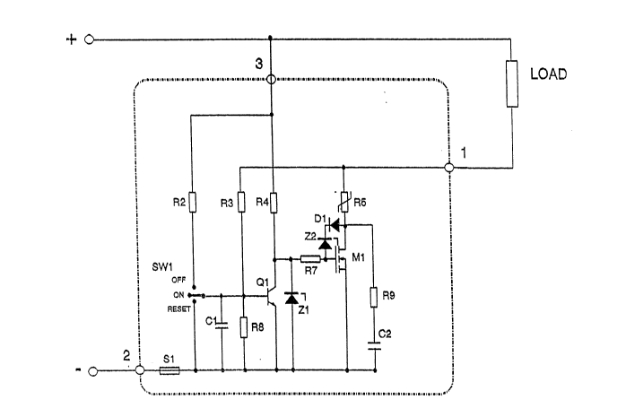
Figure l is a circuit diagram of a basic illustrative
embodiment of an inventive short-circuit
limiting device;
Figure 2 is a circuit diagram of a second embodiment
of an inventive short-circuit limlting de-
vice; ~ ;
Figure 3 is a circuit diagram of a third embodiment
of an inventive short-circuit limiting de-
vice;
Figure 4 is a circuit diagram of a fourth embodiment
of an inventive short-circuit limiting de-
vice; and
0 Figure S is a circuit diagram of a fifth embodiment
of an inventive short-circuit limiting de-
vice.
Descri~tion of Exem~lifvina Embodiments
Figure l is a circuit diagram which illustrates by way
of example a circuit which utilizes an electronic and
thermal feedback principle in accordance with the
present invention. ~he circuit diagram includes a
~ 94/11937 ~ PC~r/SE93/00956
number of resistors R2, R3, R4, R7, R8, R9 and a non-
linear temperature-dependent resistor R5. The circuit -
also includes a field effect transistor M1 in series
with the non-linear temperature-dependent resistor R5,
and a silicon diode D1 and two zener diodes Z1, Z2,
and a bipolar NPN-transistor Ql and two capacitors C1
and C2. According to the present invention, the main
functional part of the illustrated circuit is com-
prised generally of the components M1, R5, Q1, R4, R3
and R8. In the case of the illustrative embodiment,
the resistor R5 is a PTC-resistor of the type RUE 800
produced by Raychen Pontaisc SA, France. The field
effect transistor M1 is a power MOSFET, for instance
of the type MTW 45NlOE produced by Motorol~, and the
transistor Q1 is, for instance, a BC 847B transistor
produced by Motorola, for instance. Remaining resis-
tors, capacitors and di,odes are comprised of generally
available standard components. The zener rated voltage
of the zener diode Z1 is 12 volts, wh~le the zener
diode Z2 has a rated voltage of 90 volts.
The reference SW1 identifies a switch whlch has three
positions, OFF, ON and RESE~. When the switch is in
the OFF position, sufficient potential is applied via
the resistor R2 for the transistor Ql to conduct,
therewith blocking the field effect transistor Ml,
which consequently allows no current to pass through.
In other words, the load L is disconnected.
If the switch SW1 is briefly sw$tched to the RESET -
position, Q1 is activated and the voltage on the gate
of Ml will rapidly increase to the level determined by
the zener diode Zl and the voltage divider consisting
of resistors R4 and R7, where R4 is connected to the
positive terminal of the voltage source that supplies
the load L. The field effect transistor M1 will then
conduct current and the load L is thus activated. The
gate on Ml thus obtains a potential at which it is
fully conducting, wherewith the voltage drop across M1 -~
'-~94/11937 ~ PCT/SE93tO0956
in the case of moderate currents will be practically
negligible (one or some tenths of a volt). When the
switch SWl is then left in its neutral position, i.e.
its ON position, the circuit will opQrate in its
S operational mode. ~
The non-linear temperature-dependent resistor R5 is -
connec*ed in series with the thus created circuit, at
the collector connection of the transistor Ml. The
resistance of R5 is small at normal working tempera-
tures, in the same order of magnitude as the input or
ON-resistance of Ml. The two components Ml and R5 of
the preferred embodiment are mounted so that when
operating at normal current, thermal equilibrium is
obtained between the dissipated power generated and -
the heating power cooled-off from Ml and R5. These
components are mounted in good thermal contact with
the component carrying board (fiberglass board, ceram- -
ic substrate or a metal board, provided that the
components are insulated from the board). The non-
linear temperature-dependent resistor is also conve-
niently mounted so as to be also influenced by the
thermal energy developed by the tran~istor Ml. In the
case of an embodiment whlch includes discrete, encap-
sulated components, the transistor Ml is appropriately
provided with a cooling fin. The circuit created in
series with the load L and the positive and negative
terminal connection of the voltage source therewith
operates in its operational mode when the switch SWl
is in its ON position, so as to monitor the state of
the circuit in readiness to immediately break the
circuit of the load L at a predetermined overcurrent.
The following takes place when the current through the
load L exceeds the chosen overcurrent release value.
The temperature of both Ml and R5 will increase mark-
edly, wherein the increasing temperature of R5 will
cause the its resistance to increase rapidly, in an
accelerating fashion (non-linear dependency). The
094/11937 2 ~ 2 ~ PCT/SE93tO0956
~apidly increasing resistance in R5, and to some
extent also in Ml, together with the abnormal ~urrent
will result in an increasing voltage drop over R5 in
series with Ml. As a result of the action of a first
voltage divider consisting of the load L and the
combination of Ml and R5, the voltage across a second
voltage divider consisting of the resistors R3 and R8
supplying the transistor Ql increases. When the poten-
tial at the point between the resistors R3 and R8
which supply the base electrode on the transistor ~l
exceeds a given threshold value, Ql becomes conduc-
ting, whlch in a typical case occurs in a very short
time, in the order of microseconds, and therewith
short-circu ts the zener diode Sl and the transistor
Ml switches to a non-conducting state and the current
through the load L is broken.
After break~ng the current through the load L, the
whole of the supply voltage lies over the second
voltage divider consisting of resistors R3 and R8, and
Ql is consequently supplied with sufficient base
current to be fully conducting and therewith holds Ml
in a blocked, non-conducting state.
When a short-circuit occurs in the load L, the short-
circuiting current will increase rapidly and therewith
also the voltage drop over Ml and R5. A release or
turn-off sequence is initiated when the threshold
level of the base-emitter voltage for Ql is exceeded.
A desired time delay between the time of the non-
system current (the occurrence of the short-circuit)
and the release of Ml is obtained by suitable selec-
tion of the value of the capacitor Cl. The peak cur-
rent through Ml is determined by the value of the
capacitor Cl and by the inductance of the load L. If
Cl is excluded, the peak current is determined partly
by the base-emitter voltage for Ql and partly by the
quotient R3/R8. ~-;
~94/11937 ~ 2 ~ PCT/SE93/00956
If the trans~stor M1 is unable to break the short-
circuiting current, R5 will limit the maximum current
to a moderate value and then forces the current down
close to zero, by increasing its resistance very -
rapidly to several tens of thousands of ohms.
Sl is a typical, standard fuse which has a relatively
high value and justified by the requirements placed on
fuses by the authorities (the authorities do not
accept the use of solely an electronic circuit as a
short-circuiting protector), although the fuse Sl will
never be tripped or triggered in reality. -
When breaking an inductive load, the transient voltage
is limited by the zener diode S2 in coaction with the
field effect transistor Ml. The release time is deter-
mined by the zener voltage and the amount of inductive
energy that must be taken-up by Ml. The diode Dl
prevents current flowing through Z2 when Ml is fully
conducting. R9 and C2 are constructed to attenuate
oscillations when Ml is tripped ~so-called snubber
circuit).
Figure 2 illustrates another embodiment of the inven-
tion. In the Figure 2 embodiment, the circuit illus-
trated in Figure l has been supplemented with a fur- ~ -
ther bipolar transistor Q2, $or instance of the type
BC 847B with an associated th~rd voltage divider
consisting of the resistors RlO and Rll, a capacitor
C3 and a silicon diode D2.
The basic function of the circuit illustrated ~n
Figure 2 is the same as that of the circuit illustrat-
ed in Figure l, with the exception that the Figure 2 ~ ~;
circuit is reset automatically when a given period of ~ -
time has lapsed after release. The transistor Q2 is ~ -~
connected in parallel with the resistor R8, between
the base and emitter of the transistor Ql. The base
electrode on Q2 is supplied through the resistors RlO
9 ~ 12 7 q '11 pcr/sEs3/onss6
and Rll of the third voltage divider. When the tran-
sistor M1 breaks the current through the load L and
the voltage over the second voltage divider R3 and R8
is equal to the supply voltage, this voltage is also
obtained over the third voltage divider. Charging of
the capacitor C3 then com~ences via *he resistor R10,
to a voltage which corresponds to the dividing ratio
of R10 and Rll. When the voltage on the base electrode
exceeds the threshold voltage of Q2, after some period
of time, Q2 begins to conduct and the ~ransistor Q2
shunts-out the voltage level via the base electrode of
the transistor Q1, which therewith ceases to be con-
ducting. When the transistor Q1 becomes non-conduc-
ting, control voltage again appears on the gate of the
field effect transistor M1, which then again switches
to a fully conducting state and current can again flow
through the load L. When M1 again becomes conducting,
the voltage over the second and the third voltage
dividers disappears. ~he diode D2 then causes the
capacitor C3 to be guickly discharged, whereupon the
device as a whole is again in its operational mode.
If the fault (the short-circuit) remains, the device
again takes a bloc~ing state after a given time lapse,
the duration of which depends, among other things, on
the time constants of the combinations R9 and C2, and
R3, R8 and C1. The device will then break and make the
current at a given repetition frequency which will
depend on the time constants chosen in addition to the
aforesaid combination of R10, Rll and C3. ~ ;~
The circuit illustrated in Figure 2 includes two -
conventional light-emitting diodes D3 and D4 connected ;
in series with a respective current limiting resistor
R1 and R6. When supply voltage exists and the transis-
tor M1 is conducting, the diode D3 will shine to
indicate an ON-state. If the supply voltage remains
but no current flows through the load L and sufficient
voltage lies over the second (and third) voltage
~94/11937 ~ 7 l~ ~ ~ PCT/SE93/00956
divider, the ~iode D4 will shine (radiate) indicating
a triggering of the circuit. When the device i~ the
Figure 2 embodiment repeatedly breaks and makes the
current circuit, the diodes D3 and D4 will flash
alternately and therewith indicate this state. When
the repetition frequency is sufficiently high, the eye
of a viewer will experience the two diodes as radiat-
ing a marking which indicates a continued fault in the
load L.
Figure 3 illustrates a third embodiment of the present
invention, in which the circ1~it shown in Figure l is
supplemented with the diodes D3 and D4 and also an
optoswitch OPl, which in the case of the illustrative
embodiment is of the type CNY 74-4 produced by Tele-
funken. In this case, the light-emitting diode D3
shows when voltage is applied to the circuit and Ml is
conducting, while the light-emitting diode D4 shows -~
that the circuit is triggered. The optoswitch OPl lies
in series with D4, and at the same time as D4 receives
voltage and is ignited, the optoswitch OPl receives
the same current and is used to provide a remote ~;
indication that the circuit has been tripped.
::.
The circuit illustrated in Figure 4 is an extension of ;
the circuit illustrated in Figure 3, where the circuit
arrangement has been prepared for remote control with
the aid of two further optoswitches OP2 and OP3 of a
type corresponding to OPl. In this case, the emitter
electrode of a phototransistor in the optoswitch OP3
is connected by means of a further resistor Rl2 to the
collector electrode of a phototransistor in the opto-
switch OP2 and also to the base connection on the
transistor Ql. The current monitoring circuit can
therewith be remote controlled with the aid of the two
optoswitches, in addition to the direct control af-
forded by the switch SWl. When the optoswitch OP3
receives supply voltage, so that its incorporated
light-emitting diode will shine or radiate, the incor-
Q94/11937 ~ ~ 2 l ~ PCT/SE93/00956
porated phototransistor opens and current is led-in on
the base of the of the transistor Ql via the addition-
al resistor Rl2, and said base will then conduct
current which, in turn, switches the field effect - -
transistor to a non-conducting state, in accordance
with the aforegoing. Thus, the same function is ob-
tained as that when the switch Sl is switched to its
OFF position. This enables the load L to be switched
on and off by remote control.
Similarly, when the optoswitch OP2 receives a control
voltage, its phototransistor will short-circult the
base electrode of the transistor Ql to the negative
supply connection in a corresponding manner, which
corresponds to the function when the manual switch is
switched to the RESET position. In other words, the
circuit can be reset by remote control.
Finally, Figure 5 illustrates an exemplifying embodi~
ment in which the circuit according to Figure 3 is -
provided with an integrated circuit ICl instead of the -~
optoswitches OP2 and OP3. In the case of this embodi- -~
ment, the integrated circuit is comprised of a 5-volt ~-
logic circuit of the TTL type or the CMOS type, pref-
erably with an output level having three states. A
74LSl23 type IC-circuit is an example of a circuit
which can be used conveniently in the illustrative
embodiment. In this case, the output of the loglc
circuit is connected either to minus supply in the
case of the RESET function, and to positive supply in
the case of the OFF function, wherein the output will
normally take its floating state when the circuit is
in its ON function and therewith actively monitor the
current through the load L. The integrated circuit ICl
is controlled in accordance wlth prior art techniques
and enables the circuit to be readily applied in
digital applications.